Design and Modeling of Carbon Nanotube-Based Compliant Mechanisms
by
Christopher M. DiBiasio Sc.B., Mechanical Engineering (2005) Massachusetts Institute of Technology
Submitted to the Department of Mechanical Engineering in Partial Fulfillment of the Requirements for the Degree of
Master of Science in Mechanical Engineering at the
Massachusetts Institute of Technology February 2007
2007 Massachusetts Institute of Technology All rights reserved.
Signature of Author……… Department of Mechanical Engineering January 16, 2007
Certified by……… Martin L. Culpepper Rockwell International Associate Professor of Mechanical Engineering
Thesis Supervisor
Accepted by……...……… Lallit Anand Professor of Mechanical Engineering Graduate Officer
Design and Modeling of Carbon Nanotube-Based Compliant Mechanisms
by
Christopher M. DiBiasio
Submitted to the Department of Mechanical Engineering on January 16, 2007 in Partial Fulfillment of the Requirements for the Degree of Master of Science in
Mechanical Engineering
ABSTRACT
The objective of this research is to generate the knowledge required to adapt macro- and micro-scale compliant mechanism theory to design carbon nanotube-based nano-micro-scale compliant mechanisms. Molecular simulations of a nano-scale parallel guiding mechanism uncovered three regions of behavior. Region I is governed by the bulk deformation of the carbon nanotubes. Region II is characterized by hinge–like flexing of four “kinks” that occur due to buckling of the carbon nanotube walls. Region III, an intermediate region, exhibits direction dependant behavior. We report on the ability of a conventional compliant mechanism modeling approach, the pseudo–rigid–body model, to predict the region I behavior of a nano-scale parallel guiding mechanism that uses single–walled (5,5) carbon nanotubes as the flexural elements. Van der Waals forces were found to affect the kinematic and elastomechanic behavior of the nano-scale parallel guiding mechanism. A modified value of the pseudo–rigid–body model stiffness coefficient is presented to capture the affect of van der Waals interactions within (5,5) nanotubes during region I operation. Molecular simulation of region I behaviors match the modified pseudo–rigid–body model predictions of (1) kinematic behavior with less than 7.3 % error and (2) elastomechanic behavior with less than 8 % error. Although region I is of the most interest because of its well-defined and stable nature, region II motion is also investigated to provide a basis for establishing future work in this region.
Thesis Supervisor: Martin L. Culpepper
ACKNOWLEDGEMENTS
I would like to thank my thesis advisor Martin Culpepper for the guidance he provided me as I conducted the research that would eventually lead to this thesis. He has provided me with advice that has not only made me more adept at research and engineering, but has also helped me to develop professionally. I look forward to continue working with him and learning from him as I pursue my doctorate.
I would also like to thank my colleagues in the Precision Compliant Systems Laboratory. Their advice on conducting research and the stresses of graduate life has helped me maintain balance in my life as a graduate student. I would especially like to thank Amos Winter and Robert Panas for their contributions in creating the initial models used in the simulations that were included in this thesis.
I also need to thank my family and friends for all of their support over the last year and a half. Without the emotional support they have given me, I do not know if it would have been possible to have completed this work. I also need to thank my mother and father who, after supporting me through my undergraduate program, continue to provide me financial and emotional support. The successes I have achieved in my life I owe in large part to them.
Finally, I must thank those who financially supported my graduate research. I would first like to thank former MIT President Charles Vest and his wife Rebecca for providing me with a fellowship during my first year in graduate school. Having a fellowship enabled me to define a research path that I was genuinely interested in, not just a project that was financially supported. Lastly, I would like to thank Rockwell International and the Karl Chang Innovation Fund at MIT for supporting the last six months of my research.
Table of Contents
Abstract ... 3 Acknowledgements... 5 Table of Contents... 7 List of Figures ... 9 List of Tables ... 11 Chapter 1... 13 1.1 Importance ... 141.1.1 Need for Nano-scale Devices... 14
1.1.2 Role of Compliant Mechanisms in Nano-electro-mechanical Systems... 17
1.1.3 Fabrication Challenges at the Nanometer Level... 20
1.1.4 Performance Limitations Due to Material Properties ... 21
1.1.5 Carbon Nanotubes as a Nano-scale Flexure Material... 21
1.2 Overview of Prior Art ... 22
1.2.1 Small-Deformation Devices... 22
1.2.2 Large-Deformation Devices... 24
1.2.3 Relative Rotation/Sliding Devices... 26
1.2.4 Relevance of Prior Art to Carbon Nanotube-based Flexures... 27
1.3 Scope... 28
1.3.1 Fundamental Issues... 28
1.3.2 Parallel Guiding Mechanism Case Study ... 29
1.3.3 Thesis Outline ... 30
Chapter 2... 31
2.1 Structure of Carbon Nanotubes... 31
2.2 Physical Properties of Carbon Nanotubes... 36
2.2.1 Continuum Definitions of Mechanical Properties at the Nano-scale... 37
2.2.2 Properties of Axial Deformation... 37
2.2.3 Properties of Bending Deformation ... 40
2.2.5 Affect of Chirality on Mechanical Properties... 44
Chapter 3... 47
3.1 Molecular Simulation... 47
3.1.1 Ab Initio Simulation... 48
3.1.2 Space Frame Simulation ... 49
3.1.3 Finite Element Simulation ... 50
3.1.4 Molecular Mechanics and Dynamics Simulations... 51
3.2 Psuedo-rigid-body Model for Compliant Mechanisms... 54
Chapter 4... 61
4.1 Molecular Model Used in the Simulations ... 61
4.2 Simulation Results ... 66
4.2.1 Simulated Kinematics ... 66
4.2.2 Simulated Elastomechanics ... 70
4.2.3 Role of van der Waals Forces on Nano-scale Compliant Behavior... 74
4.2.4 Geometric Nonlinearity as a Cause for Direction-dependant Behavior ... 78
4.2.5 Energy-displacement Relationship ... 78
Chapter 5... 83
5.1 Psuedo-rigid-body Model Parameters... 83
5.2 Psuedo-rigid-body Model Predicted Kinematics ... 84
5.3 Psuedo-rigid-body Model Predicted Elastomechanics ... 85
5.4 Improving the Psuedo-rigid-body Model Predictions... 86
5.4.1 Optimizing the Characteristic Radius Factor... 87
5.4.2 Optimizing the Stiffness Coefficient ... 88
Chapter 6... 91
6.1 Summary... 91
6.2 Future Work ... 93
References... 97
Appendix A: nPGM Kinematic Data... 101
Appendix B: nPGM Elastomechanic Data ... 105
Appendix C: nPGM Strain Energy Data... 107
List of Figures
Figure 1.1: Schematic of AFM operation (a) and a close-up of an AFM tip on substrate (b)... 16
Figure 1.2: A compliant parallel-guiding mechanism. ... 18
Figure 1.3: A micro-scale six-axis compliant positioning stage by Chen and Culpepper... 19
Figure 1.4: Close-up of CNT-based nanotweezers (a) and nanotweezers in operation (b). ... 22
Figure 1.5: Schematic of a CNT-based relay (a) and CNT-based memory (b). ... 23
Figure 1.6: Schematic of a CNT-based transistor (a) and its physical realization (b). ... 24
Figure 1.7: Schematic of the rotational CNT bearing (a), an SEM photo of the realized device (b), and a close-up of the CNT anchor (c). ... 25
Figure 1.8: Theoretical operation of an axially bistable CNT switch... 25
Figure 1.9: Schematic of a CNT-based motor (a) and pictures of the rotor in motion (b). ... 26
Figure 1.10: Schematic of a CNT axial bearing (a) and pictures of the realized device (b)... 27
Figure 1.11: A one degree-of-freedom linear motion stage... 30
Figure 2.1: Graphene sheet to CNT analogy. ... 32
Figure 2.2: Chiral vector definition on a graphene sheet... 33
Figure 2.3: Zig-zag (a) and armchair (b) carbon nanotube chiralities. ... 34
Figure 2.4: Stone-Wales defect in a SWCNT ... 35
Figure 2.5: Activation energy for a Stone-Wales defect in a SWCNT... 36
Figure 2.6: Localized buckling during SWCNT bending... 42
Figure 2.7: MWCNT wave-like distortion during bending. ... 43
Figure 3.1: Four-bar flexure and its PRBM representation. ... 55
Figure 3.2: Placement of pivots according to characteristic radius factor... 56
Figure 3.3: Geometry parameters that define the PRBM representation of a PGM. ... 57
Figure 4.1: MM/MD model of CNT-based nPGM... 62
Figure 4.2: Constraints placed on the SWCNT cross-section... 62
Figure 4.3: Constraints placed on the SWCNT to form the coupler bar... 63
Figure 4.4: Coupler bar centroid translation. ... 67
Figure 4.6: Coupler bar centroid translation. ... 68
Figure 4.7: Parasitic rotation of the coupler bar. ... 70
Figure 4.8: Force-displacement response of the coupler bar. ... 71
Figure 4.9: Loading/unloading response of the coupler bar in the transition region... 72
Figure 4.10: Force/displacement of the coupler bar with van der Waals interactions turned off. 74 Figure 4.11: Van der Waals interactions in the non-bonded SWCNT cross-section... 75
Figure 4.12: Van der Waals force as a function of atomic separation, r. ... 75
Figure 4.13: Cross-section deformation during simulation (a), and van der Waals interactions for the kinked structure (b). ... 76
Figure 4.14: Longitudinal cross-sections of the first kink for points of interest... 77
Figure 4.15: Strain energy in the nPGM as a function of horizontal centroid motion. ... 79
Figure 4.16: MM and MD force-displacement data for the nPGM. ... 80
Figure 5.1: PRBM versus MM kinematics for the nPGM... 85
Figure 5.2: PRBM versus MM elastomechanics for the nPGM. ... 86
Figure 5.3: Affect of γ on PRBM predicted region I elastomechanics. ... 87
Figure 5.4: Affect of γ on PRBM predicted region I kinematics. ... 88
List of Tables
Table 1.1: Bulk mechanical properties of silicon. ... 21
Table 2.1: Elastic properties of CNTs in axial extension. ... 38
Table 2.2: Failure properties of CNTs in axial extension... 39
Table 2.3: Elastic properties of CNTs in axial compression. ... 39
Table 2.4: Failure properties of CNTs in axial compression... 40
Table 2.5: Elastic properties of SWCNTs in bending... 41
Table 2.6: Elastic properties of SWCNTs in torsion. ... 44
Table 3.1: Elastic properties of the space frame. ... 49
Table 4.1: Parameters that define the nPGM model... 64
Table 4.2: Coupler bar locations at points of interest during loading/unloading of the nPGM.... 69
Table 4.3: Net cross-sectional force for kink 1 at during loading/unloading of the nPGM. ... 77
Table 5.1: Criterion for modeling SWCNT as a hollow cylinder... 84
Table 5.2: Initial PRBM parameters for the nPGM... 84
Table A1: Coordinates of the coupler bar centroid during MM simulation. ... 101
Table A2: Rotation of the coupler bar centroid during MM simulation... 102
Table B1: Horizontal load and displacement of the coupler bar during MM simulation... 105
Table B2: Force/displacement data for the no van der Waals interaction MM simulations... 106
Table C1: Strain energy and displacement of the nPGM during MM simulation... 107
Chapter 1
Introduction
The objective of this research is to generate the knowledge required to adapt macro- and micro-scale compliant mechanism theory to design carbon nanotube-based nano-scale compliant mechanisms. Compliant mechanisms are systems of rigid and flexible elements that use the bending deformation of the compliant members to guide smooth and continuous motion of rigid components [1]. Carbon nanotube-based nano-scale compliant mechanisms are important because they may provide the means to produce nano-scale devices while avoiding (1) the size limitations imposed by current nano-fabrication techniques and (2) the mechanical property limitations that are possessed by nano-scale materials. The realization of carbon nanotube-based compliant mechanisms would allow scientists and engineers to design smaller (100 times smaller than current micro-scale devices) and faster (over 1000 times faster than current micro-scale devices) compliant mechanisms for devices. The design and fabrication of compliant mechanisms at the macro- and micro-scale have been practiced for decades, however, the incorporation of the most rudimentary flexures within nano-scale mechanical systems is a recent development [2]. There are two major roadblocks to using macro- and micro-scale compliant mechanism research at the nano-scale: 1) material limitations and 2) fabrication limitations. Conventional nano-scale fabrication methods are compatible with a limited set of materials. The mechanical properties of these materials impose a limit on the elastic deflections of nano-scale flexures that is approximately 20% of the flexure’s characteristic length. Conventional nano-fabrication process capabilities limit the size and accuracy of features on the order of a few tens of nanometers, and this level of uncertainty would mean that a match between model and measured performance could only be obtained using parts measuring hundreds of nanometers. In light of these limitations a new approach for engineering nano-scale flexure-based devices will be needed.
Carbon nanotubes are single molecules that possess high strength (failure stress ~100 GPa [3]) and large failure strains (~40% [4]) in comparison to conventional engineering materials. These properties make them attractive for use in nano-scale compliant mechanisms. The majority of current research has focused on characterizing, understanding, and modeling the physical properties of carbon nanotubes. Little work has been done understand how to incorporate carbon nanotubes into simple nano-scale mechanical elements that are deterministically engineered to meet a set of design specifications. As a result, no one has determined if/how conventional compliant mechanism theory may be adapted so that carbon nanotube-based nano-scale compliant mechanisms may engineered. These devices could be driven at speeds 1000 times faster than their micro-scale counterparts. This is because the natural frequency of a device scales with the inverse of the square-root of its mass. It is clear that the behavior of a carbon nanotube-based compliant mechanism will need to be investigated and subsequently modeled before design synthesis and fabrication research becomes feasible.
1.1 Importance
Over the last twenty years, research has been conducted to move macro-scale devices and technologies to the micro-scale. Micro-electro-mechanical systems (MEMS) are now used in consumer products ranging from automobiles (airbag accelerometers) to cellular phones (microphones), and even home theater systems (micro-mirrors in digital light processing (DLP®) televisions). For scientists and engineers, the introduction of MEMS technology into fields such as communications (fiber optics positioning) has allowed for the development of state-of-the-art systems that perform tasks that were impractical or impossible at the macro-scale. As engineers have started to master the art of MEMS design and fabrication, their focus has shifted towards the next level: nanometer-level devices.
1.1.1 Need for Nano-scale Devices
While the benefits of making electronic components smaller is clear (less power consumption and higher computation density), the role of nano-electro-mechanical systems (NEMS) is not well-defined. In order to understand the need for NEMS it is important to look at the benefits of miniaturizing a mechanical system:
1. High Speed: The natural frequency of a device scales with the
inverse of the square root of the system mass. This smaller mass, therefore, leads to less inertial forces which corresponds to higher system natural frequencies. This allows the device to be driven at faster device driving frequencies. For instance, a 10x10x10 nm3 mass may be driven 1000 times faster than a 1 µm3 mass of the same material, assuming each mass is attached to a spring of similar stiffness.
2. Scale Matching: It is difficult to manipulate objects on the
nano-scale using MEMS devices as the system scales are mismatched, typically over three orders of magnitude difference. When system components are the same order of magnitude in size as the item to be manipulated, it is in general easier to accomplish those tasks. When scale mismatches occur in a system a de-amplification or amplification mechanism must be introduced. In order to attenuate a displacement input a compliant member must be introduced in the load path. Since the system natural frequency scales with the square root of the load path stiffness, adding a compliant spring in series with the applied load has an adverse affect on the system stiffness.
3. Smaller Footprint: A smaller device footprint leads to device
integration in systems where space and/or weight is a premium. This smaller size will drive innovation in many different areas such as sensors, actuators, and manipulators.
While the preceding list is not all-inclusive, it is important to keep these benefits in mind when evaluating the need for NEMS devices. The remainder of this section will discuss each of the preceding benefits in more detail.
The enhancement of system speed is perhaps the most important benefit of operating at the nano-scale. Many nano-scale probing and imaging technologies are fundamentally limited in their operational speed due to the natural frequencies of their components. A good candidate for
the introduction of a NEMS based module would be, for instance, an atomic force microscope (AFM). Figure 1.1 depicts the basic operating principles of an AFM in the “tapping” mode.
(a) (b)
Figure 1.1: Schematic of AFM operation (a) and a close-up of an AFM tip on substrate (b). During operation, a laser beam aimed at the back of a silicon cantilever reflects onto a quadrant photo-detector, and the deflection of the laser on the photo-detector allows for measurement of the surface height. By raster scanning the surface in a pixel-by-pixel fashion, a surface profile may be generated for the sample, as shown in Fig 1.1(b). CNT-based mechanisms could replace micro-scale cantilevers and enable increased speeds that could for instance make video rate AFM's possible.
Another advantage of nano-scale devices is that they minimize the scale mismatch problem inherent when using macro- and micro-scale devices to perform nano-scale tasks. De-amplification is necessary for most micro- or macro-scale actuators because their displacement and force outputs are at least three orders of magnitude larger than the intended nano-scale output. The most common method of attenuating force and displacement outputs from an actuator is to use a flexure, as will be discussed in section 1.1.2. In order to attenuate an actuator displacement input, the flexure must be extremely compliant. This means the effective spring constant for the compliant member is small. This de-amplification may achieve the static needs of the system, but the system dynamics are adversely impacted as a result. Since system natural frequency scales with the square root of the system’s effective spring constant, adding a
compliant flexure lowers the overall system natural frequency. This increases the system’s sensitivity to low frequency vibrations that are commonly present in the environment surrounding the system. These low frequency vibrations may easily introduce nanometers to microns worth of displacement into the system, which could greatly reduce the performance of the system. These inherent problems of scale mismatch could be averted by using nano-scale devices to perform nano-scale tasks.
Nano-scale devices could have a large impact in the fields of biology, chemistry, physics, and nano-fluidics. A nano-scale device capable of grasping individual molecules could allow mechanical manipulation of proteins, giving biologists and chemists new tools for studying and synthesizing proteins [5]. The ability to grasp individual DNA strands and “cut” them would allow for advanced faster genomic sequencing, which could lead to greater advances in genetic testing and therapy [5, 6]. Also, a nano-scale device could be used to probe individual organelles in cells, allowing biologists to be able to more quickly understand and model cell function as well as create new cell therapies [7]. Using a nano-scale manipulator, physicists would also be able to manipulate quantum dots more easily and effectively, allowing for rapid advances in fields such as quantum computing [8]. Engineers working in the field of nano-fluidics have promised compact biological and chemical sensors, “lab-on-a-chip” products, and even artificial cells and organelles [9]. In order to build these fluidic systems, however, there needs to be a nano-scale equivalent of a fluid pump and a binary on/off valve [10].
It is also important to realize the impact of the small nano-scale device footprint on information density. NEMS based transistors, relays, and nonvolatile memories have the ability to contribute to the electronics industry [11]. They would allow smaller chips that consume less power and have more computational capacity to be produced, which would greatly impact the role of computing in everyday life. Communications would also see an impact from nano-scale devices by way of denser fiber optic interconnects. Nano-scale devices could serve as optic alignment stages as well as mirror positioning stages.
1.1.2 Role of Compliant Mechanisms in Nano-electro-mechanical Systems
It is important to examine how MEMS devices are constructed when discussing how a NEMS device might be embodied. Most MEMS devices consist of 1) an actuator, 2) bearings, 3) moving member, 4) a support structure, and 5) a metrology system. Research has been
conducted on the design and fabrication of actuators and metrology systems for nano-scale applications, but little work has been done on miniaturizing the necessary bearings and support structure. This is unfortunate, as the preferred embodiment of bearings at the MEMS level are flexures, and little is known about how they will be embodied or how they will perform at the nanometer level.
Compliant mechanisms (CM) are mechanical devices in which one or more components are deformed elastically in order to guide motion. Figure 1.2 shows a compliant parallel-guiding mechanism, which consists of a rigid coupler and grounding bar as well as two compliant members, in an undeformed (shaded) and deformed state.
Figure 1.2: A compliant parallel-guiding mechanism.
The advantages of using a CM as the support structure and bearing for the coupler bar are that CMs 1) do not require assembly, 2) experience little subject to hysteresis due to friction during operation, 3) are subject to little energy dissipation during operation, 4) are inherently deterministic in nature, and 5) may be cycled many times without performance loss provided the loading level produces stresses less than the critical failure stress of the material.
As will be discussed in section 1.1.3, most nanofabrication processes are 2½ dimensional processes. As a result, most MEMS devices consist of planar features whose thickness is defined by the silicon device layer thickness. Figure 1.3 shows a picture of a six axis positioning stage by Chen and Culpepper [12].
Figure 1.3: A micro-scale six-axis compliant positioning stage by Chen and Culpepper1. It consists of a central positioning stage connected to flexure beams which are further connected to thermal actuators. The manipulator has a 10 µm maximum range. The topology formed by the CM based device conforms to the requirements of 2½ dimensional fabrication, as the entire device consists of a planar geometry. Using CMs in MEMS devices eliminates the need for micro-scale assembly, which is difficult due to the scales of the parts involved in the assembly. As part sizes become sub-micron in size, forces due to surface tension and electrostatic interaction make small part alignment and manipulation nearly impossible. Using a standard scaling law for CMs, the ratio of elastic modulus to yield strength of the material [3,13], a carbon nanotube based six-axis positioner would have almost three times the range of the positioner made by Chen and Culpepper [12].
Perhaps the most important benefit in using CMs for bearings and the support structure in MEMS devices is the deterministic nature of the flexural components. Deterministic devices have a single output for any input, and furthermore, these outputs are usually easily mapped. As flexures do not experience significant friction, stiction, or slip during their operation, three problems inherent in motion guidance components held together by pin joints or bolts, this removes a source of hysteresis from the system. Furthermore, the primary mode of energy storage during the deflection of the flexure is through the stretching of atomic bonds. As such, there is little energy loss while cycling a flexure blade under load. A CMs deterministic nature is not affected by manufacturing error as an improperly manufactured flexure will still give one
output for a single input. The change in stiffness resulting from manufacturing error will require that the CM be calibrated.
1.1.3 Fabrication Challenges at the Nanometer Level
Ideally one would like to take the knowledge gained from MEMS research and apply design and fabrication rules to a NEMS device. Unfortunately the predominant method of MEMS fabrication, projection lithography [14], is not an option in the fabrication of a nano-scale device. The diffraction limit of lithography sets the resolution for fabricated geometries. Equation 1.1 shows the relationship of minimum feature size, wmin, to the radiation wavelength,
λ, and numerical aperture, NA [14].
= NA wmin 2 2 1 λ (1.1) Currently the state-of-the-art in projection lithography is an ArF laser with a wavelength of 193 nm and a lens system utilizing immersion lithography with a numerical aperture of 0.9. Accordingly, the minimum feature size under ideal conditions is approximately 50 nm, a far cry from the nanometers of resolution desired for nano-scale CMs. The next semiconductor industry target for projection lithography is the 32 nm node, and it is unknown at this time whether or not projection lithography will meet the resolution demands for this next node. Development of radiation sources with finer wavelengths is ongoing, but progress has been slow. Advances in immersion lithography have made slight improvements in system numerical aperture, but not enough to produces a useful impact on minimum feature resolution. If nano-scale devices are to be built with flexural components, an alternative fabrication method is needed.
Electron-beam lithography (EBL) [14] could prove to be a viable alternative fabrication method for nano-scale features. The advantage of EBL is that device features of 5-10 nm are possible. However, because of the pixel-by-pixel nature of the process, writing times for an exposure are slow. To expose 50% of 4 nm2 pixels requiring 100 electrons of exposure in a 1 cm2 area, even the best EBL machines would take approximately three days to complete the pattern. If nano-scale devices are to be produced massively in parallel, another fabrication technique will need to be utilized.
Nano-imprint lithography (also referred to as soft lithography) [15] is another alternative for fabrication at the nano-scale. Hua et al have shown that polymer molds replicating carbon nanotubes with diameters on the order of a few nanometers can create features in silicon with
nanometer resolution [16]. Unfortunately, soft lithography is mainly used as a method of replicating an existing feature. This makes it impractical for fabrication of nano-scale compliant mechanisms.
1.1.4 Performance Limitations Due to Material Properties
Even if a fabrication method existed that could create nanometer features, there are performance limitations that stem from the physical properties of the principal material used in MEMS devices, bulk silicon. The most relevant bulk mechanical properties for CM design are presented in Table 1.1 for single crystal silicon [13]. For a silicon cantilever beam 10 µm thick, 50 µm wide, and 100 µm long, failure in the beam would occur at 3.68 µm axial extension or 24.5 µm lateral tip deflection. Since silicon is a brittle material and does not plastically deform, it is common practice to introduce a safety factor in practical device designs in order to avoid possible beam fracture. This safety factor decreases the total elastic beam bending deflection in the flexure.
Table 1.1: Bulk mechanical properties of silicon.
Elastic Modulus 190 GPa
Failure Strength 7 GPa
Density 2300 kg/m3
1.1.5 Carbon Nanotubes as a Nano-scale Flexure Material
Carbon nanotubes (CNTs) were first discovered by Iijima in 1991 [3]. They are single molecules of carbon that take the form of tubes with diameters on the order of nanometers. Due to their exceptional mechanical properties, CNTs show promise to be a useful material to incorporate into NEMS devices . It has been shown that CNTs may undergo elastic strain in excess of 40% [4], which is larger than any materials currently used in MEMS devices. Furthermore, CNTs are grown from catalyst particles whose size roughly dictates the diameter of the CNT, which means that fine feature sizes may be attained without the use of lithography. If CNTs could be incorporated as the flexural components of nano-scale compliant mechanisms (nCMs), it may be possible to realize nano-scale devices with greater range and smaller feature sizes than their silicon counterparts.
1.2 Overview of Prior Art
The majority of research has been conducted via simulation, and the majority of physical prototypes that have been produced are one degree-of-freedom mechanisms with simple topologies and functions. Almost all of the realized devices operate in the CNT small-deformation regime while the majority of the simulation work has been carried out on the more complicated large-deformation devices and designs that exploit the relative sliding and rotation of multi-walled CNTs.
1.2.1 Small-Deformation Devices
The first class of CNT-based mechanisms rely on the stretching of atomic bonds in torsion as well as bending to produce small one degree-of-freedom motion, i.e. deflections less than 10% of the flexure’s characteristic length. In one of the first demonstrations of using CNTs as a compliant mechanical element, nano-scale tweezers have been demonstrated as an effective means of grasping and manipulating nano-scale particles [17-19]. Figure 1.4(a) shows the profile of the tweezers, which consist of a split electrode with CNT bundles attached at the tip.
(a) (b)
Figure 1.4: Close-up of CNT-based nanotweezers2 (a) and nanotweezers in operation3 (b). When a voltage difference is applied at the split electrode, the electrostatic force produced by the ~10 V potential difference forces the CNT bundles, isolated on different electrodes, to bend towards each other. This small-scale deformation allows for the grasping (as shown in Fig. 1.4(b)), manipulation, and release of particles of 100 nm or less.
2 Figure 1.4(a) reproduced with permission from P. Kim and C. Lieber. Science 286 (5447), 2149 (1999). Copyright
2007 by the American Association for the Advancement of Science.
3 Figure 1.4(b) reproduced with permission from S. Akita and Y. Nakayama. Jap. J. App. Phys. 41 (6b), 4242
Electrostatic attraction has also been proposed as a method for actuating CNT-based mechanical relays [20], non-volatile memory [21], and transistors [22] at the nanoscale. The relay in Fig. 1.5(a) uses a voltage differential applied by the gate electrode (G) to deflect the CNT into contact with the drain electrode (D), thus completing an electrical circuit with the source (S) and drain electrodes. Mechanical tests showed a 9 nN load deflected the 1.8 µm long CNT 80 nm laterally. The device had a resonance frequency of 0.1 GHz, though the authors claim that smaller nanotubes could be used in future applications to allow for higher natural frequencies.
(a) (b)
Figure 1.5: Schematic of a CNT-based relay4 (a) and CNT-based memory5 (b).
Figure 1.5(b) shows a schematic of non-volatile CNT-based memory. The memory consists of a grid of CNTs that are perpendicular to one another. Electrodes at the end of each CNT allow for the application of a differential potetial. By applying these voltage differences to different CNT pairs, the overlayed CNTs may be brought into contact with those that are laying under it. Once in contact, van der Waals attractive forces hold the two CNTs in contact even without the presence of the potential difference, forming a non-volatile “ON” state. Simulation results indicate that this device could be operated at speeds greater than 100 GHz. The CNT-based transistor shown in Fig. 1.6(a) uses uses the lateral bending of three vertical MWCNTs to create electrical contacts. The outermost CNTs have opposite potentials applied to them. When the
4 Figure 1.5(a) reproduced with permission from S.W. Lee, D.S. Lee, R.E. Morjan, S.H. Jhang, M. Sveningsson,
O.A. Nerushev, Y.W. Park, and E.E.B. Campbell. Nano Lett. 4 (10), 2027 (2004). Copyright 2007 by the American Chemical Society.
5 Figure 1.5(b) reproduced with permission from T. Rueckes, K. Kim, E. Joselevich, G.Y. Tseng, C. Cheung, and
C.M. Lieber. Science 289 (5476), 94 (2000). Copyright 2007 by the American Association for the Advancement of Science.
central CNT has a potential applied to it, it feels an attractive electrostatic force to one of the outer CNTs. The outer CNT that the central CNT contacts depends on the sign of the potential applied to the central CNT. The attractive force caused by the 22.4 V potential difference induced deformation leading contact between the central and outer CNTs (1.4 µm in length), thereby making an electrical connection, as shown in Fig. 1.6(b).
(a) (b)
Figure 1.6: Schematic of a CNT-based transistor (a) and its physical realization6 (b).
1.2.2 Large-Deformation Devices
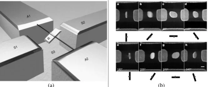
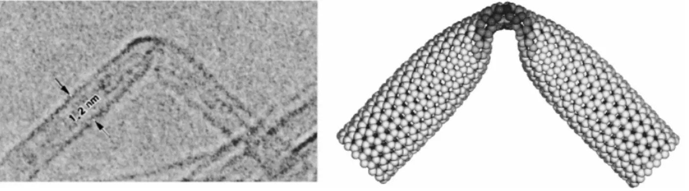
The second class of CNT-based devices are capable of deflections that are greater than 10% of their characteristic length and/or exhibit buckling phenomenon during operation. In one of the first demonstrations of a large motion CNT bearing, the torsional deflection of a CNT has been used to form a large rotation bearing [23-24] for a nano-scale pendulum. As shown in Fig. 1.7(a), the pendulum is suspended from a CNT which lays across two anchor pads, as seen in Fig. 1.7(b). The bond between the CNT and an anchor is detailed in Fig. 1.7(c). The authors in [23] report that the pendulum is supported by a total of forty carbon-carbon (C-C) bonds via the 1.5 nm diameter CNT. Using an external electric field for actuation, the pendulum is capable of 180o of reversible rotation. The CNT bearing possess a spring constant of 2.86 nN⋅nm/rad and a resonance frequency of 0.1 MHz.
6 Figure 1.6 reproduced with permission from J. E. Jang, S. N. Cha, Y. Choi, Gehan A. J. Amaratunga, D. J. Kang,
D. G. Hasko, J. E. Jung, and J. M. Kim, Appl. Phys. Lett. 87, 163114 (2005). Copyright 2007 by the American Institute of Physics.
(a) (b) (c)
Figure 1.7: Schematic of the rotational CNT bearing (a), an SEM photo of the realized device (b), and a close-up of the CNT anchor7 (c).
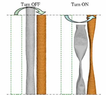
It has been shown that a CNT may buckle if subjected to an axially compressive load. Since a buckled CNT undergoes a change in electrical properties it has been proposed [25] to use this phenomenon to produce a switch at the nano-scale. The authors have simulated the performance of this device and found that a 1% compressive strain will cause the device to buckle as shown in Fig. 1.8 and reside in the “ON” state. At 1.29% tensile strain the CNT was found to revert to its undeformed state. The authors have found that this buckling event is a bistable event for certain diameters of CNTs.
Figure 1.8: Theoretical operation of an axially bistable CNT switch8.
7 Figure 1.7 reproduced with permission from J.C. Meyer, M. Paillet, and S. Roth. Science 309 (5740), 1539 (2005).
Copyright 2007 by the American Association for the Advancement of Science.
8 Figure 1.8 reproduced with permission from T. Chang, J. Hou, and X. Guo, Appl. Phys. Lett. 88, 211906 (2006).
1.2.3 Relative Rotation/Sliding Devices
The third class of CNT-based mechanisms exploit the nested tube structure of multi-walled CNTs in order to make rotary and sliding bearings at the nano-scale. Rotary bearings [26-28] seem to be of most interest, as a technique has been developed for trimming the outer shell of a multi-walled CNT in order to free it from its anchor, allowing relative motion between the inner and outer shells of the CNT. The idea of a CNT-based motor, as shown in Fig. 1.9(a), may be realized [28] by actuating a rotor that rests on the outer shell of a multi-walled nanotube (~ 50 nm in diameter). When the rotor is actuated by the stator, the rotor causes the walls of the CNT to rotate relative to each other, forming a low-friction sliding contact bearing that allows the rotor a full 360 degree rotation, as shown in Fig 1.9(b).
(a) (b)
Figure 1.9: Schematic of a CNT-based motor (a) and pictures of the rotor in motion (b)9. Research has also been conducted on using multi-walled CNTs to produce axial sliding bearings [29]. Figure 1.10(a) shows the axial sliding bearing concept. A multi-walled “bamboo” type CNT is anchored to a substrate at one end, while the other end is partially cleaved off, exposing an inner bundle of walls. The inner core of the CNT is then brought into contact with the target object, which sticks to the inner core via van der Waals forces. This target object is now supported by the bearing formed by the inner core sliding within the outer shell of the multi-walled CNT, as shown in Fig. 1.10(b).
9 Figure 1.9 reproduced by permission from Macmillian Publishers Ltd: W. Han, A.M. Fennimore, T.D. Yuzvinksly,
M.S. Fuhrer, J. Cumings, and A. Zettl. Nature 424 (6947), 408 (2003). Copyright 2007 by Macmillion Publishers Ltd.
(a) (b)
Figure 1.10: Schematic of a CNT axial bearing (a) and pictures of the realized device (b)10. The major research to date for relative rotation/sliding devices has focused on (1) determining the energy required to initiate and maintain relative motion between walls of the CNT and to (2) model the energy that is dissipated within these devices. The simulated [29,30] and measured [31] “friction” surface stresses appear to be low enough (0.85 MPa) so that “wear”, i.e. removal of the carbon atoms from the CNT structure, appears unlikely at room temperature.
1.2.4 Relevance of Prior Art to Carbon Nanotube-based Flexures
While the prior art has succeeded in creating a functional torsional bearing, a functional linear bearing has not been realized. Furthermore, the prior art has not yet been able to utilize multiple CNTs to create a true compliant system. The lack of simulated and fabricated large deformation compliant mechanisms with CNT-based flexural components means that nano-scale devices cannot be constructed using knowledge learned from macro- and micro-scale device research.
10 Figure 1.10 reproduced by permission from J. Cumings, and A. Zettl, Science 289 (5479), 602 (2000).. Copyright
1.3 Scope
There is a need to investigate the behavior of, and subsequently model the performance of, CNT-based flexures before a CNT-based nCM may be realized. While the benefits of, and need for, nCMs have been established, the knowledge generated from current research on devices with CNT-based components is inadequate for understanding and predicting the behavior of CNT-based flexures. CNT-based CMs are fundamentally different than macro-scale CMs because they are subject to nano-scale phenomenon such as van der Waals interactions and possess fundamentally different material properties.
1.3.1 Fundamental Issues
In, the following needs to be understood in order for CNTs to be usable as a flexural element in a nCM:
1. The kinematics of a CNT-based flexural element.
2. The relationship between the applied force and deformation of
the CNT-based flexural element, i.e. the elastomechanics.
3. The actuation requirements, force and stroke, must be
compatible with NEMS actuators.
4. If macro-scale CM design theory may be adapted and then
applied to a CNT-based nCM.
5. If macro-scale CM design theory is unable to describe the
behavior of CNT-based nCMs, is it possible to adapt it in order to capture nano-scale behaviors?
If satisfactory answers to all five questions may be found, then one may proceed in the design and fabrication of a CNT-based nCM.
While preliminary testing of CNTs via tensile testing and nano-indentation shows promise for their use as flexural members, this is not definitive proof. One needs to focus on the kinematic and elastomechanic behavior of a CNT-based flexural element In order to determine whether or not CNTs are good candidates for acting as the flexural members of a nCM. The kinematic and elastomechanic behavior of a nCM must be compared with that of a macro-scale CM. Since nano-scale forces such as van der Waals interactions become more dominant than many macro-scale body forces phenomena such as gravity at the level of CNTs, it is possible for
nCMs to act differently than macro-scale CMs. Furthermore, the range and loading characteristics must be looked at versus current state of the art nano-scale actuators to determine if a CNT-based nCM will be compatible with current actuation technologies.
If CNTs appear to be reasonable candidates for incorporation into nCMs, it will become necessary to predict their performance before device fabrication occurs. It is well known that the continuum descriptions of a material breaks down at ~10 nm, forcing one to make modifications to many basic engineering equations at this level. Since many precision engineers who design CMs are well-versed in analysis methods such as the psuedo-rigid-body model, it seems natural to adapt macro-scale CM design tools to suit the needs of describing nano-scale flexural elements. The fundamental differences in CNT mechanical behavior and macro-scale material behavior prevents us from knowing a priori if the pseudo-rigid-body model is capable of analyzing CNT-based nCMs.
1.3.2 Parallel Guiding Mechanism Case Study
In order to answer the above questions a ubiquitous element of macro- and micro-scale CMs, a four-bar parallel guiding mechanism (PGM), will serve as a case study. PGMs are one degree-of-freedom CMs that consist of two flexural members and two rigid members, as shown in Fig. 1.2 in section 1.1.2. When a load is applied parallel to the coupler bar, the coupler bar trajectory is an arcuate path. Over small linear deflections the lateral deflection is negligible and the device operates such that the coupler bar appears to translate only in a direction parallel to the grounding bar. Figure 1.11 shows an exploded view of a one degree-of-freedom linear motion stage where the central stage is actuated by two comb drives. When PGMs a and b are combined in series, as shown in set 1, it is possible to move the central stage along a linear path. Note that by having sets 1 and 2 operate in parallel the out of plane deflection error of the stage is minimized. The use of compliant PGMs in precision and high–cycle mechanical systems predates 1989 [32] for micro–scale devices and 1937 [33] for macro–scale devices.
A PGM is a basic building block of many macro- and micro-scale compliant systems. The investigation of the kinematic and elastomechanic performance of a nano-scale PGM will lead to the design and fabrication of more complicated systems that incorporate the PGM as a basic element. In order to understand how a nano-scale PGM will behave, molecular mechanics
and molecular dynamics simulations will need to be carried out on a model of a CNT-based PGM [34,35].
Figure 1.11: A one degree-of-freedom linear motion stage.
The results of these simulations will make it possible to evaluate the pseudo-rigid-body model as a tool for analyzing nCMs.
1.3.3 Thesis Outline
This thesis focuses on understanding and modeling the performance of a nCM with CNT-based flexural components via the case study of a nano-scale PGM. Chapter 1 introduces the problem of replicating macro- and micro-scale device performance at the nano-scale while at the same time establishing a need for nCMs. Chapter 2 focuses on the structural and mechanical properties of CNTs relevant to the design of CMs. Chapter 3 introduces molecular modeling from a mechanical engineering perspective. Chapter 3 also introduces the psuedo-rigid-body model to familiarize the reader with a conventional CM design modeling approach. Chapter 4 presents the model of the nano-scale PGM used for the molecular mechanics and dynamics simulations. Chapter 4 also presents the kinematic and elastomechanic results of the simulations carried out on the model of the nano-scale PGM. Chapter 5 compares and contrasts the psuedo-rigid-body model of the CNT-based nano-scale PGM with the molecular modeling results presenting in Chapter 4. Chapter 5 also presents optimizations to the psuedo-rigid-body parameters in order to more accurately predict the kinematic and elastomechanic behavior of a nano-scale PGM. Chapter 6 summarizes the contributions of the thesis research and provides a discussion of the future work that may be pursued as a result of the contributions of this thesis.
Chapter 2
Carbon Nanotubes
Since the discovery of CNTs by Iijima in 1991 [3], research from many different science and engineering disciplines has focused on trying to understand the structure, mechanical properties, electrical properties, growth mechanisms, and ways to characterize CNTs. In order to fully realize the potential of CNT-based mechanisms it is important to understand the unique structural and mechanical properties of CNTs. This chapter will condense more than a decades worth of research into a few pages with the most relevant material for designing CNT-based nCMs.
2.1 Structure of Carbon Nanotubes
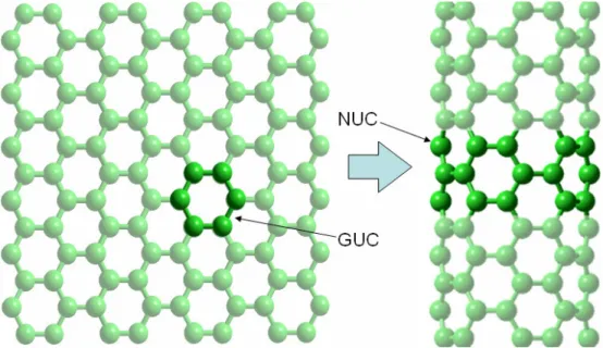
CNTs are three-dimensional carbon molecules that are a member of the fullerene structural carbon family. To understand the structure of a CNT it is necessary to discuss the structure of graphene. Graphene, a single plane of graphite, exists as a planar sheet of carbon atoms whose lattice consists of hexagonal graphene unit cells, as shown in Fig. 2.1. The hexagonal structure means that each carbon atom is bonded aromatically to its neighboring atoms via sp2 hybridized bonds. The spacing between the graphene unit cells, aguc, is 0.246 nm
[36], which corresponds to an equilibrium C-C bond length, ac-c,of 0.142 nm, less than the C-C
bond length found in diamond of 0.154 nm [36]. This sp2 bond configuration produces some of the strongest materials found in nature. Each carbon atom is bonded to three other carbon atoms via σ bonds with 120o of spacing. The carbon atom’s fourth valence shell electron forms a delocalized π bond which is oriented perpendicular to the plane of carbon-carbon σ bonding. This bond configuration leads to a lattice energy of 7.4 eV per atom [37], which is 37% higher than the lattice energy of diamond, 5.4 eV per atom [38].
Figure 2.1: Graphene sheet to CNT analogy.
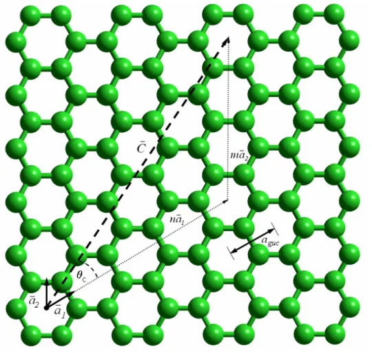
A CNT may be thought of as a sheet of graphene rolled along a chiral vector, Cr, as shown in Fig. 2.1. The chiral vector is a linear combination of two base vectors, av1 and av2,
which are oriented 60o from each other, as shown in Fig. 2.2. The chiral vector is defined using the chiral indicies (n,m) and the relation presented in Eq. 2.1.
2 1 ma a n C v v v + = (2.1)
The chiral vector also defines the diameter, dcnt, of a carbon nanotube, as shown in Eq. 2.2.
π 2 2 nm m n a dcnt = guc + + (2.2)
The energy per atom required to roll a graphene sheet into a CNT, Ur, is inversely proportional to
the square of the CNT diameter [36], as shown in Eq. 2.3.
2 2 3 24 3 cnt guc g g r d a t E U = (2.3)
For this formulation the elastic modulus of graphene, Eg, is 1.06 TPa [36] and the thickness of
the graphene sheet, tg, is 0.34 nm [36]. The wrapping angle, θc, that the chiral vector makes with
basis vector av1 is found using the relation shown in Eq. 2.4.
+ = − n m m c 2 3 tan 1 θ (2.4)
Figure 2.2: Chiral vector definition on a graphene sheet.
The chiral indices also have a large effect on the electrical properties of CNTs. The difference of the indicies of CNTs that behave like conductors, referred to as a “metallic” tubes, are always an integer, q, multiple of three, as shown in Eq. 2.5.
,... 2 , 1 , 0 where 3q= n−m q= (2.5)
Any other index pair indicates the tube is semiconducting with an energy bandgap, Ugap, that is
proportional to a hopping parameter, ζ, (usually 2.5-3.2 eV) as is shown in Eq. 2.6 [11].
cnt guc gap d a U = ζ (2.6)
Finally, the chiral indicies lead to three types of nanotubes: 1) zig-zag (Fig. 2.3(a)), 2) armchair (Fig. 2.3(b)), and 3) chiral. Zig-zag CNTs have m = 0, leading to a wrapping angle of 0o and
diameters that are directly proportional to n. Armchair nanotubes have a repeated index (m = n),
leading to diameters proportional to 3 and wrapping angles of 30n o. This bounds the third class of CNTs, which includes all the other combinations of indicies, to have wrapping angles between 0o and 30o.
(a) (b)
Figure 2.3: Zig-zag (a) and armchair (b) carbon nanotube chiralities1.
Once a chiral vector is defined, it becomes necessary to introduce the idea of a nanotube unit cell. The nanotube unit cell, shown in Fig 2.1, is a single cylindrical building block of a CNT. A CNT is formed by stacking unit cells on top of one another, thus making the length of a CNT, Lcnt, an integer multiple of the nanotube unit cell height, Tnuc. The nanotube unit cell height
depends solely on the indicies of the CNT, as shown in Eq. 2.7.
(
)
R guc nuc d m nm n a T 2 2 3 + + = (2.7)The variable in the denominator of Eq. 2.7, dR, is itself a function of the greatest common divisor
(gcd) of m and n and its definition is given in Eq. 2.8.
( m n n m)
dR =gcd2 + ,2 + (2.8)
One may also find the number of graphene unit cells, Nguc, per nanotube unit cell using the
relation shown in Eq. 2.9.
(
)
R guc d m nm n N 2 2 2 + + = (2.9)Since each graphene unit cell is defined by two carbon atoms, the total number of atoms per nanotube unit cell is 2Nguc.
It is important to distinguish between single-walled carbon nanotubes (SWCNTs) and multi-walled carbon nanotubes (MWCNTs). MWCNTs consist of multiple SWCNTs that are
1 Figure 2.3 reproduced by permission from Elsevier: C. Li and T.W. Chou. Int. J. Sol. and Structures 40 (10), 2487
coaxially nested. Each wall of the MWCNT may have a different chirality, though these chiralities are usually complementary matched in order to minimize the non-bonded energy between the walls of the MWCNT. The walls are usually spaced 0.341 nm apart, which is the interlayer spacing of graphene layers in graphite [36], though Kiang et. al has found that the wall separation is inversely proportional to the number of layers in the MWCNT and directly proportional to the curvature [40]. The nested structure of a MWCNT allows it to reach diameters of up to 100 nm, while SWCNTs are usually limited to 5 nm or less. Furthermore, the non-bonded interactions between the walls of the MWCNT lead to changes in their mechanical properties, in many cases making them approach that of graphite. This is because graphite is structurally similar to a deck of cards, i.e. it is a stack of graphene sheets.
The two most common ways to destroy the structure of a CNT under load is via bond breaking or defect formation. In order to break an atomic bond the C-C bond length must be stretched to 0.177 nm [41], corresponding to 25% bond strain. It is also possible for a CNT wall to develop defects caused by bond rotations, which is the more common type of CNT failure. This type of failure occurs when four clustered hexagonal graphitic unit cells recombine to form two pentagons and two heptagons, as shown in Fig. 2.4, and is known as a Stone-Wales deformation.
Figure 2.4: Stone-Wales defect in a SWCNT 2.
In simulations of a SWCNT in axial tension, Nardelli, Yakobson, and Bernholc found that reversible defects occur at 5% extension [42]. The Stone-Wales deformation is a method of relieving strain energy in the wall of the CNT. Nardelli found that at 10% strain the presence of a defect lowered the strain energy of the SWCNT by 1.77 eV when compared with the defect-free configuration at the same loading level [42]. This is because the heptagons are capable of
2 Figure 2.4 reproduced with permission from M.B. Nardelli, B.I. Yakobson, and J. Bernholc. Phys. Rev. B 57 (8),
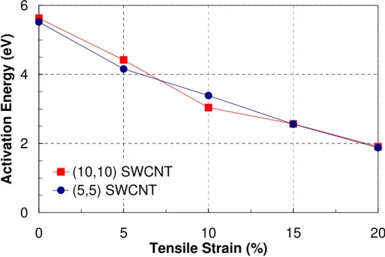
straining the same amount as a hexagon without making each individual C-C bond as long as they would be in the hexagon. Nardelli also provided simulated results for the activation energy of a defect, which decreases as the SWCNT is loaded. The results of the study are presented in Fig. 2.5.
0
2
4
6
0
5
10
15
20
Tensile Strain (%)
A
c
ti
v
a
ti
o
n
E
n
e
rg
y
(
e
V
)
(10,10) SWCNT
(5,5) SWCNT
Figure 2.5: Activation energy for a Stone-Wales defect in a SWCNT.
It is important to note that while these Stone-Wales deformations may be reversible under ideal conditions, it is possible for them to serve as nucleation sites for plastic deformation (i.e. dislocations) in the wall of the SWCNT.
2.2 Physical Properties of Carbon Nanotubes
As discussed in section 2.1, the aromatic carbon bonds present in the nanotube are stronger than the sp3 bonds present in diamond, which is why CNTs possess such unique mechanical properties. The atomic structure of a CNT also leads to interesting kinematic and elastomechanic phenomenon such as buckling and bi-stable geometries. This section will focus on the mechanical properties associated with axial, bending, and torsional deformations.
2.2.1 Continuum Definitions of Mechanical Properties at the Nano-scale
Before any discussion of mechanical properties of CNTs may begin, it is important to note the problems associated with using continuum descriptions of macro-scale mechanical properties at the nano-scale. All macro- and micro-scale continuum relations assume that a cross-sectional area or moment of inertia may be provided for the structure. Since a CNT is really a planar structure only one atom in thickness, it becomes difficult to prescribe a continuum thickness to the structure. In the sections to follow we will see that some authors choose to define the thickness of a CNT, tcnt, as the equilibrium van der Waals spacing between graphene
sheets while others choose to make the thickness of the CNT equal to the diameter of a carbon atom. To further complicate matters, some authors define the cross-sectional area of a carbon nanotube to be a solid rod, while others model it as a hollow cylinder. Harik has proven by geometric similitude that a SWCNT may be considered a thin-walled cylindrical shell, a thick-walled cylindrical shell, or a solid rod based on five unique ratios [43]. The inability to define a thickness of a CNT also leads to trouble with establishing its mass in a macro-scale sense. While the bulk density of CNTs is known to be 2020 kg/m3 [44], defining the mass of an individual CNT is best done by adding the mass of each individual atom in the structure rather than defining a local density and volume. In order to alleviate this confusion, whenever an elastic modulus is quoted the diameter of the CNT as well as the assumed thickness will also be provided. Another value that will be quoted will be the product E⋅tcnt, which may be thought of
as an in-plane stretching stiffness for a CNT cross-section for the CNT cross-section. We will see in the next section that this product will be important for comparing data from different published studies.
2.2.2 Properties of Axial Deformation
Due to the sp2 structure of the carbon nanotube, the σ bonds in plane tend to make the CNT quite stiff in the axial direction, while compliant in the tangential direction. Much simulation and experimental work has been conducted in order to predict the elastic modulus, E,
Poisson’s ratio, ν, and failure strength, σf, and failure strain, εf, for axially loaded CNTs. It will
become important to distinguish between axial elongation and compression because the elastomechanic behaviors exhibited in both are quite different. Table 2.1 details the simulated and experimental results found in the literature for the elastic properties of CNTs in tension.
From the published literature, the elastic modulus for a SWCNT has an average value of 1.32 TPa. In contrast the MWCNT elastic modulus seems to approach that of graphite with its approximate value of 1 TPa.
Table 2.1: Elastic properties of CNTs in axial extension.
Test Type Tube Type Chirality dcnt (nm) Lcnt (nm) tcnt (nm) E (TPa) ν E⋅tcnt
(nN/nm) Ref.
Simulation SWCNT (9,0) 0.71 N/A 0.34 1 N/A 340 [39]
Simulation SWCNT (10,10) 1.36 N/A 0.34 1.24 N/A 422 [45] Simulation SWCNT (25,0) 1.96 N/A 0.129 1.44 N/A 186 [46] Simulation SWCNT (10,10) 1.36 2.48 0.0894 3.86 0.149 345 [47] Simulation SWCNT (10,10) 1.36 N/A 0.34 0.973 0.28 331 [48] Simulation SWCNT N/A 1.12 N/A 0.286 1.024 0.16 293 [49] Simulation SWCNT (10,10) 1.36 N/A 0.34 0.8 0.14 272 [50]
Simulation MWCNT N/A 4 N/A 0.34 1 N/A N/A [50]
Experiment SWCNT N/A 1 5 0.154 0.950 N/A 146 [51]
Experiment SWCNT N/A 1.36 N/A 0.34 1 N/A 340 [52]
Experiment MWCNT N/A 30 N/A 0.34 0.95 N/A N/A [53]
It is because of the variation in the assumed wall thickness (from 0.34 nm to 0.068 nm) that the elastic modulus of a SWCNT cannot be considered a constant. A better constant for a SWCNT is the product E⋅tcnt, whose constant value may be considered to be 297 nN/nm with a standard
deviation of 85 nN/nm. The Poisson’s ratio for a SWCNT in axial tension has an average value of 0.18.
Simulated and experimental work has also been conducted to find the approximate failure strength and strain for CNTs in tension. The results of this published research is presented in Table 2.2. The simulated failure stress for a SWCNT is approximately 88 GPa assuming a wall thickness of 0.34 nm, while the simulated failure strain, εf, varies wildly from study to study.
However, there are considerable differences between the experimental and simulated results for the values of SWCNT failure. The average experimental failure stress for a SWCNT is 27 GPa, 70% lower than the simulated results. The experimental failure strain also varies wildly from test to test. This difference between experimental and simulated work could be due to the
presence of defects, which are nearly impossible to detect during these experiments, as well as imperfect sample loading such as a failure to put the CNT in pure tension.
Table 2.2: Failure properties of CNTs in axial extension.
Test Type Tube Type Chirality dcnt (nm) Lcnt (nm) tcnt (nm) σf (GPa) εf Ref.
Simulation SWCNT (30,30) 4.07 N/A 0.334 88 0.443 [3]
Simulation SWCNT (6,6) 0.81 N/A 0.34 87.2 0.073 [41]
Simulation SWCNT (10,0) 0.78 N/A N/A N/A 0.16 [54]
Simulation SWCNT (5,5) 0.68 N/A N/A N/A 0.24 [54]
Experiment SWCNT N/A 1 5 0.154 25 0.30 [51]
Experiment SWCNT N/A 1.36 N/A 0.34 30 0.053 [52]
Experiment MWCNT N/A 30 N/A 0.34 2.9 0.12 [53]
Another explanation is provided in [41], where the authors have found that the critical failure stress and strain is directly proportional to the rate of strain. Since most of the experimental work in the literature has not provided the rate of strain, it may not be appropriate to use these experimental results for comparison to the simulated tension tests.
Less published research is available on the behavior of CNTs in compression. Table 2.3 shows the simulated and experimental results for axial compression of a CNT. The simulated results for a SWCNT show that the product E⋅tcnt is within the standard deviation of the results
from the axial tension experiments. Furthermore, the simulated Poisson’s ratio for a SWCNT has a value similar to the one found for axial tension.
Table 2.3: Elastic properties of CNTs in axial compression.
Test Type Tube Type Chirality dcnt (nm) Lcnt (nm) tcnt (nm) E (TPa) ν E⋅tcnt
(nN/nm) Ref
Simulation SWCNT (7,7) 0.95 6 0.066 5.5 0.19 363 [55]
Experiment SWCNT N/A 1.4 N/A N/A 3 N/A N/A [56]
Experiment MWCNT N/A 10-20 N/A N/A 2.44 N/A N/A [56]
The main difference between axial compression and tension is that it in compression a CNT is subject to buckling at a critical buckling strain, εc. A visual depiction of compressive
buckling is shown in Fig. 1.8. Researchers have simulated the buckling of SWCNTs with much success. Their results are presented in Table 2.4. From the above table it is easily shown that the
critical buckling strain is highly dependant on nanotube diameter, as one would expect from macro-scale beam theory.
Table 2.4: Failure properties of CNTs in axial compression.
Test Type Tube Type Chirality dcnt (nm) Lcnt (nm) tcnt (nm) εc Ref
Simulation SWCNT (55,0) 4.31 38 0.068 0.0101 [25]
Simulation SWCNT (7,7) 0.95 6 0.066 0.05 [55]
Simulation SWCNT (8,0) 0.63 4.3 0.0894 0.13 [57]
A relationship for the critical buckling strain to SWCNT diameter for tubes with an aspect ratio
Lcnt/dcnt less than ten is presented in Eq. 2.10 [55].
10 for ) nm 077 . 0 ( ≤ = cnt cnt cnt c d L d ε (2.10)
For SWCNTs with greater aspect ratios one should use the formulation [55] presented in Eq. 2.11. 10 for 2 1 2 2 2 ≥ = cnt cnt cnt cnt c d L L d π ε (2.11)
For small diameter SWCNTs, Liew et. al [57] have related the critical buckling load to the classical Euler beam buckling formulations, as shown in Eq. 2.12. The moment of inertia, I, is
considered to be that of a solid rod and E is taken to be 1.28 TPa.
nm 03 . 1 for 4 2 ≤ = cnt c d L EI P π (2.12)
It has also been shown [25] that the buckling of an SWCNT is bistable if the CNT is 2-6 nm in diameter. If the tube is any larger than 6 nm, the van der Waals forces dominate the buckled geometry, and the buckling event is not reversible. It was shown that a 38 nm long (55,0) SWCNT would need 1.01% compressive strain to buckle, and 1.29% tensile strain to revert back to an unbuckled geometry [25].
2.2.3 Properties of Bending Deformation
CNTs undergoing bending deformation represent the largest range of elastic motion that is offered in nature. Since this large range of motion depends on the geometric nonlinearity of the CNT in large-angle bending, it is necessary to separate the discussion of SWCNTs and MWCNTs. Table 2.5 summarizes the experimental and simulated mechanical properties of SWCNTs found in the literature. When the wall thickness is taken to be approximately 0.08 nm, the elastic modulus is approximately 4.9 GPa. The product E⋅tcntis again found to be a constant
equal to 382 nN/nm with a standard deviation of 41 nN/nm. This is a higher value than previously determined in the tension/compression studies, and a t-test between the two data sets confirms that this difference is statistically significant with 98% confidence. This result suggests that SWCNTs experiencing combined loading may possess an elastic modulus that is a combination of the stretching and bending moduli.
Table 2.5: Elastic properties of SWCNTs in bending.
Test Type Tube Type Chirality dcnt (nm) Lcnt (nm) tcnt (nm) E (TPa) ν E⋅tcnt
(nN/nm) Ref Simulation SWCNT (5,5) 0.68 N/A 0.074 5.1 0.24 377 [58]
Simulation SWCNT N/A N/A N/A 0.075 4.7 0.34 353 [59]
Simulation SWCNT (13,0) 1.02 8 0.075 4.84 0.19 363 [60]
Experiment SWCNT N/A 3.1 605 0.34 1.2 N/A 408 [61]
Experiment SWCNT N/A 5 N/A N/A 1.2 N/A N/A [62]
Experiment SWCNT N/A 1.5 36.8 0.34 1.33 N/A 452 [63]
Experiment SWCNT N/A 1.4 N/A 0.34 1 N/A 340 [64]
Experiment SWCNT N/A 3 1040 0.34 1.31 N/A 445 [65]
The difference in the stretching and bending moduli is attributed to the method of bond deformation in the CNT. During axial loading, bonds tend to be stretched while in a bent CNT the bonds tend to rotate relative to each other to minimize energy in the structure. This is possible because in bending the cross-section of a CNT deforms from a circle into an oval, while in an axial loaded CNT the cross-section remains constant.
It is important to note that at a critical angle the SWCNT transitions from distributed beam bending to localized bending creating a kink in the CNT. This kink that forms during tube buckling allows the large motion bending that is seen in simulated and experimental SWCNT tests, as shown in Fig. 2.6. Pantano, Parks, and Boyce found that the large-angle bending was reversible until the SWCNT diameter exceeded 6 nm [60], at which point the van der Waals forces dominated the elasticity of the atomic lattice and the SWCNT would not come unkinked. For smaller diameter SWCNTs it has been shown that the bending angle may approach 110o and the SWCNT will revert back to its original undeformed state [66].