HAL Id: hal-00383348
https://hal.archives-ouvertes.fr/hal-00383348
Submitted on 13 May 2009
HAL is a multi-disciplinary open access archive for the deposit and dissemination of sci-entific research documents, whether they are pub-lished or not. The documents may come from teaching and research institutions in France or abroad, or from public or private research centers.
L’archive ouverte pluridisciplinaire HAL, est destinée au dépôt et à la diffusion de documents scientifiques de niveau recherche, publiés ou non, émanant des établissements d’enseignement et de recherche français ou étrangers, des laboratoires publics ou privés.
Size effects on varistor properties made from zinc oxide
nanoparticles by low temperature spark plasma sintering
Lena Saint Macary, Myrtil L. Kahn, Claude Estournès, Pierre Fau, David
Trémouilles, Marise Bafleur, Philippe Renaud, Bruno Chaudret
To cite this version:
Lena Saint Macary, Myrtil L. Kahn, Claude Estournès, Pierre Fau, David Trémouilles, et al.. Size effects on varistor properties made from zinc oxide nanoparticles by low temperature spark plasma sintering. Advanced Functional Materials, Wiley, 2009, 19 (11), p.1775-1783. �hal-00383348�
Size effects on varistor properties made from zinc oxide nanoparticles
by low temperature spark plasma sintering
By Léna Saint Macary, †§ Myrtil L. Kahn,†* Claude Estournès;‡ Pierre Fau†, David
Trémouilles,¤ Marise Bafleur,¤ Philippe Renaud,§ and Bruno Chaudret†*
† Dr. B. Chaudret, Dr. M. Kahn, Dr. P. Fau, L. Saint Macary
Laboratoire de Chimie de Coordination, UPR8241 CNRS,
205 route de Narbonne, F-31077 Toulouse, France
E-mail : kahn@lcc-toulouse.fr, chaudret@lcc-toulouse.fr
‡ Dr. C. Estournès
Centre Interuniversitaire de Recherche et d’Ingénierie des Matériaux & Plateforme Nationale
de Frittage Flash, Module de Haute Technologie, Université Paul Sabatier,
118 route de Narbonne, F-31062 Toulouse, France
§ Dr. P. Renaud, L. Saint Macary
Freescale Semiconductor,
134 avenue du Général Eisenhower, F-31023 Toulouse, France
¤ Dr. M. Bafleur, Dr. D. Trémouilles
LAAS-CNRS, Université de Toulouse,
ABSTRACT:
Conditions for the elaboration of nanostructured varistors by Spark Plasma Sintering (SPS)
are investigated, using 8 nm zinc oxide nanoparticles synthesized following an organometallic
approach. A binary system constituted of zinc oxide and bismuth oxides nanoparticles is used
for this purpose. It is synthesized at room temperature in an organic solution through the
hydrolysis of dicyclohexylzinc and bismuth acetate precursors. Sintering of this material is
performed by SPS at various temperatures and dwell times. The determination of the
microstructure and the chemical composition of the as prepared ceramics are based on
Scanning Electron Microscopy (SEM) and X-Ray Diffraction (XRD) analysis. The non linear
electrical characteristics are evidenced by current-voltage (I-V) measurements. The
breakdown voltage of these nanostructured varistors strongly depends on grain sizes. The
results show for the first time that, nanostructured varistors are obtained by SPS at sintering
temperatures ranging from 550 to 600°C.
1. Introduction
Zinc oxide (ZnO) is characterized by remarkable optical, thermal, electronic and chemical
properties. It is a wide band gap (3.37 eV at room temperature) II-VI n-type semiconductor
displaying many applications, from solar cell electrodes,[1] which take advantage of both its
optical transparency in the visible range and conductivity in thin film form, to the exploitation
of high electromechanical coupling constant values as piezoelectric transducers.[2] ZnO
remains the subject of many research works. A central issue consists in doping this material;
first because p-doping is a prerequisite for its use in optoelectronics and also because
obtaining an experimental proof of the calculated ferromagnetism at room temperature of
ZnO doped with 3d transition metals is still a challenging issue.[3] Among these present and
future applications, ZnO ceramics associated with other additive oxides are well known to
work as varistors, i.e. these are devices which exhibit non-linear current-voltage (I-V)
characteristics.[4, 5] Such micrometric ZnO-based varistors are widely employed and
commercialized to protect electrical equipments operating at various voltage levels from
degradations caused by overvoltage peaks and electrostatic discharges such as the ones related
to lightning events in aeronautics applications.
From a practical point of view, it is usually accepted that the protection voltage is
proportional to the number of grain boundaries.[6] The expansion of nanoscience over the last
decades stimulated chemists so that a wide variety of nanoobjects were developed and are
now available by the so called bottom-up approach.[7] Such structures have attracted much
interest in the varistor world for the design of high quality devices since size and
microstructure control are key parameters for the elaboration of non linear ceramics.[8] They
proved useful to improve electrical characteristics, in particular breakdown field. However
such polycrystalline materials usually undergo a growth of their grain size during sintering[9]
diameter grain size below 100 nm (nanostructured varistors) have been reported. The finest
grained varistor ceramics described in the literature contain grains in the range of 250 to 500
nm in diameter.[10, 11] The aim of the present study is therefore to explore new process
allowing the realization of nanostructured varistors.
Here is reported the use of ZnO nanoparticles synthesized by an organometallic method for
the design of nanostructured varistors. This method allows a good control over the size and
surface state of the particles. In the present work, the most widespread varistor forming oxide,
namely bismuth oxide (Bi2O3), is the only added constituent for the manufacture of ceramic
parts. They are thus expected to exhibit only low non linearity coefficients. Interestingly, the
nanometric scale of the grains was preserved by the use of a non conventional sintering
technique: Spark Plasma Sintering (SPS).
2. Experimental part
2.1. Synthesis:
Pure zinc oxide materials:
Two equivalents of water were added dropwise to a 4.32 M THF solution of [ZnCy2]
via a wet solution of THF containing 10300 ppm of water. After the solution turned dark
yellow, a white solid precipitates within minutes. THF is evaporated to dryness under
vacuum. A white powder is obtained.
Zn/Bi mixed metal oxide materials:
A 0.08 molar equivalent of bismuth triacetate (III) were added to a 4.32 M THF
solution of [ZnCy2]. The solution is kept under stirring during 10 minutes in order to achieve
the complete dissolution of bismuth triacetate (III). Two equivalents of water were then added
dropwise. The solution turns yellow then white and a precipitate forms. The powders were
2.2. XRD:
The powder's and pellet's X-ray diffraction patterns were collected on a XPert Pro
(Theta-Theta mode) Panalytical diffractometer with λ(CuKα1, Kα2) = 1.54059, 1.54439 Å,
respectively. The extraction of peak positions for indexing was performed with the fitting
program, available in the PC software package Highscore+ supplied by Panalytical. The phase
identification was performed with 'searchmatch' in Highscore+, based on the PDF2 ICCD
database.
2.3. TEM/SEM:
The TEM specimens were prepared by slow evaporation of solution droplets of the
different samples deposited on carbon-supported copper grids. The experiments were
performed on a JEOL JEM-1011.
The size distribution was determined manually by an analysis of low-magnification
TEM images. In this procedure, the different particles were visually identified according to an
upper and lower intensity threshold and then counted and measured. This analysis was made
only on isolated particles which are not numerous in the case of agglomerated particles, thus
giving only an estimate of the particle size.
SEM specimens were prepared as follows: the powder samples were either deposited
on a silicon substrate or glued directly on the aluminum sample holder via a silver paste.
Pellets were directly stuck to the aluminum sample holder by a carbon-double-face tape. SEM
measurements were performed on a field emission gun scanning electron microscope JEOL
6700F. Micrographs were collected using secondary electron imaging (SEI) for the
X-ray analysis was performed using the SEM interfaced with a Princeton Gamma-Tech energy
dispersive X-ray (EDX) microanalysis system.
2.4. Sintering:
Classical sintering:
Pellets were prepared by uniaxial pressing ZnO powders in a 5 mm diameter die.
Usual sintering process under air was performed in a compact tube furnace RS50/300/11 from
Nabertherm equipped with a C40 program controller at a maximum temperature ranging from
850 to 1000°C. The heating rate from room temperature to 400°C is 1°C.min-1; above 400°C
the temperature is raised by 2°C.min-1 up to the maximum temperature which is held for 2h.
The cooling rate is 1.5°C.min-1.
Spark Plasma Sintering:
Samples were sintered using a Dr Sinter 2080 SPS apparatus (SPS Syntex Inc., Tokyo,
Japan). Precursor’s powders (without any sintering aids) were loaded onto an 8-mm inner
diameter cylindrical die and placed in a chamber under vacuum. The pulse sequence was 12-2
(pulses–dead time or zero current), with each pulse lasting 3.3 ms. The temperature was
automatically raised from room temperature, monitored and regulated to the final temperature
(500-800°C range) by thermocouple introduced in a small hole located at the surface of the
die. A heating rate of 50°C.min-1 was used to reach the final temperature. The cooling
conditions are not forced: once the maximum temperature is reached, heating is stopped and
the pellets are left to cool down to room temperature. Uniaxial pressure of 50 MPa was
applied progressively in the first minute and held until completion of the temperature step at
final temperature (held from 0 to 15 minutes). In these conditions, the current passing through
the die and the voltage reached maximum values of applied values of 300 A and 3 V,
2.5. Electrical measurements:
The sintered pellet surfaces were polished using various grades of SiC abrasive papers
(Presi P600 and P1200) down to a thickness of about 1 mm in order to eliminate the carbon
surface contamination induced by the use of graphitic dies. Gold electrodes were further
deposited on both sides of the pellets by sputtering on an Alcatel 450 sputtering machine.
Electrical measurements were performed on a HP4142B Modular DC Source Monitor limited
to 200 V in absolute value. These measurements were completed when necessary on a 370A
Programmable Curve Tracer from Sony Tektronix attaining 2000 V.
3. Results
3.1 Synthesis:
In order to test the effect of bismuth oxide addition on zinc oxide based ceramics, we
first synthesized nanometric zinc oxide powder as a reference sample. This was achieved by
decomposition of an organometallic precursor in solution, namely the dicyclohexyl zinc
compound, [ZnCy2], in THF. The precursor is hydrolyzed by controlled introduction of water
in the solution kept under argon. If only one equivalent of water is added to the reaction
medium, a yellow air sensitive precipitate forms which turns white when placed in contact
with air or upon addition of another equivalent of water. Two equivalents of water are
necessary to complete the direct formation of the final white ZnO product in solution. Once
the solvent was removed by evaporation under vacuum, the white solid (Sample 1) was
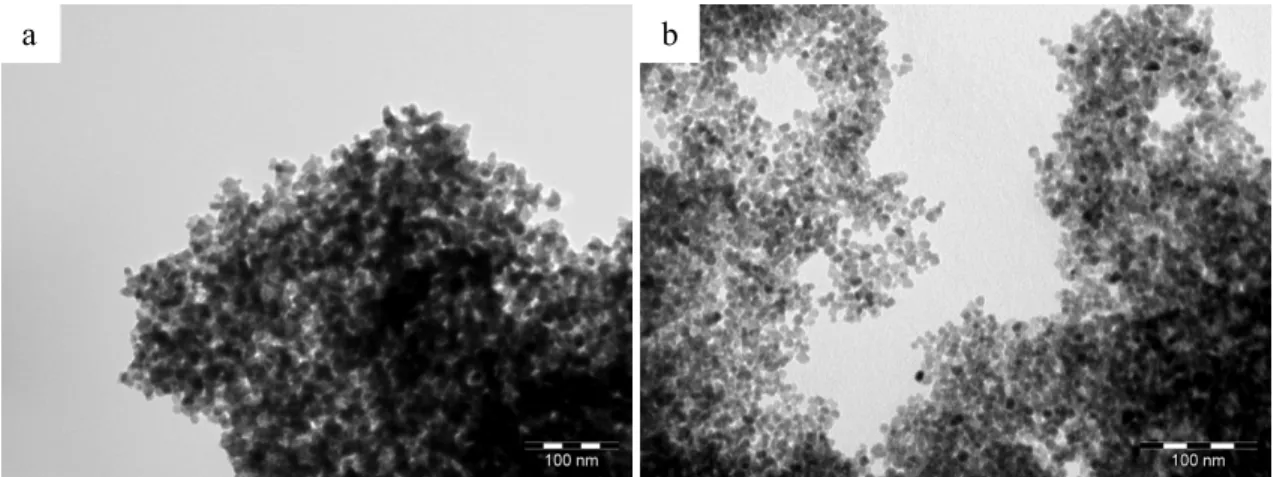
characterized by TEM as agglomerated nanoparticles (see Figure 1a) of approximate diameter
10 nm.
Bismuth oxide is known as one of the so-called varistor forming oxides when
bismuth atoms at the interfaces between zinc oxide grains.[12] Consequently, we focused on
granting the homogeneous distribution of bismuth at the nanometric scale in the synthesized
powders. Thus, we performed the codecomposition of the same organozinc precursor and a
bismuth salt, namely bismuth acetate, in a one step controlled hydrolysis. The intermediate
yellow product discussed hereabove also forms. The obtained particles (Sample 2) are similar
in size and shape with Sample 1 ones, but these two samples differ in terms of agglomeration.
Sample 2 is composed of well-defined isotropic nanoparticles (see Figure 1b).
Figure 1: TEM micrographs of nanoparticles syntheses of: a) Sample 1; b) Sample 2
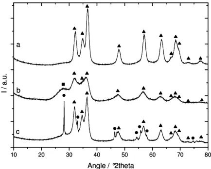
XRD characterization of the as-obtained powders identifies both for Sample 1 and
Sample 2, a würtzite zinc oxide phase (see Figure 2a and 2b respectively). The extent of the
crystalline domains is larger in Sample 1 than in Sample 2. Sample 2 diffractogram shows an
additional peak situated around 30° corresponding to bismuth. However, no clues are given
concerning the phase under which bismuth is found since the peak is too broad to be analyzed.
In order to gain access to more information concerning this phase, the hydrolysis of bismuth
acetate alone in THF was performed and the resulting white powder analyzed by XRD. The
diffractogram indicated the presence of bismuth oxoacetate and unreacted bismuth acetate
(see supplementary materials, S1). It is however difficult to conclude on the presence or not of
bismuth acetate in this case. Indeed, the most intense peak of bismuth oxide in its beta phase
is also situated at similar angle values. High resolution transmission electronic microscopy
(HRTEM) was performed on Sample 2 but the bismuth based phase was not located. Once
dried, the nanoparticles of Sample 2 were submitted to post-synthesis annealing treatment at
400°C for 4h (Figure 2c). All the diffractograms display characteristic peaks of the hexagonal
zincite phase (space group P63mc) in the 30° to 80° 2θ range. These peaks have narrowed
indicating crystallite growth. Additional peaks appeared; and were clearly identified as
bismuth oxide in the beta allotropic form (Figure 2c). The width of the corresponding peaks
suggests that the β-Bi2O3 crystallites are larger than zinc oxide ones.
10 20 30 40 50 60 70 80 I / a .u . c b Angle / °2theta a 10 20 30 40 50 60 70 80 I / a .u . c b Angle / °2theta a
Figure 2: X-Ray diffractograms: a) Sample 1 as prepared; b) Sample 2 as prepared; and c)
S1: X-Ray diffractogram of the product obtained by direct hydrolysis of bismuth acetate
3.2. Sintering:
The next step consisted in making dense nanoceramics from these nanostructured
powders in order to study their electrical characteristics. Attempts to sinter pure ZnO
nanopowders (Sample 1), once shaped into pellets by pressing at 3 tons, were first carried out
in a furnace at temperatures ranging from 800 to 1000°C for 2h. The as-prepared pellets are
highly porous, their densities hardly reach 30% of pure zinc oxide (figure 4a). A second
technique, namely spark plasma sintering (SPS), was considered. It consists in hot pressing at
very high heating rates. Various final temperatures and holding times were tested both for the
reference powder (Sample 1) and bismuth containing powder (Sample 2). The experimental
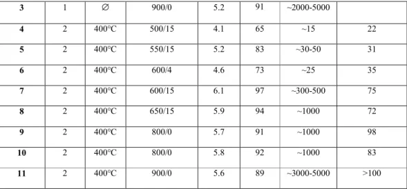
conditions are summarized in Table 1.
Pellet Sample
Sample annealing
Sintering Tmax[°C]
/Step time [min]
Density [g.cm-3] Density [%] SEM Grain size [nm] XRD cristallite size [nm] 1 1 ∅ 600/0 3.8 67 ~10 2 1 ∅ 800/0 4.7 82 ~100 10 20 30 40 50 60 70 80 I / a .u . Angle / °2 Theta
3 1 ∅ 900/0 5.2 91 ~2000-5000 4 2 400°C 500/15 4.1 65 ~15 22 5 2 400°C 550/15 5.2 83 ~30-50 31 6 2 400°C 600/4 4.6 73 ~25 35 7 2 400°C 600/15 6.1 97 ~300-500 75 8 2 400°C 650/15 5.9 94 ~1000 72 9 2 400°C 800/0 5.7 91 ~1000 98 10 2 400°C 800/0 5.8 92 ~1000 83 11 2 400°C 900/0 5.6 89 ~3000-5000 >100
Table 1 : Data of the pellets prepared by SPS
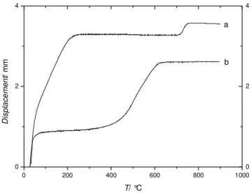
During SPS, thermal shrinkage is monitored by a dilatometer, which allows to get
insights on the sintering process. Sintering profiles considerably differ depending on the
powder composition as illustrated in Figure 3. For example, Sample 1 densification occurs
between 700 and 750°C (Figure 3a), whereas bismuth containing powder (Sample 2)
undergoes significant shrinkage at lower temperatures, between 400 and 650°C (Figure 3b).
The important displacement observed at low temperature for Pellet 2 compared to Pellet 11 is
mainly due to the fact that initial compaction prior to SPS is carried out manually. The fact
that Sample 1 was not annealed prior to sintering may also partly explain this difference as the
amount of adsorbed species may be higher in this case.
Final densities of the pellets were measured using the water immersion method. Pellets
made from Sample 1 are all the more dense as the applied temperature is high. A densification
of 90% of the theoretical density of zinc oxide (5.7 g.cm-3) was reached at the maximum
temperature of 900°C applied for this study. For Sample 2, it can be noted that the theoretical
density (6.4 g.cm-3) is higher than that of pure zinc oxide due to the amount of bismuth oxide.
The trend concerning the variation of density with temperatures for this composition (Sample
increases with the sintering temperature increase. Indeed, for Sample 2, pellets made at 800°C
are denser than the ones sintered at 900°C (Table 1). Moreover, a step at final temperature for
several minutes was found to have a considerable impact on sintering, yielding very high
densities at temperatures as low as 600°C.
0 200 400 600 800 1000 0 2 4 0 2 4 a b T/ °C D is p la c e m e n t/ m m
Figure 3: Sintering profiles of: a) Pellet 2 made from Sample 1; b) Pellet 11 made from
Sample 2
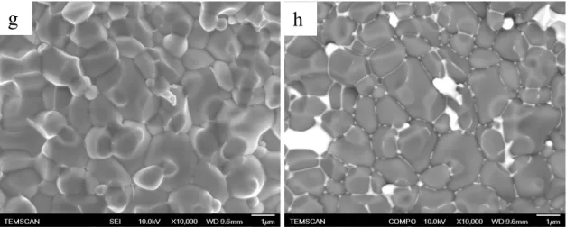
The pellets’ microstructure was observed by SEM. Figure 4(a-g) shows characteristic
SEM images of ceramics sintered from Sample 1 and Sample 2 at various temperatures.
Pellets prepared from Sample 1 by SPS at 800°C considerably differ from those sintered in a
classical furnace at 1000°C in terms of density (4.7 and 1.7 g.cm-3 respectively), their grain
sizes, however are similar and about a few hundred nanometers as shown in Figure 4a and 4b.
Grain size increase with temperature is observed for each powder composition. For
example, Pellet 1 grains, corresponding to the sintering of Sample 1 at 600°C (Figure 4b), are
in the range of a few tens of nanometers whereas Pellet 2 and Pellet 3, which were also made
from Sample 1, exhibit grains of about 100 nm and 1 µm respectively as a result of SPS
containing samples. In the case of Sample 2, SPS sintering at 600°C (Pellet 6) and at 800°C
(Pellet 10) yields grains of about 50 nm (Figure 4f) and 1 µm (Figure 4g) respectively. Grain
size and density are also considerably modified with dwell time, as illustrated at 600°C by the
difference between Pellet 6 and Pellet 7 maintained at the final temperature for 4 and 15
minutes, respectively. A grain size increase of an order of magnitude occurs and is associated
with an increase in density in Pellet 7, globally resulting from a decrease in porosity (see
Table 2). In micrometric ceramics, bismuth-rich phases are generally found to be located at
multiple grain boundaries.[13, 14] Backscattered Electron Imaging (BEI) micrographs (Figure
4g) provide a view of the repartition of the elements in the pellets by chemical contrast
imaging. Bismuth-rich phases appear in white and zinc oxide in gray, which is evidenced by
X-ray microanalysis (see supplementary material, S2). This method shows that in pellets
sintered by SPS at high temperature, thus undergoing grain growth up to the micrometric size,
bismuth is mainly found to stand at the multiple grain junctions (Figure 4h). Some grain
junctions exhibit larger amounts of bismuth, but the distribution of bismuth inside the material
appears homogeneous. For Pellet 5 and Pellet 6, BEI can not be performed at these
magnifications however two phases can be distinguished. It can be assumed that polyhedral
well faceted grains correspond to zinc oxide, the second interpenetrated phase being identified
a
b
c
d
Figure 4: SEM SEI micrographs of fracture surface of: a) Sample 1 sintered at 1000°C in a
furnace; b) Pellet 2, Sample 1 sintered by SPS at 800°C; c) Pellet 3, Sample 1 sintered by SPS
at 900°C; d) Pellet 1, Sample 1 sintered by SPS at 600°C; e) Pellet 5, Sample 2 sintered by
SPS at 550°C for 15 minutes; f) Pellet 6, Sample 2 sintered by SPS at 600°C for 4 minutes; g)
Pellet 10, Sample 2 sintered by SPS at 800°C; h) SEM BEI micrograph of the same image as
(g)
+
+
2
1
+
+
2
2
1
1
g
h
S2: EDX analysis on a backscattered image of: 1) a white zone and 2) a dark zone
Figure 5 shows the XRD diagrams of pellets sintered by SPS at various temperatures.
All diffractograms display the characteristic pattern of zincite phase in the 30° to 60° 2θ
range. Additional peaks result from the presence of bismuth containing phases or surface
carbon contaminants (at 26.5 and 54.5°), this contamination comes from the SPS die and is
further eliminated by polishing. When Pellet 4 is formed by sintering at 500°C for 15 minutes,
a phase transformation of bismuth oxide occurs from beta in the pristine annealed powder to
alpha phase in the pellet (Figure 5a). At higher temperature, namely 600°C, bismuth oxide has
further transformed into γ-Bi2O3 or Bi38ZnO58 (19Bi2O3:ZnO) and two other new species
which are identified as metallic bismuth : one is rhombohedral (R-3m) and the other is cubic
(Pm-3m). The phases γ-Bi2O3 and Bi38ZnO58 have identical crystal structures and can be only
distinguished by a slight shift in the XRD patterns.[15] Consequently, the small intensity and
large width of the corresponding peaks do not allow to discriminate between these two
bismuth oxide phases. At the intermediate temperature of 550°C, a mixture of α-Bi2O3,
γ-Bi2O3 or Bi38ZnO58 and cubic bismuth is found (not shown). As for pellets sintered at 800°C
1
2
and above, bismuth is exclusively present in the rhombohedral metallic phase. The diffraction
peak half-height widths of zinc oxide narrow with sintering temperature as a consequence of
crystallite growth. The crystallite size was estimated using the Debye-Scherrer equation up to
100 nm since above this value the equation is no more valid due to the internal line width of
the diffractometer. These calculations are in good agreement with SEM grain size
observations for finely grained pellets such as Pellet 4, Pellet 5 and Pellet 6. For instance,
Pellet 5 was found to contain 30 nm large crystallites which is the grain size seen on SEM
images (Figure 4e). For pellets made at higher temperatures the crystallite size calculated and
grain size observed do not match; the grain size being larger than the calculated value. This
suggests that the micrometric grains observed by SEM are polycristalline. In order to obtain a
varistor, we annealed the pellets under air so as to turn the metallic bismuth phase into an
oxide phase. This treatment is performed at 650°C for 10h and the temperature is raised at
1°C.min-1. After annealing of these pellets under air at 650°C for 10h (see Figure 4d), metallic
bismuth turned into γ-Bi2O3 or Bi38ZnO58. The main bismuth-rich phase usually found in
varistor ceramics made by classical sintering is the β−Bi2O3 phase,[10, 16] but the presence of δ,
γ and α phases are also reported in some studies depending on the additives and thermal
processing conditions.[17-20] At a temperature of 650°C, bismuth oxide and zinc oxide do not
20 30 40 50 60 I / a .u . Angle / °2theta 20 30 40 50 60 I / a .u . Angle / °2theta
Figure 5: XRD diffractograms for: a) Pellet 4 sintered at 500°C b) Pellet 7 sintered by SPS at
600°C; c) Pellet 9 as sintered at 800°C; and d) Pellet 9 after annealing at 650°C (▲ ZnO, ■ C,
▼ α-Bi2O3, ◊ γ-Bi2O3 or Bi38ZnO58, ● Bi, ○ Bi)
To sum up the results, ceramics are formed by SPS from binary bismuth oxide and
zinc oxide nanostructured powders. After annealing of these powders, sintering is performed
by SPS at low temperature as shrinkage occurs between 400°C and 650°C. By this method,
nanometric grain sized ceramics are obtained between 500 and 600°C. Simultaneously with
densification of the pellets, bismuth oxide undergoes phase transformation into metallic
bismuth. The metallic bismuth phase is turned into the oxide phase again by post sintering
annealing. 3.3. Electrical characteristics: a b c d
Polycristalline ceramics (Pellet 1, Pellet 2 and Pellet 3) prepared from pure ZnO
powder (Sample 1), exhibit linear I/V characteristics with resistivities of about 20 Ω.cm. This
value is slightly higher than that of pure monocristalline zinc oxide, which generally ranges
from 1 to 10 Ω.cm.[21] Pellets prepared from bismuth containing powders (Sample 2) do not
always show non-linear behavior. Indeed, a resistive behavior is observed for pellets that have
not subsequently been annealed under air after sintering. For instance, Pellet 9 and Pellet 10
prepared under the same conditions have radically different electrical behavior as Pellet 10
was not annealed after sintering.
For pellets exhibiting non linear characteristics, following a widespread convention we
determine the breakdown field as the field at which a current density of 1 mA.cm-2 is
measured. The non linearity coefficient α is defined as the slope of the logJ = f(logE) curve
between 1 and 10 mA.cm-2. When the upper value of current density could not be reached, α
was taken as the slope between 1 mA.cm-2 and the last recorded point.
The results of the annealed pellets are reported in Table 2. Some annealed pellets show
linear electrical behavior, namely Pellet 4 and Pellet 11. Their resistivities are also given in
Table 2.
Pellet Tmax [°C] /
step time [min]
Grain size [nm] Cristallite size [nm] α Vb [V.cm-1] ρ [kΩ.cm]
4 500/15 ~15 22 N.A. (non applicable) N.A. 550 5 550/15 ~50 31 NM (non measureable) >19000 N.A. 7 600/15 ~300-500 75 5.8 10660 N.A. 8 650/15 ~1000 72 5.6 10955 N.A. 9 800/0 ~1000 98 3.6 1565 N.A. 11 900/0 ~3000-5000 >100 N.A. N.A. 2
Table 2: Non linear coefficient (α) and breakdown field (Vb) or resistivity of the bismuth
containing ZnO ceramics, annealed after SPS
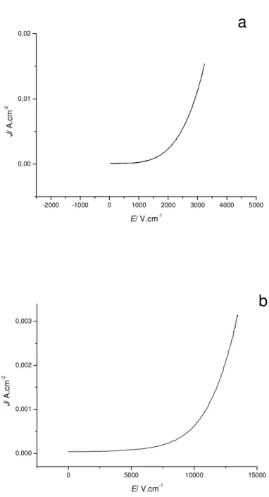
-2000 -1000 0 1000 2000 3000 4000 5000 0,00 0,01 0,02 J / A .c m -2 E/ V.cm-1
a
0 5000 10000 15000 0,000 0,001 0,002 0,003 J/ A .c m -2 E/ V.cm-1b
0 5000 10000 15000 20000 -0,00002 0,00000 0,00002 0,00004 0,00006 0,00008 0,00010 0,00012 J/ A .c m -2 E/ V.cm-1
c
Figure 6: I/V curves of: a) Pellet 9; b) Pellet 8 and c) Pellet 5
Depending on the SPS parameters, pellets annealed after sintering show different
electrical behavior. Pellet 4 and Pellet 11 sintered at 500 and 900°C respectively exhibit a
linear behavior (see supplementary materials, S3) whereas all ceramics sintered at
intermediate temperatures display a non linear varistor behavior (Figure 6). For pellets
exhibiting a non linear behavior, overall alpha values are low as a consequence of the simple
binary composition and range from 3.6 to 5.8. The characteristic breakdown field depends on
grain size observed by SEM, as generally reported. However, there is a discrepancy between
Pellet 8 which has micrometric grain size and a Vb exceeding 10000 V.cm-1 and Pellet 9
which has similar grain sizes but shows a ten times lower breakdown field. This point will be
further discussed. Measurement setup limitation did not allow to extract full electrical
characteristics of Pellet 5. For this pellet, the current density hardly reaches 0.1 mA.cm-2 at
the maximum measurable electric field of 19000 V.cm-1. Therefore, breakdown field and non
behavior is however observed and though current density attained is not sufficient, it can be
asserted that breakdown field is far above 19000 V.cm-1.
-100 -50 0 50 100 -0,0008 -0,0006 -0,0004 -0,0002 0,0000 0,0002 0,0004 0,0006 0,0008 a J / A .c m -2 E/ V.cm-1 -3 -2 -1 0 1 2 3 -0,006 -0,004 -0,002 0,000 0,002 0,004 0,006 b J / A .c m -2 E/ V.cm-1
S3: Electrical characteristics of: a) Pellet 4; b) Pellet 11
4. Discussion
4.1 Synthesis
The synthesis of nanoparticles reported here is an adaptation of the method we previously
described.[22, 23] This reaction involves the hydrolysis of the organometallic precursor [ZnCy2]
in solution. The main improvement consisted in performing a controlled hydrolysis reaction
by adding dropwise an organic solution containing two equivalents of water under inert
atmosphere so as to grant the reproducibility of hydrolysis conditions. Moreover, to meet the
goals of this work, namely the preparation of nanostructured varistors from wet
organometallic chemistry, the synthesis has been developed so as to fulfill the requirements of
the SPS technique. First of all, in order to provide sufficient amounts of material (grams) for
sintering while using reasonable quantities of solvent for the synthesis, the concentration of
the reacting solution is multiplied by more than ten. Finally, we gave up the use of stabilizing
agents such as amine ligands, because they cause the powders to leak out of the SPS die at
possible stabilizing agent is the solvent itself which turns out to be efficient enough to yield
nanoparticles but not to keep them in colloidal state as they agglomerate and precipitate. The
case of Sample 2 which involves the co-hydrolysis of dicyclohexylzinc and bismuth acetate
is, however, somehow different because of the presence of acetate in the reaction solution.
The hydrolysis of the bismuth salt releases acetic acid that may account for the less
agglomerated state of the nanoparticles. Indeed, carboxylic acids are likely to stabilize
nanoparticles synthesized by this organometallic method, since long chain alkyl carboxylic
acids acids are widely employed.[24, 25]
We chose to start our study with the most studied oxides used in the formulation of
varistors, namely zinc and bismuth oxides. Regardless of non linearity coefficient, we
essentially focused on making nanostructured varistors and studying the influence of the
enhanced number of grain boundaries per thickness unit on breakdown field. Usually, the
amount of bismuth oxide used for varistor ranges from 0.5 to 1 mol %.[14, 16, 26] The surface by
volume ratio is considerably higher in the case of nanoparticles when compared to
micrometric powders. Therefore, we adapted the bismuth precursor quantity accordingly and
focused our study on 0.08 molar equivalents of bismuth precursor for the synthesis of the
particles which corresponds to 3.7 mol % Bi2O3.
4.2 Nanoparticles for varistor elaboration and SPS for nanostructured ceramics
formation
Several papers report on the use of nanoparticles as building blocks for the formation of
high voltage breakdown varistors but the description of nanostructured varistors by classical
sintering is lacking. In general, particles ranging from 20 to 50 nm are reported as row
10 µm in the final varistor material.[27, 28] To the best of our knowledge, only one paper
reports the preparation of a varistor starting from zinc oxide nanoparticles as small as 8 nm.[8]
However, in this paper, varistors are sintered by classical method, and due to their high
surface reactivity, the nanoparticles grow during sintering and the size of the final grains is
very large and equals c.a. 10 µm.
We envisioned that by combining the fine organometallic synthesis of few nanometer zinc
oxide particles and the fast heating rates of the SPS technique, we might succeed in preparing
nanostructured varistors. Indeed, it is well known that SPS allows the formation of well
densified ceramics without an excessive grain growth of the starting nanomaterial and limits
interdiffusions in the case of materials association.[29-32] For example, nanoceramics of various
metal oxide materials such as Al2O3,[33] MgO,[34] TiO2,[35, 36] BaTiO3,[36] ZrO2,[37] SiAlON,[38]
Hydroxy-apatites,[39] Y2O3[40] and ZnO[41] have been successfully prepared by this method. In
the case of zinc oxide, no nanostructured varistor ceramic has been described mainly because
the reported works are either focused on other applications,[41] or the final material is no more
nanometric.[42] However Gao et al. report the formation of a nanostructured (~100 nm)
ceramic by SPS exclusively made of zinc oxide which exhibits non linear electrical
characteristics.[43] We did not observe the same behavior with pure zinc oxide grains: in our
case, bismuth oxide introduction was found to be necessary in order to obtain the
non-linearity behavior. In the present work, varying SPS temperature and dwell time parameters,
we find that in order to keep nanometric-sized grains (i.e. <100 nm) in the presence of
bismuth oxide a temperature window between 500 and 600°C is suited. Moreover, density
measurements show that among these ceramics, those sintered with a temperature step of 15
minutes were better densified. For example, Pellet 6 sintered at 600°C for 4 minutes is 73%
dense whereas Pellet 7, sintered for 15 minutes is 97% dense. A moderate grain growth is
observed for Pellet 7. Our goal being to keep a nanometric grain size as well as to reach the
highest possible density of the ceramic, a good balance is found for Pellet 5 which is sintered
at 550°C for 15 minutes. In this case, the grain size ranges between 30 and 50 nm and 83%
density is reached.This latter value of density is not very high for varistor ceramics, however
Pellet 5 showed interesting electrical characteristics (see below).
4.3 Influence of phase transformation on the sintering process SPS
The systematic study of the XRD diagram of the pellets sintered at various temperatures
allows establishing that a partial to complete reduction of bismuth oxide into metallic bismuth
occurs above 550°C. This unexpected result originates from the particular experimental
conditions in which the SPS is performed, i.e. the oxide nanoparticles are in a graphitic die
that, combined with the low oxygen partial pressure in the chamber under vacuum, can
promote the reduction of bismuth oxide. Sintering or annealing a varistor in a reducing
atmosphere is known to damage its properties as a result of the collapse of potential barriers at
grain boundaries.[44, 45] We also observed such effect, which may even be enhanced in our
case by the formation of metallic bismuth creating short circuits, for instance Pellet 10 has a
linear electrical characteristic (250 Ω.cm). We overcome this difficulty by annealing the
pellets under air after SPS (650°C, 10h) so that for example, Pellet 9, sintered in the same
conditions as Pellet 10 but subsequently annealed shows a non linear behavior. Interestingly,
this reduction of bismuth oxide into metallic bismuth brings an unexpected sintering aid as it
drastically contributes to the densification. For example over 25% of density is gained between Pellet 4 sintered at 500°C, temperature at which the reduction has not begun, and
Pellet 5 sintered at 550°C, temperature at which reduced bismuth can be found. The effect of
without bismuth, as Pellet 2, exhibit ten times smaller grain sizes than those sintered in the
same conditions in the presence of bismuth (see Pellet 9 and Pellet 10 for example). Such
results may come from a similar liquid-phase-assisted sintering mechanism that is usually
observed at higher temperature when classical sintering is used.[46, 47] Indeed, both XRD and
BEI observations confirm the presence of the metallic bismuth phase wetting the ZnO grains
(figure 4h). The difference between classical varistor sintering and SPS is that for SPS, the
reduction of bismuth oxide into metallic bismuth is likely to form a liquid phase far below the
ZnO-Bi2O3 binary-system eutectic (740°C). This low temperature formation of a liquid phase
accounts for : i) the important densifications obtained at such low temperatures (97% at
600°C in Pellet 7), more than 300°C inferior to the temperature usually reported in the case of
classical sintering, ii) the observation of non linearity for I-V characteristics for pellets
sintered as low as 550°C.
4.4 Influence of grain size and temperature processing on the electrical characteristics
The electrical characteristics of the annealed pellets exhibit a current density passing
through the pellets sintered between 550 to 800°C that does not vary linearly with the applied
electric field. The alpha values are comparable with the ones commonly reported in the
literature for binary composition restrained to zinc oxide and bismuth oxide (inferior to 8).[48,
49]
The breakdown field values (c.a. 10000 V.cm-1) measured for Pellet 7 and Pellet 8 sintered
by SPS respectively at 600°C and 650°C and for which the grain size is evaluated to be equal
to 300-500 nm and to 1µm respectively are comparable to the ones reported in the literature
for comparable grain size ceramics. Indeed, ZnO varistors containing grains of 250-500 nm,
which are the smallest reported in the literature, possess breakdown field values in the range
Similar electrical results are described by Duràn et al. with pellets densified by a two step
sintering process at 900°C and 825°C and whose grain size is around 500 nm.[10] In this case,
the breakdown field value is in the range of 10000 to 20000 V.cm-1.
As expected, we also observed that the breakdown field value greatly depends on the
pellet’s microstructure, and varies inversely with the average grain size of the ZnO matrix.
For example, the breakdown field values increase between Pellet 7 and Pellet 5, and at the
same time, the grain sizes decrease by a factor of ten. In the case of Pellet 7 and Pellet 8, the
link between the breakdown field value and the grain size is not obvious as they both have the
same value of breakdown field although the corresponding grain sizes differ by a factor 2.
However, it is well known that the evaluation of grain size from SEM images can only give a
rough estimate so that the grain sizes in Pellet 7 and Pellet 8 may actually not greatly differ.
Only Pellet 9 does not follow this trend, as it shows low breakdown field value (1500 V.cm-1)
compared to that of Pellet 8 (11000 V.cm-1) whereas both pellets contain grains of the same
size. The temperature at which Pellet 9 is formed by SPS (800°C) may be high enough to lead
to the evaporation of liquid metallic bismuth similarly to bismuth oxide evaporation occurring
in classical sintering.[50] Consequently, the amount of bismuth left is not sufficient to create
active potential barriers at all grain boundaries which accounts for the decrease in breakdown
field values. Bismuth evaporation also accounts for the linear behavior of Pellet 11 sintered at
even higher temperature (900°C). This hypothesis is strengthened by the decrease of the
density values measured for Pellet 9 (5.7 g.cm-3), sintered at 800°C, and Pellet 11 (5.6 g.cm-3),
sintered at 900°C, which tend towards the density of pure zinc oxide. The vacuum pressure
variations with temperature (see supplementary materials, S4) also endorse the proposal that
metallic bismuth evaporates at temperatures above 650°C. Indeed, three pressure increases
measured in the vacuum chamber can be distinguished: i) the first one is around 150°C; it is
example; ii) the second one occurs between 450°C and 650°C, that is to say in the
temperature range at which shrinkage and phase transformations occur. Thus, it may be
related to the release of oxygen caused by the reduction of bismuth oxide into metallic
bismuth; iii) the last one is recorded between 650°C and 900°C, which we attribute to the
evaporation of metallic bismuth.
0 200 400 600 800 1000 0,0 0,4 0,8 1,2 1,6 2,0 2,4 2,8 0 200 400 600 800 1000 8 10 12 14 D is p la c e m e n t/ m m T/ °C V a c u u m p re ss u re / P a
S4: Vacuum pressure variations with temperature and sintering profile simultaneously
recorded (Pellet 11)
To the best of our knowledge, no varistor ceramic constituted of grains of size as small as
50 nm was ever elaborated. Pellet 5 sintered by SPS at 550°C is the first example at such low
scale. From the non linearity of the curve and the 0.1 mA.cm-2 reached at the maximum
applicable field (19000 V.cm-1), we can assert that the breakdown field value is among the
highest ever measured. The number of grains contained in Pellet 5 is 20 times higher than the
one contained in Pellet 8 for the same thickness (1 mm). In order to measure the contribution
of the same average number of grains in the two above mentioned pellets, Pellet 5 would have
to be thinned down to 50 µm, allowing access to an estimated maximum electric field of
5. Conclusion
Organometallic synthesis provided a ZnO-Bi2O3 nanomaterial (10 nm) well suited as a raw
material for the formation of two-component varistors. The use of Spark Plasma Sintering
(SPS) to shape and densify the powders into pellets results in a reduction of bismuth oxide
into metallic bismuth. This constitutes an unexpected and significant sintering aid and
promotes low-temperature sintering thus allowing the preparation of nanostructured varistors.
These varistors exhibit a non-linear behavior and the dependence of the breakdown field on
the material grain size is further demonstrated with a clear shift of the breakdown field to high
values observed for nanostructured ceramics. Such an approach has a high potential of
development since the versatility of the synthetic approach allows the addition of other oxides
known to improve varistor non-linearity (Co, Mn, …).[51-54] This work may open new ways
for the elaboration of nanodevices.
Acknowledgement. This research was carried out within the framework of LISPA joint lab
between Freescale Semiconductor and the Centre National de la Recherche Scientifique,
CNRS supported by the French Ministry of Industry, Midi-Pyrénées Regional Council,
Haute-Garonne Council and Grand Toulouse. The authors thank TEMSCAN service for TEM
measurements, Vincent Collière for SEM and HRTEM measurements, Ludovic Salvagnac for
[1] W. Beyer, J. Huepkes, H. Stiebig, Thin Solid Films 2007, 516, 147.
[2] Z. L. Wang, Appl. Phys. A 2007, 88, 7.
[3] C. Liu, F. Yun, H. Morko, J. Mater. Sci. - Mater. Electron. 2005, 16, 555.
[4] D. R. Clarke, J. Am. Ceram. Soc. 1999, 82, 485.
[5] T. K. Gupta, J. Am. Ceram. Soc. 1990, 73, 1817.
[6] M. Bartkowiak, G. D. Mahan, F. A. Modine, M. A. Alim, R. Lauf, A. McMillan, J.
Appl. Phys. 1996, 80, 6516.
[7] Y. Liu, Y. Tong, Journal of Nanoscience and Nanotechnology 2008, 8, 1101.
[8] M. Singhal, V. Chhabra, P. Kang, D. O. Shah, Mater. Res. Bull. 1997, 32, 239.
[9] S. C. Pillai, J. M. Kelly, D. E. McCormack, P. O'Brien, R. Ramesh, J. Mater. Chem.
2003, 13, 2586.
[10] P. Duran, F. Capel, J. Tartaj, C. Moure, Adv. Mater. 2002, 14, 137.
[11] Y. Q. Huang, L. Meidong, Z. Yike, L. Churong, X. Donglin, L. Shaobo, Mater. Sci.
Eng., B 2001, B86, 232.
[12] F. Greuter, Solid State Ionics 1995, 75, 67.
[13] D. R. Clarke, J. Appl. Phys. 1978, 49, 2407.
[14] K.-I. Kobayashi, O. Wada, M. Kobayashi, Y. Takada, J. Am. Ceram. Soc. 1998, 81,
2071.
[15] J. P. Guha, Š. Kunej, D. Suvorov, J. Mater. Sci. 2004, 39, 911.
[16] W. Onreabroy, N. Sirikulrat, A. P. Brown, C. Hammond, S. J. Milne, Solid State
Ionics 2006, 177, 411.
[17] S. Bernik, S. Macek, B. Ai, J. Eur. Ceram. Soc. 2001, 21, 1875.
[18] S. Ezhilvalavan, T. R. N. Kutty, Mater. Chem. Phys. 1997, 49, 258.
[19] E. Olsson, G. L. Dunlop, J. Appl. Phys. 1989, 66, 3666.
[21] K. Ellmer, J. Phys. D: Appl. Phys. 2001, 34, 3097.
[22] M. L. Kahn, M. Monge, V. Collière, F. Senocq, A. Maisonnat, B. Chaudret, Adv.
Funct. Mater. 2005, 15, 458.
[23] Miguel Monge, Myrtil L. Kahn, André Maisonnat, B. Chaudret, Angew. Chem. Int.
Ed. 2003, 42, 5321.
[24] Myrtil L. Kahn, Miguel Monge, Etienne Snoeck, André Maisonnat, B. Chaudret,
Small 2005, 1, 221.
[25] C. Pagès, Université Paul Sabatier (Toulouse), 2007.
[26] E. Olsson, G. L. Dunlop, J. Appl. Phys. 1989, 66, 4317.
[27] Y. Kang Xue, D. Wang Tian, Y. Han, D. Tao Min, J. Tu Ming, Mater. Res. Bull. 1997,
32, 1165.
[28] Y. Lin, Z. Zhang, Z. Tang, F. Yuan, J. Li, Adv. Mater. Opt. Electron. 2000, 9, 205.
[29] M. N. Zhijian Shen, The Chemical Record 2005, 5, 173.
[30] R. Chaim, M. Levin, A. Shlayer, C. Estournes, Advances in Applied Ceramics 2008,
107, 159.
[31] M. M. Catherine Elissalde, Claude Estournès, J. Am. Ceram. Soc. 2007, 90, 973.
[32] U. C. Chung, C. Elissalde, M. Maglione, C. Estournes, M. Pate, J. P. Ganne, Appl.
Phys. Lett. 2008, 92, 042902/1.
[33] R. S. Mishra, J. A. Schneider, J. F. Shackelford, A. K. Mukherjee, Nanostruct. Mater.
1995, 5, 525.
[34] R. Chaim, Z. Shen, M. Nygren, J. Mater. Res. 2004, 19, 2527.
[35] P. Angerer, L. G. Yu, K. A. Khor, G. Krumpel, Mater. Sci. Eng., A 2004, A381, 16.
[36] M. T. Buscaglia, V. Buscaglia, M. Viviani, J. Petzelt, M. Savinov, L. Mitoseriu, A.
[37] U. Anselmi-Tamburini, J. E. Garay, Z. A. Munir, A. Tacca, F. Maglia, G. Spinolo, J.
Mater. Res. 2004, 19, 3255.
[38] X. Xu, T. Nishimura, N. Hirosaki, R.-J. Xie, Y. Yamamoto, H. Tanaka,
Nanotechnology 2005, 16, 1569.
[39] C. Drouet, F. Bosc, M. Banu, C. Largeot, C. Combes, G. Dechambre, C. Estournès, G.
Raimbeaux, C. Rey, Powder Technol., In Press, Corrected Proof.
[40] R. Chaim, A. Shlayer, C. Estournes, J. Eur. Ceram. Soc., In Press, Corrected Proof.
[41] J. Wang, L. Gao, J. Am. Ceram. Soc. 2005, 88, 1637.
[42] F. Luo, J. He, Y. Lin, J. Hu, Key Eng. Mater. 2008, 368-372, 514.
[43] L. Gao, Q. Li, W. Luan, H. Kawaoka, T. Sekino, K. Niihara, J. Am. Ceram. Soc. 2002,
85, 1016.
[44] A. Glot, E. Di Bartolomeo, A. Gaponov, R. Polini, E. Traversa, J. Eur. Ceram. Soc.
2004, 24, 1213.
[45] E. Sonder, M. M. Austin, D. L. Kinser, J. Appl. Phys. 1983, 54, 3566.
[46] J.-H. Choi, N.-M. Hwang, D.-Y. Kim, J. Am. Ceram. Soc. 2001, 84, 1398.
[47] J.-R. Lee, Y.-M. Chiang, Solid State Ionics 1995, 75, 79.
[48] W. G. Morris, J. Am. Ceram. Soc. 1973, 56, 360.
[49] J. Wong, J. Am. Ceram. Soc. 1974, 57, 357.
[50] M. A. de la Rubia, M. Peiteado, J. F. Fernandez, A. C. Caballero, J. Eur. Ceram. Soc.
2004, 24, 1209.
[51] S. Ezhilvalavan, T. R. N. Kutty, J. Mater. Sci. - Mater. Electron. 1996, 7, 137.
[52] J. Han, A. M. R. Senos, P. Q. Mantas, J. Eur. Ceram. Soc. 2002, 22, 1653.
[53] Y. W. Hong, J. H. Kim, Ceram. Int. 2004, 30, 1301.