HAL Id: hal-00670200
https://hal.archives-ouvertes.fr/hal-00670200
Submitted on 14 Feb 2012
HAL is a multi-disciplinary open access
archive for the deposit and dissemination of sci-entific research documents, whether they are pub-lished or not. The documents may come from teaching and research institutions in France or abroad, or from public or private research centers.
L’archive ouverte pluridisciplinaire HAL, est destinée au dépôt et à la diffusion de documents scientifiques de niveau recherche, publiés ou non, émanant des établissements d’enseignement et de recherche français ou étrangers, des laboratoires publics ou privés.
Methodology to Analyze Failure Mechanisms of Ohmic
Contacts on MEMS Switches
Adrien Broué, Jérémie Dhennin, Cédric Séguineau, Xavier Lafontan, Christel
Dieppedale, Jean-Michel Desmarres, Patrick Pons, Robert Plana
To cite this version:
Adrien Broué, Jérémie Dhennin, Cédric Séguineau, Xavier Lafontan, Christel Dieppedale, et al.. Methodology to Analyze Failure Mechanisms of Ohmic Contacts on MEMS Switches. IEEE Interna-tional Reliability Physics Symposium 2009, Apr 2009, Montréal, Canada. 5 p. �hal-00670200�
Methodology to Analyze Failure Mechanisms of Ohmic Contacts on MEMS Switches IRPS_ABroue_2009_final_NON corrumpu.doc
Methodology to Analyze Failure Mechanisms of
Ohmic Contacts on MEMS Switches
Adrien Broué, Jérémie Dhennin, Cédric Seguineau, Xavier Lafontan
NOVAMEMS, c/o CNES, DCT/AQ/LE Toulouse, FRANCE
phone: +33(0)56 127 4688, e-mail: [email protected]
Christel Dieppedale CEA LETI Grenoble, FRANCE Jean-Michel Desmarres CNES Toulouse, FRANCE
Patrick Pons, Robert Plana
LAAS CNRS – Université de Toulouse Toulouse, FRANCE
Abstract— This paper demonstrates the efficiency of a new methodology using a commercial nanoindenter coupling with electrical measurement on test vehicles specially designed to investigate the micro contact reliability. This study examines the response of gold contacts with 5 µm² square bumps under various levels of current flowing through contact asperities. Contact temperature rising is observed leading to shifts of the mechanical properties of contact material, modifications of the contact topology and a diminution of the time dependence creep effect. The data provides a better understanding of micro-scale contact physics especially failure mechanisms due to the heating of the contact on MEMS switches.
Keywords-electrical contacts; contact heating; failure mechanisms; switches; microelectromechanical systems (MEMS);
INTRODUCTION
Research on contact degradation for microelectromechanical system (MEMS) switches has been driven by the necessity to reach a high-reliability level for micro-switch applications. The two main failure mecanisms observed during aging of the devices are the stiction of the free-standing element and the increase of the electrical contact resistance (Rc). The mechanisms leading to failure are plentiful and localized at the metal contact interface. The root causes of those issues stem from interactions between the deformation of the contact asperities, the current flow and the heating at the contact [1] and lead to melting, material transport, adhesion, friction, wear, arcing, fracture, built-up of insulating films… The challenge is to set apart one event from each other.
The behavior of the current flow at contacting surfaces depends on several mechanical and operating parameters such as thermal (σt) and electrical (σe)
conductivity of contact materials, mechanical properties of the contact spots (E and H), roughness (Ra), adhesion energy of contact surfaces (γ), mechanical stiffness (k), humidity (Rh), contact voltage (VC), contact force (FC)
(cf. Fig. 1).
Contact parameters leading to modifications of the topology of a micro contact surface
This study suggests a way to identify the dominant failure mechanisms by coupling specific tools and dedicated test vehicles under variant operational conditions. The purpose of this paper is to point out the usability of this experimental set-up to improve the understanding of the micro-contact physic to lead the way toward the high-reliable contact with a low electrical contact resistance.
CONTACT THEORY AND FAILURE MECHANISMS
First, the micro-contact physically differs from the macro-contact due to the roughness of the contact surface. Only high points on each surface come in contact thereby the effective contact area, named asperities or a-spots, is largely smaller than the apparent one. The constriction resistance mainly governs the
2/5
contact resistance as the current flow is constricted through the small asperities leading to the electrical contact. For a single circular contact spot of radius a, Rc can be written as [4]
Rc= ρ
2a (1)
where ρ is the resistivity of the contact material.
During the first contact establishment between the two surfaces, the load applied is generally higher than the yield stress of the contact material. Thus the deformation of the contact asperities is predominantly plastic. The contact area and the contact load can be linked to the radius of the contact spot a using Abbott and Firestone’s plastic contact model [4]
π
π H
F A
a= C = C (2)
where Ac is the contact area and H the Meyer hardness of the softer material. Due to the surface roughness, the effective contact resistance can be obtained as a first approximation by summing all the contact radii of all the individual asperities as the effective contact radius aeff of the effective contact area
Aeff. This effective contact radius can be substituted into
(1) and (2) to take into account the multiple asperity feature of the micro contact.
Moreover the small contact force available in micro-switches yields generally to contact spots with a size comparable to the mean free path in the contact materials. Because of that, mechanical, electrical and thermal properties shift from bulk to a specific physics of thin films lead by the geometry of the asperities. For example, the plasticity of the contact asperities (a-spots) in micro-contacts is rather ruled by the nucleation of dislocations than by their motion unlike macro-switches [2]. In the same manner, the heating of the contact spot is extremely localized when the current flows through the contact whereas the device level remains at room temperature [3]. The contact spot temperature Tc has
already been expressed by Holm as a function of the contact voltage Vc [4] 0 4 2 T L V T c c= + (3)
Where L=2.45 x 10⁻⁸ W. /K² is the Lorentz constant and T0 is the ambient temperature.
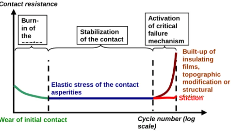
The second important point to be addressed is the reproducibility of the contact resistance over the actuations, and thus along its whole lifetime (cf. Fig. 2). The reliability of the switch depends on its ability to withstand some degradations occurring at the contact interface. Three types of phenomena can be studied: the mechanical (cold welding, strain hardening), electrical (arcing, hot welding, annealing) and chemical ones (formation of insulating films at the extreme surface), all inducing modifications of the topological, mechanical and electrical properties of the contact.
Figure 1. Typical lifetime of micro switches leading to contact
failure
As the experimental set-up developed here can be used to vary several parameters, the understanding of potential failure mechanisms can be made easier if the effort is put upon the identification of the key parameters for each mechanism. Moreover, these phenomena should be well described to explain any discrepancy between experimental measurements and the predicted values by the available models.
In addition, the contact temperature (Tc) of contact a-spots could be linked with the contact force depending on the contact voltage [5]. Indeed the plastic deformation of the asperities during the contact formation proceeds more rapidly when the softening temperature is reached [2]. Thus the effective contact area increases inducing a drop of the contact resistance. However the softening of the metal at the asperities of contact reduces the strain hardening of the a-spots and could accelerate the aging of the contact by the activation of thermal failure mechanisms. Therefore the softening temperature of contact metals is probably one of the most important critical parameter for a stable and low contact resistance.
EXPERIMENTAL METHODS
Description of the experimental set-up
The test described in this paper is based on methods combining a nanoindenter and a high resolution source meter for the determination of the electrical contact resistance versus the contact force and the displacement of the free standing part of the contact. The actuation load is thus reproducible and known with a good accuracy (10-9N and 10-10m), two points which remain hard to achieve with the actual actuations (for example, electrostatic actuation forces often drift due to dielectric charging).
Figure 2. Picture of the scan performed with the nanoindenter on
the test structure
Wear of initial contact
Elastic stress of the contact asperities Stiction Stabilization of the contact Burn-in of the contac Activation of critical failure mechanism Contact resistance
Cycle number (log scale) Built-up of insulating films, topographic modification or structural fatigue
The nanoindenter’s spherical tip is used as a mechanical actuator and can be applied on the sample with a 20nm accuracy positioning thanks to a piezo-actuated XY table. Thus a pseudo-AFM scan is performed by probing the surface with a fixed stiffness of contact between the tip and the surface (cf. Fig. 3).
The 4-wires electrical measurements are coupled with the nanoindenter software in order to control the level of load and the displacement of the tip by taking into account variations of the electrical resistance of the contact (cf. Fig 4).
Figure 3. Principle of the electrical test performed with a
nanoindentation tip
This experiment is also useful for studying hot switching or cold switching modes. In this way we are able to discriminate the failure mechanisms induced by the current or by the mechanical cycling of the contact. Moreover, the level of deformation sustained by the contact asperities (elastic, elasto-plastic or plastic) can be pointed out, depending on the applied load and actual contact area.
Test vehicle description
Specific test vehicles have been designed for contact analysis, enhancing the extraction of characteristic curves, and making possible the comparison between different contact shapes or materials. As illustrated in Fig. 5, the testing device is composed of a bridge suspended over the contact line. A 3µm square bump is processed underneath. The stiffness of the bridge is about 480 N/m. In addition, the test structures are designed to measure only the contact resistance as the resistance of the line is canceled by the 4-wire measurement process. The material contact is Au-to-Au because gold is the most popular material for electrical contact due to its high conductivity and its high resistance to oxidation.
Figure 4. Scheme of the test structures
T
ESTD
ESCRIPTION ANDR
ESULTSA campaign of tests has been made on these test vehicles to study the self heating of the contact with increasing level of current flowing through the contact. These performance tests enable us to compare the temperature of the contact with the analysis of the contact resistance versus the contact force up to 150 µN by sweeping the contact current from 1 mA to 100 mA and measuring the contact voltage in a cold-switching way. Moreover, the holding plateau at load max is fixed at 20s to study the creep of the contact. The load rate is about 1µN/s to allow the temperature to reach steady-state. The following results are based on the same 11 successive tests and are presented to emphasize the various observations allowing by this experimental set-up.
Sensitivity to current increase
0,5 1,5 2,5 3,5 4,5 5,5 6,5 0 20 40 60 80 100 120 140 160 Contact Force (µN) C o n ta c t re s is ta n c e ( ) I = 1mA I = 10mA I = 20mA I = 30mA I = 40mA I = 50mA I = 60mA I = 70mA I = 90mA I = 80mA I = 100mA
Figure 5. Contact resistance versus contact force as a function of
the current flowing through the contact
Fig. 6 shows typical contact force-contact resistance curves for a test structure with a 3µm square dimple at 11 levels of contact current. This curves point out the relationship between the contact force and normal load. The contact resistances decrease with the increasing contact force as a function of the contact current and are described by the equation x
C C AF
R = − where A and x are constant parameters. The parameter x decreases from 0.46 to 0.07 with contact current rising and does not fit with (2) because this equation does not take into account the roughness of the contact surface. The second observation is that the higher the current is, the lower is the dependence of the contact resistance to the load applied. The initial contact resistance remains
Bridge (Au) Fixed contact Bumps Top Side SiO2 x C AF R = −
4/5
lower for subsequent cycle at each increasing step of current.
The origin of this contact resistance reduction are thermally induced with the increase of the contact temperature with the current until reaching the softening temperature. Thus the annealing of the contact leading to a reduction of the contact hardness and the roughness of the contact is lower after softening of the surfaces. Thereby, the deformation of the contact asperities is higher with increasing current making easier the breakdown of insulating films, and enlarging the total contact area.
Contact temperature
Fig. 7 shows the contact temperature as a function of the contact current. The published softening temperature for gold contact is ~100°C, corresponding to a contact voltage of 70-80 mV for contact near room temperature [3]. We observe that when the contact current is increased after the first contact softening from 40 mA, the contact resistance continues to decrease keeping the contact temperature roughly constant. The contact temperature increases with constant slope from 1mA to 40mA. At this point the contact temperature stops to increase and fluctuates between 80°C and 120°C (65 mV to 75 mV). Thus when the softening temperature is reached, the contact temperature does not depends strongly on contact current at high current level.
Figure 6. Contact temperature versus the current flowing through
the contact asperities
Topological modification of the contact surface
As shown in Fig. 8, the number of asperities n, can be evaluated by the way of the mechanical measurements provided by the methodology. The stiffness of the structure can be measured by evaluating the load versus displacement slope and the occurrence of a new mechanical contact can be observed: A slight increase of this value is due to the deformation of the asperity of contact. When the contact force is high enough, new asperities come into contact, inducing a slight sudden modification of the loading configuration, that is to say a discontinuity in the stiffness recorded.
Figure 7. Evaluation of the number of asperities: number of steps
on the stiffness versus contact force as function of the contact current
We can observe that the effective contact area spreads with the number of the a-spots in contact while contact loads increase, while the contact resistance decreases. The total number of a-spots coming into contact also increases with higher contact current but the cross sectional area of a-spot also increases as they are pressed down. These two phenomena are in competition and it is hard to set apart one from each other. However we can conclude that the softening of the contact material leads to an increase of the number of contact a-spots.
A representation of the roughness of the contact bump in the test vehicle is obtained from AFM measurements (Fig. 9). The first picture shows the contact bump of a structure untested coming from the same run as the test used for the test campaign previously described. The second picture is the AFM imaging of the bump after the 11 successive tests (Fig. 6). We can observe the flattening of the asperities due to plastic deformation of the a-spots during the loading of the contact. The measurements point out that the rms roughness of the top of the contact bump decrease from 18.1 nm to 13.8 nm.
Figure 8. Roughness measurements performing by AFM with
non-tested bump (Ra = 18.1 nm and RMAX = 114 nm) (a) and tested bump
(Ra = 13.8 nm and RMAX = 90.0 nm) (b)
The ratio of the real contact area for each current level to the initial contact area for Ic = 1mA is evaluated from (1) and (2) at load max (Fig 10).
0 20 40 60 80 100 120 0 10 20 30 40 50 60 70 80 90 100 110 120 Current (mA) C o n ta c t te m p e ra tu re ( °C ) 0 1000 2000 3000 4000 5000 6000 7000 8000 0 10 20 30 40 50 60 70 80 90 100 110 120 130 140 150 Contact force (µN) S ti ffn e s s ( N /m ) n=7 n=8 n=5 n=3 I = 70mA I = 80mA I = 90mA I = 100mA a 2 µm b 2 µm 2 µm
Figure 9. Contact area ratio (A A0=R0² R²) versus contact
current
We observed that the contact area increases with a slope which is steeper from 50 mA. Indeed the inflexion point of 50 mA matchs with the rise of the contact temperature to the softening temperature. The plastic deformation is higher when the softening temperature is reached leading to a larger contact area in relation with a larger topographical modification of the contact surfaces.
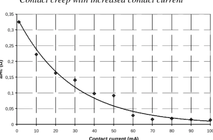
Contact creep with increased contact current
0 0,05 0,1 0,15 0,2 0,25 0,3 0,35 0 10 20 30 40 50 60 70 80 90 100
Contact current (mA)
R
c
(
)
Figure 10. Variation of the contact resistance during versus contact
current during the holding plateau at FC ~ 143 µN for t=20S
The variation of the contact resistance is recorded during the holding plateau for the 11 tests at load max (~143 µN) for each current level. The results are shown in the Fig. 11. The initial deformation is enough to support the load max applied on the contact and time dependant creep effects lead to additional asperity deformation during the holding plateau.
The variation of the contact resistance is directly linked to the contact area variation. We observed that the creep of the contact asperities is lower at high current although the contact material is softer. It could be explained by the fact that high current density in the asperities leads to a quick establishment of large contact area. Thus the larger contact area leads to a reduction of applied pressure on each a-spot and prevents to creep due to less stress at asperity contacts [1].
C
ONCLUSIONSThis new test facility had enabled to perform tests under realistic conditions in a static and dynamic way.
An emphasis was placed on the role of the current increase leading to contact heating in the understanding of the contact physics. Various phenomena were observed with asperity heating effects on contact resistance versus contact force dependence, stabilization of the contact temperature from the softening temperature of the contact material, modification of the surface topography, and diminution of the creep effect. All this mechanisms are commonly report as failure vectors in the contact switch lifetime.
And finally, this tests bring to light the usability of this methodology to investigate the contact reliability and performance under several test conditions. The test vehicles used in this study could be manufactured with several contact materials with various bump designs. The investigation on these two conception parameters governing the robustness of the contact and the contact geometry, which has a strong influence on the heat distribution across the contact, is underway. The knowledge gained will be the identification of the failure mechanism for each contact design in order to bring recommendations for further improvements of the contact reliability.
ACKNOWLEDGMENT
This work was supported by the ANR (Agence Nationale de la Recherche) in the frame of the FAME project. The authors would also like to thanks the CEA-LETI for the manufacturing of the test vehicles.
REFERENCES
[1] S. T. Patton, “Fundamental studies of Au contacts in MEMS
RF switches,” in Tribology Latters, VOL. 18, pp 215-230, 2005.
[2] A. Fortini et al., “Asperity contacts at the nanoscale:
comparaison of Ru and Au,” in arXiv:0807., New York, 2008.
[3] B. D. Jensen et al., “Effect of nanoscale heating on electrical
transport in RF MEMS switch contacts,” in Journal of
microelectromechanical systems, VOL. 14, NO. 5, pp. 935-946,
2005.
[4] R. Holm, “Electrical Contacts-Theory and Applications,” 4th ed.
Berlin Germany: Springer-Verlag, 1967.
[5] Hyouk Kwon and al., “Investigation of the electrical contact
behaviors in Au-to-Au thin-film contacts for RF MEMS switches,” in J. Micromech. Microeng. VOL., pp. 9, 2008.
[6] L. Féchant, “Le contact électrique,” Paris : Hermès, 1996.
0 2 4 6 8 10 12 14 16 0 10 20 30 40 50 60 70 80 90 100 Current (mA) A /A 0