HAL Id: tel-01267650
https://hal.archives-ouvertes.fr/tel-01267650
Submitted on 5 Feb 2016HAL is a multi-disciplinary open access
archive for the deposit and dissemination of sci-entific research documents, whether they are pub-lished or not. The documents may come from teaching and research institutions in France or abroad, or from public or private research centers.
L’archive ouverte pluridisciplinaire HAL, est destinée au dépôt et à la diffusion de documents scientifiques de niveau recherche, publiés ou non, émanant des établissements d’enseignement et de recherche français ou étrangers, des laboratoires publics ou privés.
integration of Ti(Al)N and Ta(Al)N for sub-20 nm metal
gate
Fabien Piallat
To cite this version:
Fabien Piallat. Plasma assisted chemical deposi-tion (CVD/ALD) and integration of Ti(Al)N and Ta(Al)N for sub-20 nm metal gate. Micro and nanotechnologies/Microelectronics. Université de Grenoble, 2014. English. �tel-01267650�
In order to get the grade of
DOCTOR OF GRENOBLE UNIVERSITY
Speciality: Micro and Nano Electronics
Ministerial order: 7 Ao ˆut 2006
Presented by
Mr Fabien Piallat
Thesis directed byMr Christophe Vall ´ee
and co-directed byMr Remy Gassilloud and Mr Pierre Caubet
prepared at Laboratoire d’Electronique et des Technologies de l’Information (LETI) du CEA Grenoble
in theEcole Doctorale Electronique, Electrotechnique, Automatisme & Traitement du Signal
Plasma assisted chemical
deposi-tion (CVD/ALD) and integradeposi-tion of
Ti(Al)N and Ta(Al)N for sub-20 nm
metal gate
Thesis publicly defended the4thof June 2014,
in front of the jury composed by:
Mme Blanquet Elisabeth
SIMAP, St Martin d’H `eres, Examinator
Mr Thomas Olivier
IM2NP, Marseille, Examinator
Mme Granier Agn `es
IMN, Nantes, Reporter
Mr Brice Gautier
INL, Lyon, Reporter
Mr Christophe Vall ´ee
CNRS-LTM, Grenoble, Thesis Director
Mr Remy Gassilloud
CEA-Leti Minatec, Grenoble, Thesis Supervisor
Mr Pierre Caubet
Je tiens `a remercier humblement tous ceux et toutes celles qui de pr`es ou de loin, m’ont permis de mener `a bien cette ´etude. Je suis intimement persuad´e qu’ils se reconnaˆıtront sans qu’il soit n´ecessaire de se livrer au traditionnel exercice de style que sont ”les remer-ciements”...
Contents
Acknowledgements iii
Abbreviations xi
1 MOSFET transistors: technological challenges 1
1.1 Microelectronic and improvements . . . 1
1.1.1 MOSFET: fundamental device in the CMOS technology . . . 3
1.1.2 Improved performance via scaling . . . 4
1.1.3 Improved performance via electrode tuning . . . 6
1.1.4 Improved performance via architecture . . . 7
1.2 Material integration for device fabrication . . . 9
1.3 Outline . . . 10
2 Deposition and characterisation tools 13 2.1 Introduction . . . 13
2.2 Deposition tools . . . 13
2.2.1 Precursors for CVD and ALD . . . 14
2.2.2 (Plasma Enhanced) Metal-Organic Chemical Vapour Deposition . . . 19
2.2.2.1 MOCVD principle . . . 19
2.2.2.2 Plasma for MOCVD enhancement or densification . . . 21
2.2.2.3 MOCVDs tool description . . . 23
2.2.2.4 Advantages, limitations and constraints . . . 24
2.2.3 (Plasma Enhanced) Atomic Layer Deposition . . . 25
2.2.3.1 Principle . . . 25
2.2.3.2 Tool description . . . 26
2.2.3.3 Advantages, limitations and constraints . . . 27
2.2.4 Physical Vapour Deposition . . . 28
2.2.4.1 Principle . . . 28
2.2.4.2 Advantages, limitations and constraints . . . 28
2.3 Characterization tools . . . 29
2.3.1 Four points probe . . . 29
2.3.1.1 Technique description . . . 29
2.3.1.2 Advantages, limitations and constraints . . . 30
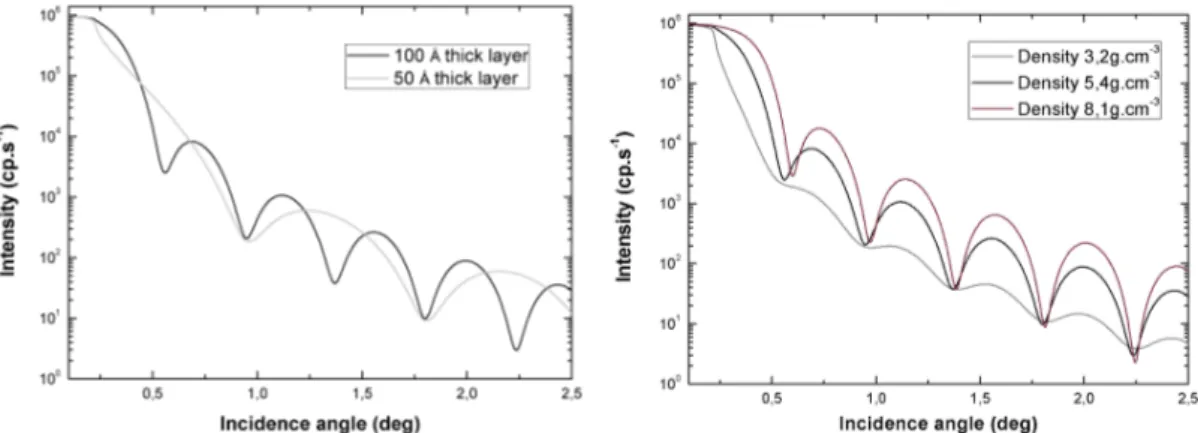
2.3.2 X-Ray Reflectivity . . . 31
2.3.2.1 Technique description . . . 31
2.3.3 X-Ray Diffraction . . . 32
2.3.3.1 Technique description . . . 32
2.3.3.2 Advantages, limitations and constraints . . . 33
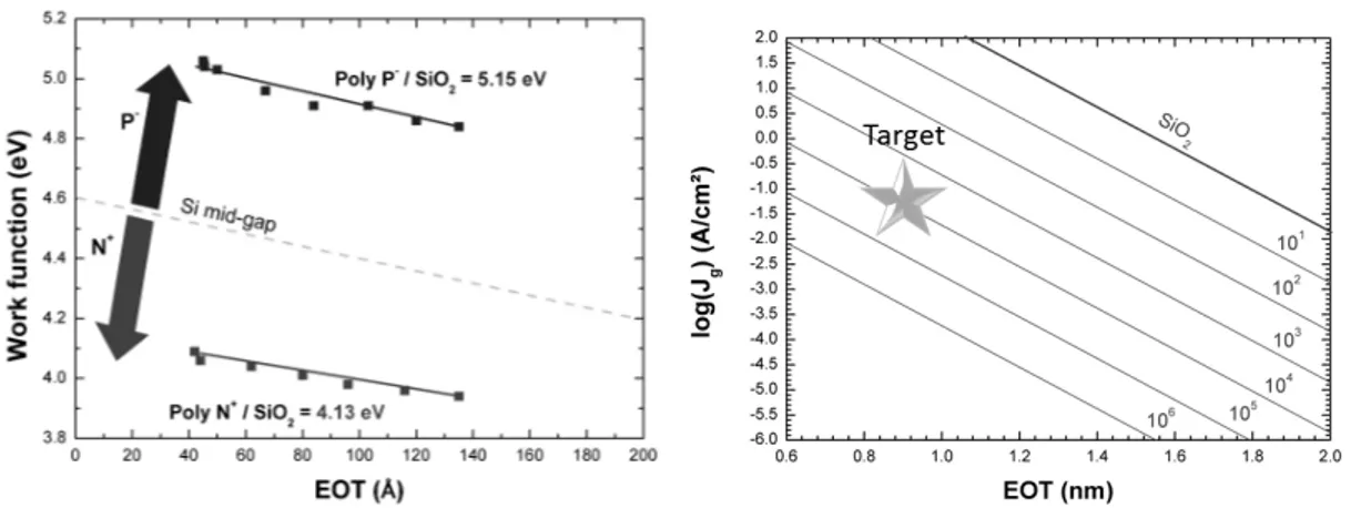
2.3.4 Secondary and Transmission Electron Microscopy . . . 34
2.3.4.1 Technique description . . . 34
2.3.4.2 Advantages, limitations and constraints . . . 35
2.3.5 Electrical measurements . . . 36
2.3.5.1 Technique description . . . 36
2.3.5.2 Advantages, limitations and constraints . . . 36
2.3.6 X-Ray Photoelectron Spectroscopy . . . 37
2.3.6.1 Principle . . . 37
2.3.6.2 Quantitative analysis . . . 40
2.3.6.3 Qualitative analysis . . . 41
2.3.6.4 Angle Resolved XPS (AR-XPS) . . . 42
2.3.6.5 Advantages, limitations and constraints . . . 42
3 Process influence 45 3.1 Introduction . . . 45
3.2 TaN MOCVD process parameters evaluation . . . 46
3.2.1 Context . . . 46
3.2.2 Methodology . . . 46
3.2.3 Substrate temperature . . . 47
3.2.3.1 Deposition with NH3 reactant gas . . . 47
3.2.3.2 Deposition with H2 and NH3/H2 mixed reactant gas . . . 50
3.2.4 Liquid injector temperature . . . 52
3.2.4.1 Methodology . . . 53
3.2.4.2 Deposited thickness and resistivity modification . . . 53
3.2.4.3 Chemical bonding evolution . . . 54
3.2.5 Deposition kinetics . . . 56
3.2.6 Effect of the injection frequency . . . 58
3.2.7 Discussion about TaN deposition reaction path . . . 59
3.2.7.1 TBTDET with NH3 reactant gas . . . 59
3.2.7.2 TBTDET with H2 reactant gas . . . 60
3.2.8 Conclusion . . . 63
3.3 TiN MOCVD process parameters evaluation . . . 63
3.3.1 Substrate temperature . . . 63
3.3.2 Deposition kinetic . . . 64
3.3.3 Discussion about TiN deposition reaction path . . . 65
3.4 Parameters influencing the uniformity . . . 65
3.4.1 Injection frequency . . . 65
3.4.2 Distance shower to substrate . . . 66
3.4.3 Vector gas flow . . . 67
3.4.4 Deposition chamber pressure . . . 69
3.5 MOCVD conformity control . . . 70
3.5.1 Methodology . . . 70
3.5.2 SEM conformity observation . . . 70
3.5.3 Roughness observation . . . 71
3.6 Conclusion to the Chapter 3 . . . 71
4 Plasma influence 73 4.1 Introduction . . . 73
4.2 Influence of plasma in PEMOCVD . . . 74
4.2.1 PEMOCVD standard parameters . . . 74
4.2.2 PEMOCVD plasma power variation . . . 76
4.2.3 Conclusion on PEMOCVD . . . 78
4.3 Influence of LF plasma power addition for PEMOCVD . . . 79
4.3.1 Introduction . . . 79
4.3.2 Experiments . . . 81
4.3.3 Plasma modification . . . 81
4.3.3.1 Impact of LF addition on pure Ar plasma . . . 82
4.3.3.2 Impact of LF addition on Ar+H2 plasma . . . 84
4.3.3.3 Modification of OES for Ar+H2+Ti precursor . . . 86
4.3.4 Thin TiN film analysis . . . 89
4.3.4.1 Impact of RF power on thin film properties . . . 89
4.3.4.2 Impact of LF addition to RF plasma on thin film properties 90 4.3.4.3 Impact of LF addition to RF plasma reaction mechanism . . 91
4.3.5 Conclusion . . . 94
4.4 Influence of plasma power in PEALD . . . 94
4.4.1 Introduction . . . 94
4.4.2 Experimental methods . . . 95
4.4.2.1 Samples preparation . . . 95
4.4.2.2 Characterisations . . . 97
4.4.3 Results . . . 97
4.4.3.1 Thickness and density . . . 97
4.4.3.2 Crystallography . . . 99 4.4.3.3 Chemical environments . . . 100 4.4.4 Discussion . . . 102 4.4.4.1 Composition . . . 102 4.4.4.2 Film density . . . 102 4.4.4.3 Film formation . . . 103 4.4.5 Conclusion . . . 104
4.5 PEMOCVD conformity control . . . 105
4.6 Conclusion to the Chapter 4 . . . 106
5 Interactions with sub-layer during metal integration 109 5.1 Introduction . . . 109
5.2 Impact of plasma on dielectric under-layer . . . 110
5.2.1 Context . . . 110 5.2.2 Experimental methods . . . 111 5.2.3 Results . . . 112 5.2.3.1 Chemical interactions . . . 112 5.2.3.2 Composition profile . . . 114 5.2.3.3 Electrical results . . . 115 5.2.4 Discussion . . . 116
5.2.4.2 EOT variation . . . 117
5.2.4.3 Leakage current evolution . . . 118
5.2.4.4 Φm(eff ) modification . . . 119
5.2.5 Conclusion . . . 119
5.3 Using TaCN reactivity for PVD-TiN electrical properties improvement . . . . 120
5.3.1 Context . . . 120
5.3.2 Experimental methods . . . 121
5.3.3 TiN and TaCN interactions analysis . . . 122
5.3.4 (PE)ALD-TaCN steps influence on PVD-TiN oxidation . . . 126
5.3.5 TiN layer modifications and oxide removal reaction mechanism . . . . 128
5.3.6 Particular impact of ALD and PEALD activation steps . . . 129
5.3.7 Correlation with electrical results . . . 130
5.3.7.1 Role of TiN layer in the stack . . . 130
5.3.8 Conclusion . . . 131
5.4 Conclusion to the Chapter 5 . . . 131
6 Aluminium doping 133 6.1 Introduction . . . 133
6.2 Aluminium doping in Physical Vapour Deposition . . . 134
6.2.1 Context . . . 134
6.2.2 Physico-chemical characteristics of Al-doped PVD-Ta and PVD-TaN . 134 6.2.2.1 Deposition conditions . . . 134
6.2.2.2 Characterisation of PVD-TaAl layers . . . 135
6.2.2.3 Characterisation of PVD-TaAlN layers . . . 139
6.2.2.4 Discussion on Ta and TaN materials doping with Al . . . 142
6.2.3 Electrical results from Al doping of PVD Ta and TaN . . . 144
6.2.4 Conclusion to PVD-Ta and PVD-TaN doping . . . 145
6.3 Aluminium deposition by (PE)MOCVD . . . 145
6.3.1 Context . . . 145
6.3.2 Experimental methods . . . 146
6.3.3 Thermal decomposition of TMA with NH3 . . . 147
6.3.4 H2 plasma decomposition of TMA . . . 149
6.3.5 Interpretation of MOCVD-AlN and PEMOCVD-AlC deposition . . . 150
6.3.6 Conclusion . . . 152
6.4 Al doping of MOCVD-TaN . . . 152
6.4.1 MOCVD-TaN doping characterisation . . . 153
6.4.1.1 Doping of TaN metal . . . 153
6.4.1.2 Chemical environments of MOCVD-TaAlN . . . 153
6.4.1.3 Localisation of Al in the layer . . . 155
6.4.2 Conclusion . . . 156
6.5 TaN and AlC multistacks formation by cycled (PE)MOCVD . . . 157
6.5.1 Context . . . 157
6.5.2 Tools and methods . . . 157
6.5.3 Characterisation of TaAlN multistacks . . . 157
6.5.3.1 Evolution of chemical bonding depending on the process . . 158
6.5.3.2 Crystallography . . . 160
6.5.4 Electrical characteristics of Al doped metals . . . 160
6.5.4.2 Evolution of the work function of MOCVD deposited TaAlN 161 6.5.5 Conclusion and perspectives . . . 162 6.6 Conclusion to the Chapter 6 . . . 163
7 Conclusions 165
7.1 Summary of the context . . . 165 7.2 Contributions . . . 166 7.3 Recommendations for future research . . . 167
A Comparison of Gate-First and Gate-Last flows 171
B List of metals successfully deposited by CVD and ALD 175
C Principle of X-Ray generation 177
Bibliography 181
Abbreviations
ALD Atomic Layer Deposition
AR-XPS Angle Resolved - XPS
a.u. arbritary unit
C-V Capacity - Voltage
CCP Capacitively Coupled Plasma
CVD Chemical Vapor Deposition
DF Dual Frequency Plasma
EOT Equivalent Oxide Thickness
FWHM Full Width at Half Maximum
HKMG High-κ Metal Gate
LF Low Frequency Plasma
I-V Current - Voltage
IC Integrated Circuit
ITRS International Technology Roadmap for Semiconductors
MOCVD Metal Organic CVD
OES Optical Emission Spectroscopy
PEALD Plasma Enhanced ALD
PEMOCVD Plasma Enhanced MOCVD
R2 Square Resistivity
RF Radio Frequency Plasma
sccm standard cubic centimeter per minute SEM Scanning Electron Microscopy
Ta(C)N Tantalum(Carbo)Nitride
TBTDET Tertiary-ButylimidoTris(DiEthylamino)Tantalum TDEAT Tetrakis(DiEthylAmido)Titanium
TEM Transmission Electron Microscopy Ti(C)N Titanium(Carbo)Nitride
TMA TriMethylAluminium
UHV Ultra High Vacuum
XPS X-Ray Photoelectron Spectroscopy
XRD X - Ray Diffraction
MOSFET transistors: technological
challenges
“We’re so accustomed to the marvels of everyday thought that we never wonder about it.” Marvin Minsky, scientist
1.1
Microelectronic and improvements
Over the past few decades, semiconductor industry has witnessed dramatic rise in the per-formance of integrated circuits and in the subsequent financial market growth. Perper-formance improvement at lower cost in microelectronic integrated circuits (ICs) has been achieved by increasing transistor speed, reducing transistor size and packing more transistors onto a single chip.
This trend was first foreseen by Intel co-founder Gordon Moore, who, in his article in the year 1965 observed that the number of components in integrated circuits has doubled every year from the invention of the integrated circuit in 1958, by Jack Kilby (Nobel prize in 2000) [1], until 1965. G. Moore predicted that this trend would continue ”for at least ten years” [2]. From the beginning of mass production, the number of transistors that the industry was able to place on a computer chip did double every two years (figure 1.1) [3]. This prediction, now known as the Moore’s law, is responsible for the evolution of today’s complementary metal-oxide-semiconductor (CMOS) technology. Recognition of this observation has proven to be accurate, in part because the law is now used in the semiconductor industry to guide long-term planning and to set targets for research and development, resulting in the auto-fulfilling of the hypothesis made by G. Moore. Thus, the transistor has shrunk from the size of a pencil eraser to smaller than a bacterium for the latest generation.
Transistor has become the workhorse component of almost every electronic device after it was invented by John Bardeen, Walter Brattain and independently by William Schokley at the Bell Laboratories in 1947. They shared a Nobel Prize in 1956 for their classic discovery of point-contact transistors and bipolar transistors [4].
The salient feature of transistors which fuels the rapid growth of the information technology industry is the incredible increase in their speed and drop in cost per component as their
Figure 1.1: Evolution of the number of transistors placed on a chip
size is reduced.
In simple terms, a transistor can be described as a three terminal semiconductor device in which the input signal controls the output current and which performs the functions of switching and amplifying. Use of transistor is extended in areas like amplifying low frequency radio signals, analog to digital signal transformation and vice versa, high speed computers, etc. Increase in the processor performance results not only from increase in the transistor density but also from the improvement in the transistor functionality. Transistor can be improved both through materials and architecture changes. Based on design and operating behaviour, transistors are classified into two major types: bipolar junction transistor and Field-Effect Transistor (FET) [5], presented in figure 1.2 left and right respectively.
In the 1960s, the IC market was broadly based on bipolar transistors due to their high switching speed and low power consumption at smaller sizes. But since 1975, integration of FETs prevailed even though they were found to be slower switching devices than the bipolar transistors [6]. This was caused by the failure of bipolar transistors to demonstrate rapid decrease in the power per circuit compared to FETs. As linear dimensions reached the half-micron level in the early 1990s, the performance advantage of bipolar transistor was outweighed by FET (more specifically MOSFET, a modern and more practical variant of FET), then used in the CMOS circuit production till today.
Figure 1.2: Bipolar (left) and MOSFET (right) transistors schemas
The choice of FET over bipolar was also comforted by:
a. the ease of scaling. Whereas the drain current of bipolar devices has an exponential dependence on base-emitter voltage, the MOSFET drain current depends on the ratio of its geometry (width/length). Thus, the MOSFET characteristics remain the same as far as the W/L is kept same; necessarily leading to easier scaling down of the device. b. the lower power. CMOS logic consumes less power compared to bipolar. This is due to the fact that complementary logic in MOS gives zero static power dissipation, which is not the case for bipolar junction.
c. the ease of production. MOSFET fabrication is easier because bipolar junction requires complex processes which includes buried layer.
Improvements can be applied to different aspects of the devices for ever competitive devices. First one coming into mind is the scaling, i.e. the size reduction of the structures. Then architecture is adapted to the new thickness before the development of new materials. These three points are investigated in next sections of this chapter.
1.1.1 MOSFET: fundamental device in the CMOS technology
Metal-oxide-semiconductor FET (MOSFET) is essentially a metal-insulator-semiconductor junction provided with a source and a drain, as shown in figure 1.2. In a MOSFET structure, a dielectric material (mainly silicon dioxide, SiO2) is used as the insulation layer, called a
gate oxide, which is placed between the gate electrode and the semiconductor, called chan-nel, made of silicon in the crystalline state. The diagram, in figure 1.3, makes easier the understanding of MOSFET operating, assuming that the substrate is a p-type semiconduc-tor which has positively charged mobile holes as carriers, and that the source and drain are made of doped n-type (denoted by n+) material, as presented in figure 1.3a. When a
positive voltage is applied on the gate (Vg), figure 1.3b, an electric field causes the holes to
be repelled from the interface, creating a depletion region containing immobile negatively charged acceptor ions. A further increase in the gate voltage above the threshold voltage (Vth), figure 1.3c, eventually causes electrons to appear at the interface, in what is called
inversion layer (n-MOS).
Figure 1.3: CMOS working conditions schema, a: off conditions, b: depletion condition, c: inversion canal creation condition
FETs evolved from p-type MOSFETs (p-MOS) in the 1960s to n-type MOSFETs (n-MOS) in the 1970s and then to CMOS in the 1980s and 1990s. CMOS circuits combine both n-MOS and p-MOS in a way which greatly reduces consumption of power. Other architectures were proposed to replace CMOS but never made it to the production maturity.
1.1.2 Improved performance via scaling
’Scaling’ is a practice term invented to describe reduction in the size of the device dimensions in order to fit more components on a single microchip. Calculated reduction of transistor geometries as well as the capacitor cell area in the IC has demonstrated spectacular expansion in the technology and communication markets [7]. The prime elements which enable the scaling of the Si-based MOSFET are the materials properties associated with the dielectric employed to isolate the transistor gate from silicon channel.
Early CMOS devices mainly consisted of thermally grown amorphous silicon dioxide as the gate dielectric which is the smallest feature of the device. SiO2layer has a major influence on
the device electrical behaviour, it acts as a perfect insulator between the gate and the channel, thus preventing short circuits. As the transistor feature size is shrinking, the corresponding gate dielectric thickness is also decreasing rapidly. The problem associated with thinning of the oxide layer is its inability to store or to flow large amount of current in it, thus greater leakage current occurs through the dielectric layer. In an ideal situation, the gate dielectric acts as a perfect insulator, but as it is made ever thinner in order to improve the device performance, huge amounts of current leaks through it thereby resulting in higher power consumption, and turning the device cost ineffective. This problem became even more determining with the apparition of mobile devices which have limited power but need more and more calculation power.
At normal device operating condition, the typical leakage current of SiO2 at a gate bias of 1
Volt, changes from 10−12 A.cm−2 at 35 ˚A to 1 A.cm−2 at gate oxide thickness of 15 ˚A. To avoid high leakage currents and still achieve the required gate capacitance, a material with higher permittivity is needed.
capacitance (C):
C = εε0A
t (1.1)
where ε is the dielectric constant (also referred to as the relative permittivity) of the mate-rial, ε0 is the permittivity of free space (8.85x10⁻¹² F.m−1), A is the area of the capacitor
and t is the thickness of the dielectric. To keep similar behaviour of the devices, C has to be kept constant, so as mentioned earlier, parameter A will be growing only smaller in the future semiconductor technologies if no change is made to the architecture of the transistor. Thus to keep C constant with a decreasing A, t can be decreased or ε be increased. However, if t is reduced the leakage current will grow, and from equation 1.1 it is apparent that the dielectric layer thickness t can be increased in order to avoid high leakage currents, only when a material with higher relative permittivity ε is used. These materials with higher relative permittivity are called high-κ materials and represent one of the main parameters investigated for new technology nodes.
In order to compare the dielectric layer of different materials, the use of the equivalent oxide thickness (EOT or teq) parameter was introduced. The term teqcharacterises the theoretical
thickness of SiO2 that would provide a particular capacitance density assuming standard
dielectric constant of 3.9 (disregarding issues like leakage current and reliability). Therefore, equation 1.1 for capacitance can be rewritten in terms of teq and εox (3.9, the dielectric
constant of SiO2) of the capacitor as follows:
teq εox = thigh−κ εhigh−κ (1.2) or simply: teq= εSiO2 εhigh−κ thigh−κ= 3.9 εhigh−κ thigh−κ (1.3)
From equation 1.3, it appears that a gate oxide material having a dielectric constant of ∼ 25 affords to have a physical thickness of ∼ 64 ˚A to obtain teq of 10 ˚A.
In the real world some interactions happen between the dielectric and the substrate or metal. Thus the equation becomes:
EOT = teq= tSiO2 + X i 3.9 εi tdielectrici (1.4)
where tSiO2 is the physical thickness of the SiO2 interface layer, also referred to as IL,
tdielectrici is the physical thickness of the dielectric i, εi the dielectric constant of the film
and the summation over ”i” is for stacks that do not have an uniform profile or are made of several dielectrics.
To further reduce the EOT one could think that tSiO2 could be reduced or even removed
from the device. However, nucleation of the dielectric is favoured by the presence of SiO2
generally creation of silicon oxide at the silicon/dielectric interface. The removal of SiO2
also results in the degradation of mobility and reliability of the devices due to the direct contact of the high-κ with silicon. Still, if a Si wafer is cleaned before dielectric deposition, a natural oxidation of the wafer’s extreme surface happens when in contact with the air. This oxidation, about 5-6 ˚A may continue to grow during device manufacturing. Thus, in order to control this SiO2 IL and obtain a good quality oxide, with 3.9 dielectric constant and
avoid any regrowth, a chemical oxide is formed at the surface of the sample, with a thickness stabilised around 7-8 ˚A.
It appears that today, the continuous scaling of microelectronic devices has reached more or less its limits with the known materials. New materials are needed to meet the requirements of the coming technologies. As introduced, high-dielectric constant materials have already partially replaced silicon dioxide together with metal-gates replacing polycrystalline silicon.
1.1.3 Improved performance via electrode tuning
If EOT and current leakage are mainly controlled by the dielectric properties, threshold volt-age, work function and interfacial defects can be tuned by carefully choosing the material used for the electrode. For a long time, polycrystalline silicon was used for the creation of electrode due to the easiness of doping Si to obtain n-type or p-type material. In ultra-thin oxide systems, when EOT reaches less than 2 nm in thickness, the parasitic capacitance induced by poly gate depletion becomes a first order phenomenon. It leads to a capacitance in series with the gate oxide, which results in the increase of the EOT. One solution is to highly dope the polysilicon, but the ionised dopants and the parasitic charge density increase with increased doping. These parasitic gate charges act as charge centres in the gate and scatter the carriers in the channel thus degrading the device performance, an effect called Remote Coulomb Scattering (RCS). Since parasitic gate charge density should be decreased, a reduction of gate doping concentration is necessary. Thus, it is clear that the effects of polygate depletion and/or RCS are unavoidable in conventionally doped gate CMOS devices. To improve device performance, it appeared that the gate depletion must be completely elim-inated. Hence metal gate provides a solution to eliminate poly gate depletion effect. Also, to ease integration and avoid interactions from superior metal layers deposition or reaction, metals with good chemical barrier properties have to be chosen. The gate in CMOS devices is generally of the same type as that of the source/drain, i.e. the NMOSFET has a n-gate and PMOSFET has a p-gate.
Some of the most extensively studied and most promising materials are titanium and tan-talum alloys [11–13], in particular nitrides, thanks to their high thermal stability [14], low reactivity [15, 16], low electrical resistivity [11, 17, 18] and their wide range of work function [12, 14, 17, 19–21]. Moreover, creation of new alloys, based on these metals, can lead to the fine tuning of the work function. In particular, carbides or aluminium alloying can signifi-cantly shift the effective work function of the metal [22, 23].
Although much work has been done so far on the understanding of metals, more studies need to be conducted on the interactions taking place at the metal / dielectric interface. Moreover, materials deposited later on during the integration flow are equivalent to a low temperature annealing, and so can enhance the interactions and the damages created at the interface.
To ease the integration of new materials in the production chain, different architectures can be chosen to lower the process constraints.
1.1.4 Improved performance via architecture
If material tuning is one solution to allow a reduction of the devices size, changes in the architecture and flow is another. MOS transistors have been built, for many generations, using a gate-first approach. In this approach the metal forming the gate is deposited before the formation of the drain and source by implantation, and subsequent the high temperature anneal performed to activate the dopants in the Si substrate. This high temperature activa-tion anneal can strongly impact the integrity of the dielectric/metal stack. Even if data on the effect of process temperature on work function are clear [24, 25], the advantage of the already existing work flow has kept focus on gate first approaches. However, given the need to reduce gate dielectric current leakage, to reduce the metal gate depletion and considering the interactions taking place at the metal/dielectric interface, the benefits of a lower thermal budget are immediate and integration of the high-κ/metal gate stack into the transistor flow is mandatory for new technology nodes. Such approach is referred to as the replacement gate process or gate-last flow (in opposition to gate-first), which enables decoupling of the junction formation from the dielectric/metal gate formation step. In this flow, a sacrificial poly gate is used and then removed after the junctions formation. Consequently, the gate dielectric and the metal gate are deposited after the high temperature anneal. A comparison of unique steps in metal gate-first and gate-last process flows is given table 1.1, with the key differences highlighted in bold. Because of its low thermal budget, the gate-last integration flow opens new possibility to carefully tune the work function and to provide devices with the desired threshold voltages.
The gate-last architecture was first introduced in mass production by Intel in 2007 for the 45 nm technology node [26].
A more complete description and comparison of Gate-First and Gate-Last approaches is pre-sented Appendix A, page 171.
On top of these two approaches, a plethora of modifications to the gate first or gate last methodologies have been and continue to be discussed in the scientific literature.
Another way to improve the performance by architecture modification is the introduction of Silicon On Insulator (SOI) substrate. SOI substrates are layered silicon-insulator-silicon and
Table 1.1: Comparison of Gate-First and Gate-Last flows
Gate-First Gate-last
Isolation Isolation
High-κ gate deposition High-κ gate deposition Dual Metal-Gate deposition Sacrificial Poly-Silicon gate
deposition/patterning Poly-Silicon gate deposition
Poly-Silicon/metal etch Source/Drain formation Source/Drain formation Salicide/Contact etch stop Salicide/Contact etch stop Sacrificial Poly-Silicon gate
removal 1st Inter-Layer Dielectric
deposition/polish Dual Metal-Gate deposition
Contact formation Contact formation
replace the conventional silicon substrate: schematic description is given in figure 1.4. The benefits of SOI relative to conventional silicon includes: low parasitic capacitance due to the isolation from the bulk silicon, which improves power consumption at matched performance; and resistance to short-circuit due to complete isolation of the n- and p-well structures. SOI substrates can easily be integrated in the current technology without modifications of the process flow.
Figure 1.4: SOI schema
Introduction of 3D architecture, also called Tri-gate, in the last half-decade was investigated as a possible solution [27]. 3D transistors employ a single gate stacked on top of multiple vertical gates, as visible in figure 1.5, allowing to duplicate the surface area at which the electrons can travel. And as introduced in equation 1.1, increase of the transistor surface area allows to increase the gate capacitance. Reports showing that 3D transistors reduce leakage and consume far less power than current transistors have been made. This allows up to 37% higher speed, or a power consumption at under 50% of the previous type of planar transistor [28, 29]. Additional control over the gate enable as much transistor current flowing as possible when the transistor is in the ’on’ state (for performance), and as close to zero as possible when it is in the ’off’ state (to minimise power loss), and enable the transistor to switch very quickly between the two states (again, for performance).
Figure 1.5: Planar and 3D transistors schema
This architecture has opened new opportunities but new difficulties also rose with it. One of the most challenging difficulty is the need of conformal and uniform deposition on all the surfaces of the structures with a layer as thin as one nanometre [30]. Conformal deposition leads to the need of a non-directive, non-preferential method, thus to surface reactant depo-sitions. Depositions based on chemical principle are hence preferred to the physical one, with a particular interest for metal-organic chemical vapour deposition to keep the cost down and to be easily industrialised.
Once the material matching the aimed physical characteristics is obtained and the archi-tecture of the device is known, some work has to be done on the integration. Interactions between the various materials of the device can lead to unwanted and negative effects, result-ing in the degradation of the electrical properties. To limit these interactions, lowly reactresult-ing materials but also soft processes have to be chosen for device fabrication.
1.2
Material integration for device fabrication
As explained in the previous paragraphs, a transistor, which is the basic component of any device, can be described as a precise superposition of materials, which are controlled at the atomic level, which are deposited as thin films on a semiconductor substrate and which are interacting between each other. Due to the ever-decreasing size of ICs, interactions between the materials are becoming more and more important and they now define the general be-haviour of the devices. Therefore, thin film deposition has evolved to become a stringent, meticulous field within surface science: deposited films in ICs require sub-nanometre di-mensions and extremely low levels of contamination (to avoid altering the properties of the deposited materials) [31–37].
Paradoxically, the solution for the first problem, the use of chemical deposition methods, has worsened the second.
Initially, deposition was mainly performed through evaporation or sputtering methods (known as physical vapour deposition PVD), where a source of pure material was vaporised, using electron beam, ion beam or plasma, and deposited on a substrate [38–40]. However, the direction-dependency of these methods led to some unsolvable problems with smaller size
devices. The use of volatile molecular compounds instead of solid sources allowed an ho-mogeneous growth of the layers, even on demanding aspect ratios. Originally, inorganic compounds were chosen (metal halides were the most used), but they required rather high temperatures and the byproducts were corrosive [40, 41]. Although these drawbacks were overcome with the use of metalorganic precursors, [41, 42] an inherent problem was the in-troduction of undesired elements (in particular carbon) into the growing film [40, 43]. Moreover, due to this choice toward Chemical Vapour Deposition (CVD), pure materials cannot be obtained anymore. Only alloys, such as oxides, nitrides or carbides, are deposited and require new developments for integration.
CVD is a surface reactant deposition, which implies that the deposited material is interacting with the under-layer. And because of thickness reduction of the layers the surface-volume ratio is reducing, leading to more and more significant surface interactions for the definition of the devices behaviour, compared to the previous generations of CMOS. These surface interactions compel the choice of lowly reactive materials and deposition methods, especially when plasma is introduced in the process. Concessions have to be done when choosing the best material with the lowest interactions.
This thesis took place in the described context and some of the previously mentioned chal-lenges and opportunities were investigated. Part of the results, from a three years long work, are presented in this thesis.
1.3
Outline
As introduced in the previous sections, alternative candidates for metal gate with suitable properties and limited interactions with dielectric, are needed for future generations of CMOS technology. To achieve this, new materials, or new processes to tune the characteristics of these metals, have to be investigated. Then, it is necessary to have a better understanding of the physico-chemical phenomenons taking place at interfaces during deposition. Moreover, a correlation has to be done between material changes and possible changes of the electrical behaviour of the complete devices.
MOCVD-deposited titanium and tantalum alloys are widely investigated as potential re-placement of the actual titanium nitride PVD metal gate, in order to fulfil the conformity demand. MOCVD allows conformal deposition, important for gate-last and FinFET inte-gration, but also results in nitride and/or carbide alloys and contamination, whose levels are important to control.
MOCVD is a general naming which includes several deposition methods, all based on the chemical reaction of metal-organic precursor with the substrate and a reactant gas. Thus, Atomic Layer Deposition (ALD), Liquid Injected MOCVD (LIMOCVD) and Plasma En-hanced LIMOCVD (PELIMOCVD) are part of the MOCVD group. A description of these
techniques is given in the Chapter 2, with an emphasis on the differences of reaction mech-anism paths.
To study the deposited metals in terms of physical and chemical properties several charac-terisations techniques are used. Hence, the physical characteristics of the layers, i.e. den-sity, thickness, roughness are obtained by X-Ray Reflection, resistivity and crystallography, by four points probes and X-Ray Diffraction measurements respectively. Composition and chemical interactions are investigated by means of X-ray Photoelectron Spectroscopy. These characterization techniques and the corresponding methodologies are described in Chapter 2.
In Chapter 3, influences of the deposition process on the deposited metal properties, during MOCVD and ALD are studied. Effects of the variation of substrate and injectors tempera-ture, reactant gas, pressure and other process parameters are discussed. These parameters are carefully tuned to achieve a full understanding of the changes in the properties of the deposited material. The characteristics closely looked at are the deposition rate, density, roughness, resistivity, composition and bonding environment of the species. Depending on the variation of the previously mentioned characteristics deposition reaction mechanisms are discussed and linked to the deposition parameters.
Similar methodology is used in the Chapter 4, for an investigation of the plasma in PE-MOCVD or PEALD modes. The influence of each of the plasma parameters on the de-position reaction path is studied. Then, the addition of low frequency plasma for better decomposition of the precursor in PEMOCVD is reviewed in details. Using optical emission spectroscopy the modifications of the plasma are correlated to the modifications of the de-posited material. In the last part of this chapter plasma is introduced for densification of Ta(C)N, in a PEALD mode. Evolution of the physical properties are linked to the chemical evolution of Ta(C)N when the plasma power is increased.
Then, because there is a thickness reduction of the deposited materials, the volume/surface ratio is also reducing and it gives an ever rising importance to surface reactions. Indeed, at thicknesses of two nanometres and below, more than half of the atoms composing a layer are in contact with bottom or top materials. An investigation of these interactions happening at the metal-dielectric interface is presented in Chapter 5.
By carefully choosing the deposition process it is also possible to promote some interactions, such as oxide removal or nitrogen addition, resulting in the improvement of the stack proper-ties. MOCVD deposition reaction mechanisms are based on chemical affinity of the precursor with the reactant gas and with the substrate, thereby reactions with the underlayer cannot be avoided. Illustration of the point will be done by a study of the Ta(C)N interaction with TiN in Chapter 5.
Reciprocity is valid, the substrate have an influence on the nucleation of a new material.
Finally, in Chapter 6 the first results concerning Al doping of TaN deposited by PVD and MOCVD are compared. Complete investigation of PVD-TaAl and PVD-TaAlN highlighted the important role of Al for passivation of the film, thus limiting the oxygen diffusion in
the volume of the layer. Successful deposition of MOCVD-AlN and PEMOCVD-AlC is used to acquire some knowledge about MOCVD doping, and used as reference for comparison with MOCVD-TaAlN deposition. ARXPS analysis of MOCVD-TaAlN layer confirmed the Al2O3 passivation layer formation, supposed from the study of PVD-TaAl and PVD-TaAlN.
Then, to limit the creation of AlN, observed at the deposition of MOCVD-TaAlN, multistack materials containing Al-Al and AlC are developped and compared to MOCVD-TaN. The electrical results are discussed in relation to the physico-chemical characterisations and to Al doping behaviour in PVD-Ta.
Deposition and characterisation
tools
“Do not wait; the time will never be just right. Start where you stand, and work with whatever tools you may have at your command, and better tools will be found as you go along.” Napoleon Hill, author
2.1
Introduction
Since the introduction of IC to mass production, in the late 1960s, new deposition methods have been developed to answer the specific needs of this demanding industry. At the same time, to understand the phenomenons taking place during the deposition, improvement of the characterisation tools was achieved.
Today this pair, deposition/characterization, allows to create, control and characterise layers at the atomic level. A new world of possibilities and understanding is now at reach. This change was confirmed by the evolution of the number of publications concerning surface and interface studies. Indeed, in the last forty years it rocketed up from less than 100 up to almost 3000 (figure 2.1).
In this chapter are presented the tools used for deposition and characterization of the in-vestigated metals and of the interactions with the substrate taking place during deposition. For each tool the physico-chemical principle is described and a discussion is given on the advantages, limitations and constraints consecutive to the metal-gate thematic. Emphasis is laid on Metal Organic Chemical Vapour Deposition and X-Ray Photoelectron Spectroscopy, the most used deposition and characterization methods of this work.
2.2
Deposition tools
The tools used for deposition during this thesis were industrial or pre-industrial modules, it implies that the recipes are already provided by the manufacturer in the industrial module,
Figure 2.1: Evolution of the number of publications in surface and interface science referenced in ScienceDirect database
whereas no process is included with pre-industrial module. A direct consequence is that modifications of the process, to extreme conditions, are much easier with the pre-industrial module. However, reaction mechanism used in industrial modules have to noticeable advan-tage of being stable, reproducible and already investigated in details.
2.2.1 Precursors for CVD and ALD
CVD and ALD are based on chemical reactions; every reaction needs reactants to obtain the products. In the case of metal deposition the reactants consist of the metallic atoms in solution, called a precursor, and a reactive gas. As introduced Chapter 1 section 1.2, the best metal compounds for metal gate application are the metalorganic precursors.
Metalorganic precursor is defined as a chemical compound that contain metal and organic ligands. Metalorganic compounds exclude species with direct metal-carbon bonds, which are classified as organometalic compounds.
Metalorganic precursors have several advantages for film growth compared to the elemen-tal sources that are used in physical vapour deposition processes and to the meelemen-tal halides that are often used in CVD processes. Most importantly, metalorganic precursors tend to be much more volatile than many metal halides and most metals in their elemental form, which allows easy precursor delivery systems. Since film growth occurs by a succession of chemical reactions, the precursor chemistry can be designed to favour the desired inorganic phase, minimise undesirable element incorporation into the final material, control the depo-sition temperature and avoid corrosive by-products that might damage the reactor or the substrate on which the film is grown. Metalorganic precursors can also be obtained in high chemical purity, which is important for microelectronic application. Indeed ultra pure met-alorganics are required, with purity of the order of 99.9999% or greater.
Many different types of ligands have been employed to create volatile metalorganic precur-sors for film growth. In general, the ligands are anionic, with carbon, oxygen or nitrogen donor atoms. In some cases, neutral donor ligands are present. Many CVD processes entail the reaction between a metalorganic precursor with basic ligands and a co-reactant that contains acidic element-hydrogen bonds. Mixing of these reactants in the gas phase results in protonation1 reactions that eliminate the basic ligand in its protonated form and in the formation of a new metal-element bond (equation 2.1) [35, 42, 44].
M − R + EHn
CV D reactor
−−−−−−−−→
−RH M − EHn−1 (2.1)
with M the metal atom or heteroatom, E the reactant atom such as O, N, S.
The co-reactant with acidic element-hydrogen bonds is generally chosen so that the element corresponds to one of the atoms required for the final film material. Examples of this type of reactant include ammonia and water for the deposition of nitrides and oxides, respectively. A second type of strategy that is used to eliminate excess hydrocarbon groups from the metalorganic precursor is β-hydrogen elimination [45, 46]. Hydrocarbon groups such as Et,
nPr, iPr, nBu and iBu, when bonded to a metal atom or a heteroatom, can eliminate an
alkene through a low-energy decomposition pathway [46, 47]. This β-hydrogen elimination often provides an efficient pathway through which carbon groups are removed from precur-sors. If a precursor is properly designed, the carbon incorporation in the film material can be minimised.
Deposition by MOCVD and ALD was reported for many elements of the periodic table, a list of these elements and the deposited materials is presented Appendix B, page B.
MOCVD and ALD appear as a viable solution for microelectronic but critically rely upon the availability of suitable high-purity precursors with sufficient volatility and stability. Ar-ticles, books and reviews addressing this subject have been widely published in the past few years. The role of molecular chemistry in influencing the physical properties of the precursor leading to robust thin films has been widely discussed [35, 36, 44–48]. To be compatible with microelectronic applications the precursor must possess the following properties:
• Appreciable volatility and molecular stability of the vapours to avoid pre-gas phase reactions or decomposition of the vapours, and to achieve film growth at moderate deposition temperatures.
• Adequate temperature window between precursor evaporation and decomposition to get high quality deposits preferably at lower substrate temperatures.
• Clean fragmentation of the organic matter at the surface of the substrate during film growth, to limit the by-products contamination.
• Easily synthesised and purified in high yields at reduced cost, convenient during han-dling and transportation, preferably a low degree of toxicity to easier the maintenance
of the deposition tool.
Of course, such a precursor do not exist and compromises have to be done. Vapour pres-sure of a metalorganic precursor is the crucial parameter that governs the concentrations of metalorganic precursors entering the reactor, and subsequently the growth rate of deposition process. Also low vapour pressure allows to limit the necessary temperature of the system, including the capillary tubes from the canister to the deposition chamber.
Thus choosing a precursor is not an easy task and should not be underestimated.
One precursor of both tantalum and titanium were chosen to match the deposition constraints of the metal for high-κ/metal gate deposition application, the properties of the metal and the aimed process window.
Tantalum precursor:
Several precursors are commercially available for Tantalum nitride deposition. Most used for CVD and ALD processes are the TertiaryButylimido,Tris(DiEthylamino)Tantalum (TBT-DET), t-Amylimidotris(dimethylamido)tantalum and Pentakis(DiMethylAmido)Tantalum (PDMAT) [18, 49–52].
Table 2.1: Comparison of TBTDET and PDMAT precursors
TBTDET PDMAT
Formula Ta(NtBu)(NEt2)3 Ta(NMe2)5
Molecular Weight 468.46 g.mol−1 401.33 g.mol−1 Boiling point 120◦C @ 1 Torr 100◦C @ 0.1 Torr Vapour pressure ∼ 1 Torr @ 120 ◦C ∼ 1 Torr @ 90 ◦C
Flash point 46 ◦C NA
Due to the different intrinsic properties, it was already proven that TBTDET is more suited for tantalum nitride metal deposition. When using PDMAT and NH3 it was reported that
films with some Ta and N could be grown, but that they contained a great deal of carbon and were non-conducting due to the formation of Ta3N5 phase (a nitrogen rich dielectric)
[53]. In contrast, when TBTDET was used with NH3 electrically conducting films of TaN
were created with low carbon content and low resistivity [18, 54, 55].
Thus, for MOCVD and ALD the TBTDET molecule was chosen. TBTDET molecule is presented in the diagram figure 2.2.
Two noticeable features of this molecule are: one the lack of tantalum-carbon bonds and second the presence of a double tantalum-nitride bond. These features dictate the stoichiom-etry of the deposited material.
Titanium precursor:
As for tantalum, few titanium metalorganic precursors are commercially available. Most used precursors for titanium nitride deposition are Tetrakis(DiEthylAmido)Titanium (TDEAT)
Figure 2.2: Skeletal formula of tantalum TBTDET precursor molecule
and Tetrakis(DiMethylAmido)Titanium (TDMAT) [17, 56–61].
Table 2.2: Comparison of TDEAT and TDMAT precursors
TDEAT TDMAT
Formula Ti(NEt2)4 Ti(NMe2)4
Molecular Weight 336.4 g.mol−1 224.19 g.mol−1 Boiling point 60◦C @ 1 Torr 65◦C @ 1 Torr Vapour pressure 1 Torr @ 100 ◦C 0.0067 Torr @ 25 ◦C
Flash point 10 ◦C NA
Previous investigations showed that, even if TDEAT has a higher temperature process win-dow it is more suited for TiN MOCVD and ALD deposition [59]. Advantages over TDMAT include: better decomposition of the precursor molecule and lower resistivity obtained at the same substrate temperature.
Hence, if the process temperature can be above 250◦C then TDEAT precursor is a better choice. Because metal for the gate can be deposited at temperatures up to 400◦C without any damageable consequences on the substrate, TDEAT was chosen.
TDEAT molecule is presented in the diagram figure 2.3.
As for tantalum molecule, titanium precursor do not present any carbide bonds, the metal atoms are only bonded with nitrogen atoms.
Finally, to do the doping of tantalum and titanium nitride layers, aluminium was chosen. Aluminium doping was already widely studied in the case of PVD deposition and proved to be efficient for work function shift of the TiN from p-mos to n-mos [62, 63]. However, it was not reported any CVD doping or bi-metal deposition investigation.
Aluminium precursor:
Figure 2.3: Skeletal formula of titanium TDEAT precursor molecule
only one precursor fitting the deposition module’s constraint was commercially available. TriMethylAluminium (TMA) was used to dope the TaN and TiN metals [23].
Table 2.3: TMA characteristics TMA
Formula Al(Me)3
Molecular Weight 72.1 g.mol−1 Boiling point 126◦C @ 1 Torr Vapour pressure 9 Torr @ 20 ◦C
Flash point -17◦C
TMA molecule is presented in the diagram figure 2.4.
Figure 2.4: Aluminium TMA precursor molecule
TMA molecules do not contains Al-N bonds to avoid the formation of AlNxalloys which are
insulating, thus highly undesirable as metal gate material.
Many articles in the literature report about the use of TMA molecule. Although, it has been used only for deposition of aluminium oxide [64–68]. Thus all of the work on Al doping will be innovating and new problematics might arise.
2.2.2 (Plasma Enhanced) Metal-Organic Chemical Vapour Deposition
2.2.2.1 MOCVD principle
With the constraints of high conformity and low roughness presented in the Chapter 1 one of the most investigated deposition method for metal gate is the Metal-Organic Chemical Vapour Deposition (MOCVD).
MOCVD is a versatile and flexible method for deposition of thin films [46, 69, 70], with a wide variety of materials available, see Appendix B. It involves a few number of sequential steps, starting from vapour phase delivery to the reactor, progressing through a series of quasi steady-state sub-processes happening at the substrate surface, and concluding with the formation of solid thin film in its final micro-structure.
Sequence of MOCVD deposition is schematically illustrated in figure 2.5 and the individual sub-processes are described below.
Figure 2.5: MOCVD reaction mechanisms
a Precursor introduction: Precursor is delivered to the reactor in vapour phase. The precursor vapours are transported to the reaction zone by inert gases such as helium or argon.
b Reactions occurring in the gas-phase: The precursor molecules present in the reactor may interact with each other or with reactant gas prior to deposition, thereby resulting in heterogeneous nucleation and sometimes even in powder formation. Formation of particles in the gas phase endangers the repeatability, the ”cleanness” and the quality of the deposited films and hence gas phase reactions should be avoided.
c Diffusion of the precursor molecules to the surface: Transport near to the solid sur-face is always dominated by diffusion mechanism. When uniformly distributed diluted precursor vapours are forced over the flat substrate, the velocity profile develops aver-ages with no net motion, that is, the velocity is zero when adjacent to the substrate or the reactor walls. The gaseous layer between the substrate and the position where the velocity is maximum, is called the boundary layer (see figure 2.5). Through the boundary layer precursor vapours are not carried by the vector gas but via diffusion through the layer to the substrate surface. The rate of diffusion depends on the total reactor pressure, temperature and the concentration of precursor molecules in the gas phase present above the boundary layer.
d Adsorption of the precursor molecules at the surface: the precursor molecules after diffusing through the boundary layer are absorbed on the substrate surface. Usually, the adsorbed reactants are assumed to be in equilibrium with the reactants in the gas phase.
e Migration (surface diffusion) of the adsorbed species: the adsorbed species undergo sur-face diffusion phenomenon and migrate prior to reaction. This migration phenomenon was not proven until today but it is the main hypothesis for island growth explanation [71].
f Precursor decomposition at the surface and film growth: the molecules of precursor adsorbed, either react with their neighbouring molecules, with the substrate, or with the molecules present in the gas phase to form a film.
g Desorption and diffusion of the reaction by-products: the reaction by-products which are formed as a result of surface reactions, and which do not contribute in film forma-tion, desorb from the surface and diffuse out through the boundary layer. This step is defining the choice of the precursor, so as only volatile by-products are formed during the reaction path. Similarly the unreacted precursor molecules also desorb and diffuse through the stagnant boundary layer.
h Removal of by-products: volatile by-products and the unreacted precursor molecules are pushed out from the reactor by bulk gas flowing in the reactor.
Since MOCVD process occurs through a sequence of sub-process, the slowest sub-process is the overall deposition rate determining step.
Generally for a CVD process three different film growth regimes are apparent, they are introduced figure 2.6. From Arrhenius plot (figure 2.6), which is the plot of growth rate versus the inverse of temperature, the three rate determining cases depending on the substrate temperature can be clearly understood.
In other words, growth rate is determined by:
• supply of the precursor to the reactor growth zone. When step a or h, previously introduced, is the slowest step then the MOCVD process is said to be in the depletion region. Mass transport is responsible for precursor supply to the reactor zone and removal of the reaction by-products as well as the unreacted reactants from the reactor.
Figure 2.6: Film growth regimes for a CVD process
• diffusion of the precursor molecules through the boundary layer. When step c or g is the slowest process, the MOCVD reaction is said to be in the diffusion control region. Diffusion rate determining region is generally observed at relatively higher substrate temperatures. This is because at low substrate temperatures, precursor molecules with high rate of diffusion will not decompose quantitatively. Since growth controlled by diffusion begins at high temperatures, where almost all the precursor molecules that touch the substrate surface react to form the film, further increase in the deposition temperature does not show significant effect on the growth rate. Thus diffusion con-trolled region can be said to be independent of the substrate temperature, however generally non-uniform and rough film surfaces are obtained, due to gas flow dynamics. • surface phenomenon occurring. When either step d, e or f is the slowest process, the film growth is said to be in a kinetic control region. Process such as precursor adsorption, surface reactions and desorption of the by-products are kinetic processes. Growth rate limited by chemical kinetics occurs at low temperatures and the growth increases exponentially with increase in temperature following the Arrhenius equation [72]. Because the reactions are slow compared to the diffusion through the boundary layer, the diffusion length of the precursor molecule is long. This results in a smooth uniform film growth and enables conformal growth over large substrate area.
2.2.2.2 Plasma for MOCVD enhancement or densification Introduction to plasma
Taking into consideration the energy of the particles, plasma is often defined as the fourth state of matter, apart from solids, liquids and gases [73]. In a more rigorous way, plasma can be defined as a quasi-neutral gas of charged and neutral particles characterised by a collective behaviour (plasma waves and oscillations).
Chemically reactive plasma discharges are often used to modify the surface properties of materials, but plasma can also be used to activate some reaction mechanism, for example by breaking down the precursors molecules, thanks to the extra energy brought [74].
A plasma is defined by a large number of parameters, such as power, frequency, pressure, flow rates, temperatures, type of electrodes and reactor type/geometry. These parameters are often interdependent but interact mutually in determining the material properties. Once a plasma is stabilised and controlled, it can be characterised by the following basic parameters:
• the density of neutral particles, nneutrals.
• the densities of electrons and ions, neand ni. If the quasi-neutral state model of plasma
is taken into consideration, then the following relation is true: X
α
qαnα = 0 (2.2)
with qα the charge and nα the density of the specie α.
• energy distributions for neutral particles, ions and electrons • temperatures of the different species in the plasma
• degree of ionisation of the plasma
The plasma density, which controls the electron density, is an important parameter in plasma processing because the efficiency of the processes occurring in the plasma depends on the for-mation of radicals. Indeed chemical bonds of the precursor molecules are broken by electron or energetic ions. A parameter that defines the density of charged particles in the plasma is the degree of ionisation. It specifies the fraction of particles in the plasma phase that are ionised.
For plasma used in this work and sustained at high pressure (more than 1 Torr) the degree of ionisation was calculated to be typically between 10−4 and 10−1.
Plasma Enhanced MOCVD
Plasma Enhanced MOCVD (PEMOCVD) is a plasma activated deposition. Deposition of layers by PEMOCVD is the most complex of all plasma surface treatment techniques. In-depth understanding is still limited, and the development of new deposition processes is mostly empirical.
In thermal CVD processes, the surface reactions are usually determined by thermodynamic considerations and controlled by the temperature of the reactor and substrates, as presented earlier. Whereas in PEMOCVD, plasma can induce several chemical reactions, each inter-acting with the others and can result in unexpected characteristics of the deposited material. Because most radicals react with the surface, the composition of the films deposited by PE-MOCVD is determined to a large extent by the relative fluxes of all the species forming the film. New reactions activated by plasma may be considered as an advantage because it allows the formation of new materials, not conceivable thermodynamically, although it may also be a disadvantage as it complicates the study of the parameters of reaction control and reproducibility of the composition.
Plasma densified MOCVD
densification of the deposited layer. In this case the plasma is used to expel the reaction by-products and brings some energy to allow ordering of the atoms which can, for exam-ple, facilitate the creation of crystals. Material properties depend on the thickness of the deposited layer at the densification step and on the length of the densification step [16], however densification on thicker layers leads to the creation of a gradient in the material (either of composition, or of density).
This method is quite similar to the Atomic Layer Deposition, which will be presented in details section 2.2.3, especially if only a really thin layer or a monolayer is deposited before densification.
2.2.2.3 MOCVDs tool description
Part of the materials presented in this work were deposited using an AltaCVD Advanced MaterialsTMreactor produced by AltaTech, France, allowing (PE)MOCVD deposition on 300
mm substrates. The deposition chamber was specifically designed for Liquid Metal-Organic deposition (LIMOCVD) with and without plasma assistance. It also includes the in-situ characterization tools for Optical Emission Spectroscopy (OES) and X-Ray Photoelectron Spectroscopy (XPS). A schematic representation of the deposition chamber and the gases inputted is given figure 2.7.
Figure 2.7: Schematic representation of the AltaCVD Advanced MaterialsTM de-position chamber
Liquid precursor is pushed by He vector gas and brought to the heated injectors, where the frequency, opened-time of the injector and pressure allow a control over the quantity of liquid
injected.
Injectors are made of three important parts, the liquid injection needle, the gas injection needle and a mixture chamber. After each liquid injection to the mixture chamber He gas is introduced to the mixture chamber so all the liquid can be pushed to the evaporating furnace. The evaporating furnace is at the same pressure as the deposition chamber, a few Torr, which is 106 times lower than the injection pressure. As a consequence the liquid/gas mixture is sprayed into the evaporating furnace in droplets of a few nano to micro litres. Heating of the evaporating furnace avoids condensation of these droplets on the walls and allows the transfer of the precursor to the deposition chamber.
To enter the deposition chamber, the precursor mixture is going through a double threaded shower. Half of the openings are dedicated to the precursor while the second half is for the reactant and/or process gas. This separation delays the activation of the reaction between precursor and reactant gas, avoiding the step b presented section 2.2.2.1.
Figure 2.8: Picture of the actual AltaCVD Advanced MaterialsTM tool
This tool is a pre-industrial model, with an uniformity comprised between 5 and 10% on 300 mm wafer and less than 50 particles added with a size comprised between 90 nm and 250 nm. These specifications make it suitable for microelectronic industry.
2.2.2.4 Advantages, limitations and constraints
MOCVD has the advantage of being a surface reactant deposition, i.e. deposition is confor-mal whatever the pattern of the device. Moreover the growth rate of MOCVD can vary from few nanometres up to several microns per minutes depending on the deposited material and the reaction mechanism. In this study due to the thin layers aimed at the lowest deposition rate was preferred in order to have a better control over the deposited thickness.
One of the main advantage of the AltaCVD Advanced MaterialsTM tool, is the possibility to inject four precursors through the four separated liquid lines. It allows the development
of metallic alloys, but also the stacking of metals without vacuum-break, avoiding oxidation of the metals.
MOCVD has the disadvantage of bringing carbon contamination in the deposited layer, to limit this contamination, importance has to be granted to the efficiency of the deposition reaction and on the exhaust of by-products. The other limitation of MOCVD is that the deposition is dependent on a thermodynamic reaction mechanism, it is a chemistry driven process and thus not every compounds or alloys can be deposited. The use of plasma in PEMOCVD can be a solution to rectify this shortcoming. Another way to successfully do the deposition is to develop new precursors with different reaction mechanism or lower acti-vation temperatures [75].
2.2.3 (Plasma Enhanced) Atomic Layer Deposition
2.2.3.1 Principle
Atomic Layer Deposition (ALD), also called Atomic Layer Chemical Vapour Deposition (ALCVD) is a particular method of the MOCVD group.
The main difference of ALD is that the complete deposition reaction is made by steps. First the precursor, in the gaseous phase, is introduced in the chamber and thermodynamically reacts with the heated substrate to form a monolayer. This reaction of the precursor with the substrate is a limited and self-saturated reaction. In a second step excess of precursor is pumped out of the chamber before the third step: introduction of reactive gas. Reactive gas is used to activate the deposited monolayer, before another introduction of the precursor, by creation of nucleation sites thanks to new surfacing ending. Activation of the layer means to liberate all the possible growth sites on the substrate. In figure 2.9 are presented the succession of steps forming a cycle.
During a cycle, precursor and reactive gas are not present in the deposition chamber at the same time, thus limiting unwanted reactions in the gas phase as introduced section 2.2.2.1. Thanks to the self-saturated reaction the thickness is proportional to the number of cycles, which makes it easy to obtain the aimed thickness by adapting the number of cycles.
Like for CVD, each ALD process has an ideal process ”window” in which growth is saturated at a monolayer of film. As presented figure 2.10, this ALD window is temperature and growth rate dependant. If the temperature is too low, the precursor can condensate on the walls of the reactor or the reaction mechanism may not be activated. On the other hand, with a too high temperature, desorption of the precursor from the substrate may happen or it might decompose before the activation step and unwanted reaction may occur.
Several activation step mechanisms are available, i.e. the reactive gas introduction can be replaced by a plasma, for further densification of the film and surface sites activation. This variation of the ALD process is called Plasma Enhanced ALD (PEALD). Plasma has the same advantage as in the PEMOCVD, it allows some non-favourable reaction mechanism
Figure 2.9: Succession of ALD steps to form a layer
Figure 2.10: ALD process window
[16]. Moreover, excited radicals created in the plasma can easily form volatile species with the carbonate by-products of deposition reaction, leading to better removal of the by-products and thus lowering contamination levels.
2.2.3.2 Tool description
To have a good control over the entering flow of precursor and reactant gases pulsed valves with high speed actuation have to be chosen for the ALD reactor. Their role is similar to the injectors in the LIMOCVD reactor AltaCVD Advanced MaterialsTM. Unlike LIMOCVD, precursor is brought from the canister to the substrate in the gas phase. Instead of using a vector gas to push the precursor out of the canister, the vector gas is entered in the liquid precursor to create bubbles and then carry to the deposition chamber the molecules in the vapour phase. In this case the canister is called a bubbler.
Description of the (PE)ALD deposition chamber is given figure 2.11. As seen on this figure, precursor and reactant gas are entering the chamber through the same one-stage shower. This can be done thanks to the alternation of precursor and reactant gas during ALD process. To limit the creation of particles due to some precursor or gas residues in the shower, the purge step has to be carefully tuned to remove any exceeding reactant.
A ring for outgoing gases is used in order to distribute the precursor and reactant gas equally on all the wafer and thus to improve the uniformity of the layer.
Figure 2.11: Deposition chamber scheme of ALD tool
This tool is an industrial model, with an uniformity below 5% on 300 mm wafer and less than 50 particles added with a size comprised between 90 nm and 250 nm.
2.2.3.3 Advantages, limitations and constraints
ALD has the advantage of even better conformity than MOCVD, thanks to the self-saturated monolayer deposition, with ultra high aspect ratio > 100:1 proven [48].
As MOCVD, ALD has the advantage of being a gentle deposition process, which can be of use for sensitive dielectrics/substrates. It is due to the fact that the molecules of precursor reach the substrate with no energy and no parasitic reaction is supposed to happen if the precursor is chosen well accordingly to the qualities and weaknesses of the substrate. However, in some cases the deposition temperature can be an inconvenient. As the deposition reaction is only thermodynamically activated it is not possible to reduce it, thus impacting substrates for example in the case of metal deposition on polymers.
Main limitation of the ALD is the relatively low deposition rate, between 0.5 and 1.5 ˚A per cycle, with a cycle being about 10 seconds up to one minute long. This low through-put is highly investigated by manufacturers to increase the number of ALD chambers used in industry [35, 44, 48], some of the solutions include batch processing [76].