HAL Id: hal-03093860
https://hal.archives-ouvertes.fr/hal-03093860
Submitted on 6 Jan 2021HAL is a multi-disciplinary open access archive for the deposit and dissemination of sci-entific research documents, whether they are pub-lished or not. The documents may come from teaching and research institutions in France or abroad, or from public or private research centers.
L’archive ouverte pluridisciplinaire HAL, est destinée au dépôt et à la diffusion de documents scientifiques de niveau recherche, publiés ou non, émanant des établissements d’enseignement et de recherche français ou étrangers, des laboratoires publics ou privés.
Contour based metrology: “make measurable what is
not so”
Bertrand Le-Gratiet, Regis Bouyssou, Julien Ducote, Alain Ostrovsky,
Charlotte Beylier, Christian Gardin, Nivea Schuch, Vincent Annezo, Loïc
Schneider, Matthieu Millequant, et al.
To cite this version:
Bertrand Le-Gratiet, Regis Bouyssou, Julien Ducote, Alain Ostrovsky, Charlotte Beylier, et al.. Con-tour based metrology: “make measurable what is not so”. Metrology, Inspection, and Process Control for Microlithography XXXIV, Feb 2020, San Jose, United States. pp.3, �10.1117/12.2551907�. �hal-03093860�
Contour based metrology: “make measurable what is not so”
Bertrand Le Gratieta, Régis Bouyssoua, Julien Ducotéa, Alain Ostrovskya, Charlotte Beyliera, Christian Gardina, Nivea Schuchb, Vincent Annezob, Loïc Schneiderb, Matthieu Milequant b, Paolo Petronib, ThiagoFigueirob, Patrick Schiavoneb
a
STMicroelectronics, 850 rue Jean Monnet, 38926 Crolles Cedex, France
b
Aselta Nanographics, Minatec – BHT, 7, parvis Louis Néel, 38040 Grenoble Cedex 9, France
ABSTRACT
Galileo Galilei once quoted: “Measure what is measurable, and make measurable what is not so”. In silicon manufacturing R&D phase, it often happens that engineers would like to access some parameter values that are not easy, even impossible to measure. When looking at a CDSEM image, the parameters of interest seem easy to extract but in practice getting access to them in a robust and reliable way is not always simple. Developing a contour-based metrology tool coupling robust contour extraction with a comprehensive contour metrology environment could help to bridge this gap. In previous works, it has been shown that SEM images contain significant amounts of information that can be extracted and analyzed using efficient contour extraction and analysis toolboxes [1, 2]. Also, the concept of implementing remote contour-based metrology has been introduced. The present work continues to unveil what can be achieved with such solutions. For that, the example of implant layers’ process assumption will be explored. During this process step, counter doping problems can occur for example when the distance between layers deviates from nominal. Therefore, it is crucial for design rule control to measure some critical dimensions such as minimum distance between layers, corner rounding, slope, etc.. However, given the characteristic of the different structures in the images, which may come from different layers and/or processes steps, the measurements are not straightforward to extract with standard CDSEM metrology algorithms. Moreover, recipes are complex to setup, measurements by themselves are not very stable, and usually an indirect determination of the key figure is performed.
In this paper, we will show that multilayer contour-based metrology, mixing image contour and GDS layout, allows to overcome the previously mentioned difficulties, as well as to generate measurements that are not possible to be performed by using standard algorithms.
Keywords: SEM, CDSEM images, contour extraction, contour analysis, multilayer, enclosure, pull-back.
1. INTRODUCTION
When developing new technologies many different community of engineers are involved and often each of them have their own way to see things. In the early phase of development, design rule engineers have to prepare the DRM (Design Rule Manual) version 1.0 from which designers will start to generate IP’s. To define competitive rules, a good trade-off has to be found between the rule and the expected process capability, especially when developing more than Moore derivatives technologies.
If process capabilities are over estimated then design rules might be too loose and the IP not competitive, if they are underestimated it will end up in not investing in the adequate process tools thinking capability is there, leading later to yield control issues or worse reliability issues.
Process assumption is a key step involving design rule, integration, process, OPC, metrology engineers. All these communities of engineers have to discuss, understand each other. “A picture is worth a thousand words” and in semiconductor technology development, SEM are our eyes and picture providers. A good pictures to
support these discussions would not contain only the silicon SEM pictures but also GDS and or any other intermediate transformation of the design to silicon. This is why a contour analytics environment combined with powerful contour algorithm brings value.
Several opportunities will be developed in this paper:
1. Extraction of multilayer information from one single image
2. Merging multistep information from several images taken at different process steps 3. Generating intra / interlayer metrology
4. Generating real process contour to GDS metrology
Several PhD’s work at ST outlined interest to develop such solutions [2, 5, 6] and very nice work from François Weisbuch et al. has been published in 2018 on this subject [3]. Our goal is to build-up an interface enabling these kind of image, contour manipulations but not specifically for OPC purpose. In house development is also not a preferred approach and this is the reason why a co-development program at ST with Aselta has been set to end up defining a contour acquisition and processing environment, not only for OPC engineers (who are already used to work with contours) but mainly for the whole patterning stakeholders. Aselta on its side having already prepared some solutions regarding metrology tool box [7, 8]
2. CONTEXT
To illustrate the interest to develop a contour analytics environment, a simple case regarding implantation layers is being used. These layers are using quite thick resist materials, 248nm lithography and CD / Overlay specs that are not extreme but worth some investigation. This is particularly true when developing some derivative technologies where slight changes in process stacks or integration from the baseline technology can shift optimum process conditions.
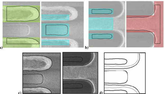
Design rules engineers need to define the enclosure margin and as a consequence need to figure out the variability of the distance between ACTIVE layer and edge of IMPLANT layer1. Figure 1 shows structures (GDS and SEM views) that will be used to illustrate this work.
(a) (b) (c) (d)
Figure 1: GDS layout with ACTIVE area in blue and IMPLANT1 in red (a); after IMPLANT1 photolithography (b); and after
complementary IMPLANT2 photolithography (c); resist aspect ratio (d)
First statement that can be done is that measuring a minimum distance between two layers is “possible” if both layers can be seen on the picture and also if both edges of the measure have enough contrast.
For the case of IMPLANT1 layer (Figure 1b), this is a “clear” mask printing mostly line features and both ACTIVE and photoresist patterns have similar contrast on the SEM image with resist pattern prone to high slope. Measuring the distance IMPLANT1 to ACTIVE (implant masking failure) seem straightforward but
measuring the coverage of resist on top of ACTIVE layer underneath (implant counter doping failure) can only be done in a deductive way.
Regarding IMPLANT2 layer, this is a “dark” layer mostly printing trenches features and in this situation due to the aspect ratio of photo resist (see Figure 1d) the image contrast of ACTIVE layer is significantly lower, making difficult any ACTIVE to Implant resist edge metrology. Like for IMPLANT1 it is not also possible to measure coverage of resist to the ACTIVE layer underneath.
3. CONTOUR EXTRACTION
The first step is to prepare for contour extraction. As mentioned previously, the two cases present different situations in term of image contrast but two layers are present on the image and GDS information must be introduced to allocate the extracted contour to the appropriate pattern on the image.
The SIMPL® software runs according to the following process flow (Figure 2) [1] where several main blocks can be identified which will be the core part of the recipe.
Contour model, calibration and calibration per “pattern / layer” which is the template of the recipe.
Contour post processing environment in which contour manipulation (alignment / stacking) is being done.
And finally the measurement template part.
Figure 2: Overview of the generic process flow for contour extraction & metrology within Aselta SIMPL® interface.
The multilayer contour extraction process will require the usage of the GDS of the measured pattern to discriminate the patterns / layers present on the image as shown figure 3.
During the contour extraction two important phases are occurring. The model calibration and the seed definition. It is possible to allocate one model and one seed per layout and therefore tune the contour extraction depending on which part of the image is being analyzed.
a) b)
c) d)
Figure 3: From SIMPL® interface, extracted contours per layer for one SEM image. GDS is used to guide and discriminate which
part of the image belongs to which layer. (a) is after Photo IMPLANT1: Green is GDS IMPLANT1, blue is ACTIVE, (b) is after photo IMPLANT2: Red is GDS IMPLANT2, blue is ACTIVE (c) is the full contour merge per image and (d) the overlap of both.
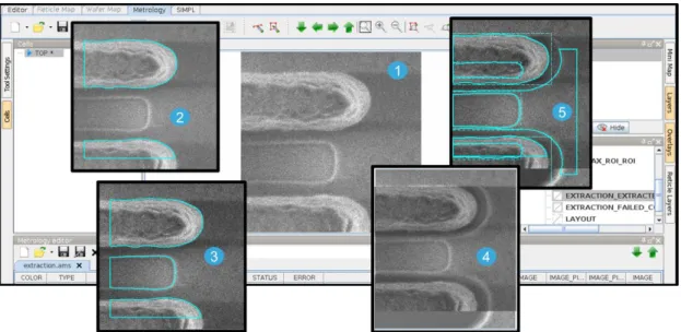
The next step is to merge these “individual” contour extraction to get a view of the complete image in multilayer mode in Figure 3c. It is possible to proceed even further by providing a multilayer and multistep view by stacking the results of both images in one environment Figure 3d. The platform has two usages. First one is to extract contour in a comprehensive way and second is to manipulate raw images, seed layers, layouts, contours in a single environment. Figure 4 shows snapshots of the results that can be viewed in the user interface. Having the capability to merge image / layouts / contours in one unique view is the first step to make measurable what is not so.
On every image it will be first necessary to compensate for SEM image centering error versus GDS fixed position. Each image will get its own shift xi / yi. Then, one or several contour extraction model might be used
depending on the contrast of each layer. The end user will choose which layer all extracted contours will have to align to, and in this case ACTIVE is the one selected. An important remark can be made here. On SEM image IMPLANT1 and IMPLANT2 not the same part of the reference layer is visible. Thanks to the capability to align to GDS it is possible align images of both steps sequences. As an alternative a SEM picture of the wafers before performing the implant lithography process could also be taken to be used as a reference.
Figure 4: Schematic overview of the contour manipulation environment process starting from Images up to merge view of here 3
different process layers. In practice each image is fully computed up to contour extraction and merge is done afterwards. (1) Starting configuration process step layer 1(ACTIVE) & 2 (IMPLANT1) (2) extraction layer 2 – here photo IMPLANT1 (3) extraction layer 1 visible part (4) overlap images process step 1 (PHOTO IMPLANT1) & 2 (PHOTO IMPLANT2) (5) full overlap of layer 1-2-3 extracted contours + GDS.
As presented in a previous paper [1], a remote contour based metrology environment can be used to provide process variability views. The concept is to reproduce what has been shown in Figure 4 but for a whole set of images. Then all the contours are stacked and aligned together with respect to the selected reference layer. This is illustrated in Figure 5.
From now onward the contour extraction analytics can start with multiple possibilities of metrology that were not possible using each individual image. A similar approach has been used by Weisbuch et al. [3], however in this case image alignment was achieved by taking a picture of the underlayer after its patterning and using the visible part of it to perform alignment of the image of the second process step. In another study [4] contour stacking and overlapping from two different process steps were performed but “overlay” errors were removed during the stacking and overlapping. Only local overlay was left. In both cases GDS were not used while in this papers this options is available.
Figure 5: Stacking of multiple contours followed by full overlap layer 1-2-3. Note that some artefacts are visible on this stacked view.
This is due to the fact that not all SEM image are perfectly centered to the pattern of interest and the re-centering in the Region Of Interest generated some truncation of images and as a consequence truncation of contours
4. CONTOUR METROLOGY
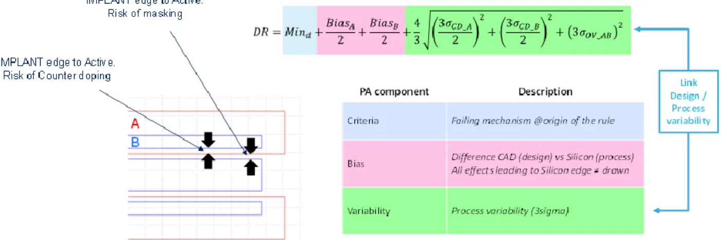
The contour data preparation work is now completed. Note that it already is an enabler to facilitate communication between various engineering communities. The resulting views are instrumental to support technical exchanges, characterization requests and process assumptions definition illustrated on Figure 6.
Figure 6: Illustration of a typical process assumption calculation used to define Edge placement tolerance (4/3 term is set here to fix
the rule at 4sigma margin, can be set to 5 for more aggressive failure)
From the equation in Figure 6 engineers derives the needs for process layer dimensional control and layer to layer overlay control. For CD this is most of the time a specific layer dimensional control which is used to feed Statistical Process Control and Run to Run control loops but it doesn’t really helps visualizing the potential direct failure mechanism. What can be done with contour-based metrology is to envision the implementation of a direct metrology dedicated to the design rule itself and reflecting the terms of the equation on Figure 6.
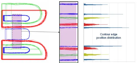
Figure 7 shows the stacked overlapped view of contours extracted from several images taken at different position on a wafer at two different process steps (photo IMPLANT1 and IMPLANT2). The measurement box in purple select the area from which the position of the edges of every single contour is extracted. A zoom of the extraction area is shown. On the right the distributions of the position of the 9 selected edges are plotted leading to a visualization of a “cross-section” of edge variability between the 3 process layers.
Combining this information with distributions of edge to edge distances as shown in Figure 8 enables a variability breakdown analysis study. Indeed, edge position distributions indicated which edge is the most variable while edge to edge distributions, for both masking and counter doping risks, indicates which gap is the most critical and where it is the most critical. Decomposition can be then done from pure dimensional control component (average + local variability) and overlay (also average + local variability). In our studied case, the counter doping risk is the highest while it is the less visible to monitor. Contour based metrology brings here the capability to see the full picture.
Figure 7: Metrology analysis window of the aggregated contours illustrated Figure5 and Edge placement distribution (on
the right) of the nine selected edge
a)
b)
Figure 8: (a) Metrology analysis using the aggregated contours revealing buried active layer under implant photoresist. Resist edge
to buried active edge distance distribution (b) Resist edge to visible active. Overlay measurement can be derived from top to bottom gap difference divided by 2.
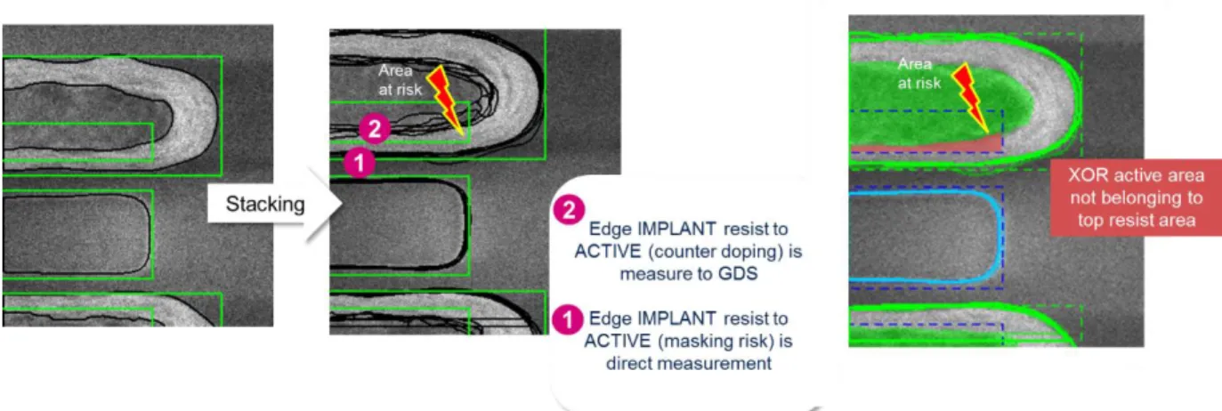
Counter doping being identified as the highest risk, the contour extraction process can be pushed further by extracting top/bottom resist profile and rounding which is relevant for implant layer.
Figure 9 shows the example for one of the implant layer from which another contour extraction model has been added to get the top of the resist shape. Knowing the nominal resist thickness an estimation of the resist slope can be extracted, which is also one of the input needed for process assumptions. By applying the same stacking & overlap process, it is here possible to visualize that a part of the active layer underneath the photo resist can be at risk regarding counter doping, since the resist doesn’t have its full thickness on top of active area (Figure 10). Any contour is able to be handled just as another layout in the interface. Therefore it is possible to perform any Boolean operation between any contour and any layer of the layout. For example, in the current use-case, it is possible to view the area at risk by simply performing a “XOR” operation of ACTIVE area within IMPLANT1 resist bottom contour not belonging to IMPLANT1 resist Top area.
Figure 9: Bottom & Top resist contour extraction plus resist Side Wall Angle metrology.
Figure 10: Overlap of CDSEM image after photolithography plus GDS layout and extracted contours (top/bottom and active area).
5. PERSPECTIVES
Contour stacking and overlapping offers many new possibilities of measurements. There is still some significant work to do to finalize an interface that is versatile enough for a large public of users. Many functionalities are still requiring dedicated scripting which is per se not compliant with a user friendly & intuitive tool. Integrating scripted functionalities as native function along with configuration interface is an
on-going process fed by many use cases at ST including the one presented in this paper. Setting up a remote platform to compute images is getting more and more traction not only from metrology engineers, but also from many other groups in the semiconductor fab. There are several reasons for this:
CDSEM are not the only tools providing images. Contour analytics can also be applied among others to XTEM, optical CD metrology tools (Figure 11a, b) with no reason to interface with other specific tooling. One unique environment for a broad range of images is definitely one purpose.
In some derivative processes, complex patterns configuration can also be addressed with contour metrology (Figure 11c), patterns that are very difficult to measure using standard SEM algorithm.
Contour extraction opens the doors to new possibilities for in-line control but the remote computing interface must be easily configurable.
Finally it is also possible to see beyond contours. Indeed, image computing is not only about contours and image quality analytics can also be developed (like blurred image detection) to sustain the contour metrology and validate a metric.
a) b) c)
Figure 11: Other example of contour metrology performed on (a) XSEM images (b) optical metrology images (c) color filter process
from image sensor (SEM).
6. CONCLUSION
This work is definitely oriented toward the construction of a contour analytics environment. If one consider that digital transformation of our activities is key, extracting more information from the many images that are collected along the silicon manufacturing control plan is one of the aspect of it.
Up to now, contours were most of the time at exclusive usage of OPC engineers. Broadening the community of contour users is instrumental for better communication and comprehension between all patterning stakeholders. For this the contour analytics environment must be simple or at least must have different level of complexity including one level accessible to end users which are not metrology specialist or OPC engineers.
The co-development of the interface is about identifying which part of contour manipulation has to be native in the interface and which part can still be custom scripts.
The use case shown in this paper already points out that it is possible to make visible things that are not and as a consequence make measurable things that are not. This is definitely helping engineers to visualize critical areas, breakdown variabilities and address appropriate solutions (design rule review, process setup changes) in a much shorter time frame.
REFERENCES
[1] B. Le Gratiet, Regis Bouyssou, J. Ducoté, Christophe Dezauzier, Alain Ostrovsky, Charlotte Beylier, Christian Gardin, Paolo Petroni, Matthieu Milléquant, Alexandre Chagoya-Garzon, Patrick Schiavone: “Contour based metrology, getting more from a SEM image”, Proc. SPIE 10959, Metrology, Inspection, and Process Control for Microlithography XXXIII, 109591M (26 March 2019).
[2] L. Schneider, V. Farys, E. Serret, and C. Fenouillet-Beranger "Framework for SEM contour analysis", Proc. SPIE 10145, Metrology, Inspection, and Process Control for Microlithography XXXI, 1014513 (28 March
2017); https://doi.org/10.1117/12.2258059
[3] François Weisbuch, Jirka Schatz, Matthias Ruhm, “Measuring inter-layer edge placement error with SEM contours”, European Mask and Lithography conference, Proc. of SPIE Vol. 10775, 107750O (2018)
[4] B. Le-Gratiet, O. Mermet, C. Gardin, S. Desmoulins, T. Kiers, Y. Wang, P. Tang, D. Tien, F. Wang, C. Prentice, W. Tel, and S. Hunsche "Investigating process variability at ppm level using advanced massive eBeam CD metrology and contour analysis", Proc. SPIE 10959, Metrology, Inspection, and Process Control for Microlithography XXXIII, 109591A (26 March 2019); https://doi.org/10.1117/12.2515242
[5] A. Lakcher; B. Le Gratiet, J. Ducoté, P. Fanton, T. Kiers, JW Gemmink, S. Hunsche, M. Besacier, C. Prentice, ” Robust 2D patterns process variability assessment using CD-SEM contour extraction offline metrology”, Proc. Of SPIE Vol. 10145-40, (2017)
[6] Amine Lakcher, Loïc Schneider, Bertrand Le-Gratiet, Julien Ducoté, Vincent Farys, Maxime Besacier, "Advanced metrology by offline SEM data processing", Proc. SPIE 10446, 33rd European Mask and Lithography Conference, 104460L (2017);
[67] Kenji Kono, Yasuo Kon, Yasunari Tsukino, Sergei Postnikov, Thiago Figueiro, Luc Martin, Paolo Petroni, and Patrick Schiavone "Demonstration of an effective mask proximity correction for advanced photomask", Proc. SPIE 10807, Photomask Japan 2018: XXV Symposium on Photomask and Next-Generation Lithography Mask
Technology, 108070A (12 June 2018); https://doi.org/10.1117/12.250178
[8] " Why we should escape a 1D-centric e-beam lithography flow"; P. Schiavone, 24th Lithography Workshop,