HAL Id: tel-02109767
https://hal.univ-lorraine.fr/tel-02109767
Submitted on 25 Apr 2019HAL is a multi-disciplinary open access archive for the deposit and dissemination of sci-entific research documents, whether they are pub-lished or not. The documents may come from teaching and research institutions in France or abroad, or from public or private research centers.
L’archive ouverte pluridisciplinaire HAL, est destinée au dépôt et à la diffusion de documents scientifiques de niveau recherche, publiés ou non, émanant des établissements d’enseignement et de recherche français ou étrangers, des laboratoires publics ou privés.
ZnSnN2 thin films for photovoltaic applications
Fahad Alnjiman
To cite this version:
Fahad Alnjiman. ZnSnN2 thin films for photovoltaic applications. Materials Science [cond-mat.mtrl-sci]. Université de Lorraine, 2018. English. �NNT : 2018LORR0296�. �tel-02109767�
AVERTISSEMENT
Ce document est le fruit d'un long travail approuvé par le jury de
soutenance et mis à disposition de l'ensemble de la
communauté universitaire élargie.
Il est soumis à la propriété intellectuelle de l'auteur. Ceci
implique une obligation de citation et de référencement lors de
l’utilisation de ce document.
D'autre part, toute contrefaçon, plagiat, reproduction illicite
encourt une poursuite pénale.
Contact : [email protected]
LIENS
Code de la Propriété Intellectuelle. articles L 122. 4
Code de la Propriété Intellectuelle. articles L 335.2- L 335.10
http://www.cfcopies.com/V2/leg/leg_droi.php
THÈSE
Pour l’obtention du titre deDOCTEUR de L’UNIVERSITÉ DE LORRAINE
Spécialité : Physique – Nanoscience
Présentée par
Fahad ALNJIMAN
ZnSnN
2
thin films for photovoltaic
applications
Soutenance publique prévue le 21 Décembre 2018 à Nancy devant le jury composé de :
Angelique BOUSQUET Rapporteur Maitre de conférences – HDR, Institut de Chimie de Clermont-Ferrand, Université Clermont Auvergne – CNRS
Thomas FIX Rapporteur Chargé de recherche - HDR, Laboratoire ICUBE, Université Strasbourg – CNRS
Marie-Paule BESLAND Examinateur Directeur de recherche, Institut des Matériaux de Nantes Jean Rouxel, Université de Nantes – CNRS
Frederic SANCHETTE Examinateur Professeur, Institut Charles Delaunay, Université de Technologie de Troyes – CNRS
Jean-François PIERSON Co-directeur de thèse Professeur, Institut Jean Lamour, Université de Lorraine – CNRS
Patrice MISKA Directeur de thèse Maître de Conférences - HDR, Institut Jean Lamour, Université de Lorraine – CNRS
Institut Jean Lamour, UMR 7198, ARTEM - CS 50840-54011 Nancy Cedex Université de Lorraine – Ecole doctorale Chimie - Mécanique – Matériaux- Physique (C2MP)
ﻢﯿﺣﺮﻟا ﻦﻤﺣﺮﻟا ﷲ ﻢﺴﺑ
ًﻞﯿِﻠَﻗ ﱠﻻِإ ِﻢْﻠِﻌْﻟا َﻦﱢﻣ ﻢُﺘﯿِﺗوُأ ﺎَﻣَو
To my family
To my Mother
Acknowledgements
First, I would like to express my sincere gratitude to my supervisor Mr Patrice Miska for the continuous support of my Ph.D work and for our discussion, his patience, motivation, enthusiasm and knowledge.
Also, I wish to express my gratitude to my co-supervisor(frero) or my big brother Pr.Jean-François Pierson for providing me the opportunity to develop this work. He was always willing to share any ideas with me. Only through his fruitful discussion, strong experience and hard work, the completion of this thesis became possible.
I would like to thank to the members of the jury for agreeing to participate in my PhD defense.
A very special thanks goes out to Mr. Jaafar Ghanbaja, Ms. Stéphanie Bruyere, Ms. Sandrine Mathieu and Ms. Christine Gendarme for their important contribution during my PhD thesis.
I also want to express my great thanks to Ms. Sylvie Migot for his TEM sample preparation by FIB always in a short time.
Also, A very special thanks goes out to Mr. Sébastien Diliberto and Mr. Pascal Boulet for their important contribution during my PhD thesis
In the case of administration, I am grateful for the help from Valérie Tamburini, Valérie Madeline and the big boss Thierry Belmonte.
Special thank to Mr. Abdelkrim Redjaïmia for the discussions.
I would like to start to thanks all my friends in the lab and I hope that I will not forget one of them : First, I will start with PVD dream team, David Pilloud, Silvère Barrat, Alan Corvisier, Fabien Capon, David Horwat, Alaa Eldin Giba, Benjamin Gilbert, William Chamorro, Manuel Tresse, Martin Mickan, Emile Haye, Claudia De Melo Sanchez, Alejandro
Borroto, Alexis Garcia Wong, WANG Yong, Agathe Virfeu, Christophe Celindano, Joseph Antoine, Nicole Beddelem, Daria Kharkhan, Christy Fadel, Aurelien Didelot, Aurelien Etiemble and Osama Madkhali.
A very special thanks to Kosseila Ait Oukaci, Dorra Ibrahim, Hiba Kabbara, Saïma Siouane, Turki Alshammari, Osama Madkhali, Mahmoud Trad, Soufiane EL OUALID, Selma Sassi, Enaam Jamal Al Dine, Meriem Ben Haj Slama, Ziad Al Hallak, Zied Ferjaoui, Firas Abdel Hamid, Brigitte vigolo, Pascale Corne, Tom Ferte, Pauline Vilasi, and Abdallah Imam. All my friends from Saudi Arabia here in Nancy and all of my friends there.
Thanks the lab Institut Jean Lamour to give me the access to use so many equipments. Thanks the Saudi Arabia Embassy in France for the PhD grant.
Finally, I would like to thank my wife for sharing and spurting all the moments of study also my brother Majed and all my family. Thanks to my father. Also thanks to part of my heart Mohammed, Zainab and Youssef.
Contents
General introduction ... 1
Chapter 1. Zinc tin nitride: a new material with large applications for photovoltaics ... 5
1.1 Introduction ... 5
1.1.1 Context, Positioning and Objectives of the Work: The Need of New Material Developments ... 5
1.1.2 The Question of Realization Complexity and Indium Supply Shortage vs. Industrial Needs 5 1.1.3 Photovoltaics concerns ... 6
1.1.4 PV technologies ... 7
1.2 Potentialities of New ZnSnN2 Material Physical Properties ... 10
1.2.1 ZnSnN2 historical aspects: an overview ... 11
1.2.2 Focus on the issue of the crystal structure. ... 14
1.2.3 The issue of the electronic structure, defects and band gap ... 19
1.3 Conclusion ... 23
References ... 25
Chapter 2. Synthesis of zinc tin nitride thin films and characterization methods ... 31
2.1 Introduction ... 31
2.2 Zinc tin nitride thin film growth ... 31
2.3 Structure zone diagram (SZD) ... 33
2.4 Elaboration setup ... 34
2.5 X-ray diffraction (XRD) ... 35
2.6 X-ray energy dispersive spectroscopy (EDS) and scanning electron microscopy (SEM) ... 37
2.7 Conversion electron Mössbauer spectroscopy ... 38
2.8 Transmission electron microscopy (TEM). ... 40
2.9 Four-point probe method ... 41
2.10 Hall effect measurements ... 42
2.11 UV-visible spectroscopy ... 43
2.12 Ellipsometry ... 46
2.13 X-ray photoelectron spectroscopy (XPS) ... 47
2.14 Conclusion ... 48
References ... 49
Chapter 3. ZnSnN2 Thin Films: Synthesis and characterization ... 53
3.1 First attempt to grow zinc tin nitride thin films by PVD ... 53
3.1.2 Growth of ZnSnN2 by fixing the discharge voltage ... 55
3.1.3 Growth of ZnSnN2 by controlling the discharge voltage in a pure nitrogen plasma. ... 57
3.1.4 Effect of the substrate nature ... 60
3.2 Crystalline ZnSnN2 thin films structure, microstructure, physical and chemical properties ... 61
3.2.1 Introduction ... 61
3.2.2 Chemical composition ... 62
3.2.3 Structure of ZnSnN2 films ... 62
3.2.4 Microstructure and morphology of ZnSnN2 thin films ... 64
3.2.5 X-ray photoelectron spectroscopy analysis of ZnSnN2 thin films ... 68
3.2.6 Mossbauer spectrometry of ZnSnN2 thin films ... 70
3.2.7 Electrical and optical properties of ZnSnN2 ... 71
3.3 Effect of base pressure before the film growth ... 76
3.4 Conclusion ... 82
Reference ... 84
Chapter 4 Microstructure and tuning the structure of ZnSnN2 thin films ... 91
4.1 Focus on the structure of ZnSnN2 ... 91
4.1.1 Orthorhombic, monoclinic or hexagonal structures ... 91
4.1.2 Monoclinic vs orthorhombic ... 92
4.1.3 Monoclinic versus hexagonal phases ... 95
4.2 Tuning the structure of ZnSnN2 ... 98
4.2.1 Tuning the structure with the stoichiometry ... 98
4.2.2 Tuning the structure by changing the pressure ... 103
4.3 Conclusion ... 113
References ... 117
1
General introduction
The development of renewable energy sources is of an outmost importance for our societies. It is also a political issue due to the global warming. The optoelectronic industry is growing mainly based on the use of specific class of materials. If the classical GaN UV LEDs are well mastered, it is important to find and develop alternative materials. Such demand is also growing in the field of photovoltaic. Solar energy will be one of the main part of renewable energy system. To fulfil the challenging issues and to develop new markets the discover of new materials is essential.
III-V materials are commonly used as active layers in LEDs, transistors, solar cells and mechanical devices. The main spinneret is based on the use of InGaN alloys. However, such layers contain indium and gallium. Significant volatility in their price and supply over the past years has led to considerable concern given their critical roles and their use in a wide range of large-scale electronic devices. Moreover, at present the crystalline III-V materials require the use of epitaxial growth techniques with high cost and high complexity. It is important to study and develop new earth abundant materials with optimized properties for the realization of innovative optoelectronic devices that could be competitive cost for mass production.
In this work, we aim at developing a new kind of inexpensive, indium/gallium-free, nitride material. It could be the basis of new way for optoelectronic applications. The study of such very innovative material is an ambitious goal but has already started in various countries (China, India, USA) with different groups involved. The studies are focusing on the family of Zn-IV-N2 alloys that is promising as its bandgap energy could span the solar spectrum and could then replace the InGaN alloys. We have chosen to use reactive magnetron sputtering that is an easily up-scalable production technique with a quite low cost.
Nonetheless, data about these ZnSnN2 alloys remain scarce and sometimes contradictory. Numerous efforts remain to be done to better understand its fundamental properties. For example, the crystallographic structure of the material is not clearly defined. Additionally, ZnSnN2 alloys seem to be difficult to control by PVD growth. All these aspects are studied in this work.
In the first chapter of this manuscript we will describe the large context of photovoltaic and few related concerns. Then, we will describe the solutions proposed in literature more especially by developing new materials. Among the recent suggestion found in literature, the
2
ZnSnN2 alloy seems to be a good candidate. We will also describe the state of the art about the materials by showing the key points as well as the work that remain to be done.
In the second chapter of this manuscript we will describe the growth and characterization techniques used in this work and that are, for most of them, available on site at the Institut Jean Lamour.
The third chapter is dedicated to the first set of results. After a description of the optimization of the growth process, we will show the results focused on a first approach of the growth at room temperature of highly crystallized ZnSnN2 thin films. Then we study the effect of the base pressure of the chamber on the structure and the properties of ZnSnN2 thin films.
The fourth chapter is a focus on the film analysis by high-resolution transmission electron microscopy and electron diffraction. We used the top facility we have at the Institut Jean Lamour to determine the film structure. The second part of this chapter is dedicated to the effect of the film stoichiometry and the total pressure on the films properties.
3
Chapter 1. Zinc tin nitride: a new material with large
applications for photovoltaics
... 51.1 Introduction ... 5
1.1.1 Context, Positioning and Objectives of the Work: The Need of New Material Developments ... 5
1.1.2 The Question of Realization Complexity and Indium Supply Shortage vs. Industrial Needs ... 5
1.1.3 Photovoltaics concerns ... 6
1.1.4 PV technologies ... 7
1.2 Potentialities of New ZnSnN2 Material Physical Properties ... 10
1.2.1 ZnSnN2 historical aspects: an overview ... 11
1.2.2 Focus on the issue of the crystal structure. ... 14
1.2.3 The issue of the electronic structure, defects and band gap ... 19
1.3 Conclusion ... 23
5
Chapter 1. Zinc tin nitride: a new material with large applications for
photovoltaics
1.1 Introduction
1.1.1 Context, Positioning and Objectives of the Work: The Need
of New Material Developments
The development of alternative materials for photovoltaics has attracted much attention over the last decade and is currently of a crucial importance for our society. A reliable plan for the development of carbon free energy supply has become inevitably important for policy makers in many states all over the world. Regarding the societal context, many research programs are dedicated to new material discovery over the world. I will describe here these aspects.
1.1.2 The Question of Realization Complexity and Indium Supply
Shortage vs. Industrial Needs
Although the InGaN route can be promising, large scale III-V (InGaN and InGaAsP) based devices will be limited by the quality of the material (indium incorporation in InGaN for example) but also by the growth technique used (epitaxy). Moreover, the reliance on indium and gallium, with its limited economically viable sources, could potentially limit its long term use in large-scale solar devices. Indeed, indium is primarily and profusely used in TCO for flat screens.
6
Figure 1.1 Abundance of elements in the Earth’s crust as funtion of their atomic number[1].
The question of the material availability is exposed in many reports. (Figure 1.1) shows for example the abundance of different element in the Erath’s crust. The indium is one of the scarcer elements. Indium reserves are then estimated at twenty years at current production rates. Indium recovery processes exist but are of little eco-friendly and energy-intensive concerns. Beyond questioning about its availability, a significant increase in indium price is to be feared due to speculation on raw materials observed in recent years. It is then of utmost importance to develop materials with earth abundant and using large scale growth methods.
1.1.3 Photovoltaics concerns
As the topic of this manuscript is dedicated to materials that could be useful for photovoltaic technologies, it is interesting the give a short description of the frame and of the needs in this field.
The energy demand is still increasing over the world and has reached 13 800 millions of oil equivalent tons according to a study from the International Energy Agency [2]. Among the current offer, a large part of the energy production uses non-renewable resources such as oil, coal, or uranium. On the contrary, the photovoltaic market is now under-developed with a rate of 1.2% of the electricity production. However, this market is rapidly growing because of the policies of the states. A 420 GigaWatts production capacity is now available and the market is growing with a rate of 25% per year (Fig. 1.2)[3].
7
Figure 1.2 Global capacity of solar photovoltaic by some country and region[3].
Nevertheless, efforts still must be done to reach the global objectives of green energy production and for decarbonized energy generation. Among the possibilities, the production of green photovoltaic electricity is deeply studied. Indeed, the energy coming from the sun, an abundant and free source, can be considered as green if the sun energy harvesting technologies can be ecological. This point requires the photovoltaic technology competitiveness improvement to reduce the cost of the electricity produced and to take care of the ecological footprint of technologies used.
1.1.4 PV technologies
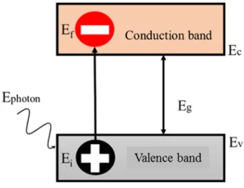
In 1839, a French physicist Edmond Becquerel had discovered the photovoltaic effect and he created the first photovoltaic cell in the world[4]. The principle of the photovoltaic is to convert the sunlight into electricity. Absorption of a photon in a material means that its energy is used to excite an electron from an initial energy with level Ei from valence band to a higher energy level Ef in conduction band as shown in Fig. 1.3. The photon energy must be can greater than the band gap energy Eg in order to create an electron-hole pair.
8
Figure 1.3 Generation of an electron-hole pair by absorption of a photon.
However, there are five main categories of solar cells. They are classified according to the materials used and the fabrication methods. The National Renewable Energy Laboratory (NREL) published every year the best research cell efficiencies charts that includes the evolution with the year for the five main categories shown in fig. 1.4.
9 The five main categories are:
1. Multijunction cells. 2. Single-junction GaAs. 3. Crystalline Si cells. 4. Thin-film technologies. 5. Emerging PV concepts.
Among the possible solar cells, the multijunction one is the most efficient and has the current world record. The multijunction solar cell has multiple p–n junctions made with different semiconductor materials. Each junction creates an electric current in response to different wavelengths of the incoming light. The use of multiple semiconducting materials allows then the absorbance of a wide range of wavelengths. However, the multijunction solar cells have achieved the highest efficiencies performance of approx. 46% [6]. An example for multijunction solar cell shown in Fig. 1.5.
10
The main problem of this kind of device is its elaboration complexity and the use of materials containing In and Ga as mentioned in section 1.1.2.
Another approach lies in the use of new materials such as CuInGaS2(Se2) (CIGS). Such an approach has been widely developed in the last 10 years but the efficiencies are still low, around 22 % in laboratory for a 0.5 cm2 cell with CIGS[7]. Moreover, CIGS cells contain indium that scarcity issue is a real problem. Additionally, these other technologies, that are in front competition with the c-Si one, are also suffering serious problems of toxicity by needing the use of alternative layers containing Cd or scarcity (Te-0.005 ppm and Se-0.05 ppm) for possible TW-scale deployment. Then different alternatives and more or less fruitful solutions have been proposed over the last years to replace the CIGS technology such as the development of I2-II-IV-VI4 materials like e.g. Cu2ZnSnS4 (CZTS). This could be a real interesting approach but unfortunalety the efficiencies are also still low around 12%.
Finally, among the emerging technologies, we can quote the organic-inorganic perovskite materials. The efficiency of perovskite is rising today but the highly efficient stable and lead-free perovskite material route constitutes however the strongest challenging way. If the efficiencies are high, the stability of the perovskite is currently low and the realization of a stable device still requires a lot of work, until Turren-Crus [8] on 11-oct-2018 prove and demonstrate the perovskite solar cells are stable with high-performance.
1.2 Potentialities of New ZnSnN
2Material
Physical Properties
In a first approach focused on the study of new materials we would like to open a complementary route using nitrogen based materials. Following the inorganic thin film strategy where the III-N materials have already been proven to be very stable, it is so natural to focus on a still poorly investigated semiconductor material line closely related to the (In,Ga)N family and for which the column III element is replaced by an ordered cation sublattice composed of equal numbers of Zn and column IV (Si, Ge, Sn) atoms.
Zinc tin nitride (ZnSnN2) is the last compound studied from the family of Zn-IV-N2 semiconductors, where the IV element can be (Si-Ge-Sn). This compound of Zn-IV-N2 is closely related to the III-N semiconductors [9],[10] where elements III are (Al-Ga-In). The family of III-nitrides are promising materials for semiconductor devices applications, more especially for optoelectronic applications for a wide range of photon energies. These compounds have optical band gaps of 6.2 eV for AlN, 3.4 eV for GaN and 0.7 eV for InN [11].
11
Furthermore, what is make these compounds are interesting is the possibility of tuning of the band gap through alloying of IIIx-III1-x-N. For example AlxGa1-xN is a wide bandgap semiconductor reaching the band gap range from 6.2 eV to 3.4 eV by changing the ratio between Al and Ga [12]. The same property is obtained for InxGa1-xN with the possibility to tune the band gap range from 3.5 eV and 0.7 eV by using different ratio between In and Ga [13]. Quayle P. et al [14] have compared the band gap energies between these two nitrides families: III-N and Zn-IV-N2. They reported the band gaps energies versus the material lattice constant (figure 1.6). Such a representation shows the possibility to get adjustable band gap for Zn-IV-N2, which is then a potential good candidate for replacing the III-N materials.
Figure 1.6 The band gaps versus “a” lattice constants for III-nitrides and Zn–IV-nitrides and their alloys.[14].
1.2.1 ZnSnN
2historical aspects: an overview
ZnSnN2 is a semiconducting material belonging to the family of Zn-IV-N2. By changing the IV elements from (Si-Ge-Sn) the band gap and the lattice parameter can be tuned. Historicaly, Maunaye et al. [15] first reported in 1970 the growth of this kind of material, precisely ZnGeN2. In 1992 Endo et al [16] reported the first growth of ZnSiN2 by using high-pressure synthesis.
So far, only ZnGeN2 and ZnSiN2 alloys have been synthesized and relatively well characterized. As an example we can mention the growth of ZnSiN2 by MOCVD [17] on
12
sapphire or SiC substrates. Greater efforts have been devoted to ZnGeN2: single crystals were obtained by VLS method, thin films were deposited on glass and silicon spray radiofrequency and MOCVD were used for growth on sapphire and SiC [18]
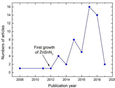
For ZnSnN2 after the first publication related to the growth of ZnSnN2 in 2011, the numbers of article published per year has increased as shown in figure 1.7 with data extracted from Web of science [19].
We can mention that ZnSnxGe1-xN2 grown by RF sputtering have also shown a real potential for photonic and optoelectronic application, results published in 2015 by A. M. Shing
et al. [20].
Figure 1.7 Number of articles on ZnSnN2 published per year based from web of science up to date
18/12/2018.
Experimental studies on ZnSnN2 are scarcer and the properties of this material are not well known. The first theoretical study has been realized by Paudel et al. [9] in 2008.
The first ZnSnN2 developments in 2011 by N. Feldberg, et al. [21] show very interesting and encouraging results. In their study, the material is deposited using a molecular beam epitaxy process. The first experimental results in 2011 [21] and a theoretical study by A. Punya et al. [10] explicitly evoked the interest of ZnSnN2 for optoelectronics.
In 2013, the California Institute of Technology published quite interesting results by L. Lahourcade et al. [22]. In particular, the authors presented some optical properties of ZnSnN2 films obtained by sputtering and exhibiting an experimental band gap of 1.8 eV (Figure 1.8) which is in opposition to the theoretical prediction of 1.42 eV. The authors explain this
13
deviation with the existence of Burstein-Moss effect due to a significant n-type doping of the order of 1021cm-3. However, this issue remains to be clarified.
Figure 1.8 (a)Bandgap as a function of the carrier concentration, (b) evaluation of the bandgap
and absorption coefficient of ZnSnN2 by optical measurements [22].
Another study in 2013 also provides some theoretical and experimental optical data of ZnSnN2 obtained by molecular beam epitaxy assisted by nitrogen plasma [23]. However, the authors contradict the results of the first two studies mentioned above about the crystallographic structure. They found it has a monoclinic structure instead of an orthorhombic as predicted. This change in the crystalline structure impacts the bandgap energy but the question remains open. They also predict the possibility of reducing the forbidden band gap to 0.95 eV related to the cationic disorder, which may allow a greater tuning of the bandgap of the material.
In 2015, a study from a Chinese group has reported electron concentration between 2.3x10¹⁷ and 1.6x1018 cm-3 with band gap estimated in the 1.82-1.95 eV range [24]. This group also revealed that the useful absorption range of the ZnSnN2 compound is comparable to those of InP, CdTe and GaAs materials (Figure 1.9).
14
Figure 1.9 Plots of the AM1.5 solar spectrum and the absorption coefficient, comparing the
evaluation of the bandgap and absorption coefficient of ZnSnN2 with others materials [24].
In 2015, carrier densities of 1.8x10¹⁸ and 4.5x1020 cm-3 with the highest mobility being 8 cm2 V-1S-1 have been reported. The authors also reported for the first time the possibility of doping control in ZnSnN2 through varying cation off-stoichiometry [25].
In 2015 again, a paper published by Veal et al. showed the possibility to allow the bandgap variation between 1.33 and 2.38 eV by tuning the degree of cation disorder by varying the growth condition using plasma-assisted MBE [26].
Recently, a Chinese group has reported the high resistivity behavior of ZnSnN2 sputtered films and also demonstrated satisfactory PN junction I(V) curve which is really encouraging for PV device realization R. Qin et al.[27].
1.2.2 Focus on the issue of the crystal structure.
ZnSnN2 is a semiconductor material that is one of the family of II-IV-N2. The crystal structure for this new family is considered as wurtzite structure with overall orthorhombic symmetry. T. R. Paudel et al. in first-principles study of phonons and related ground-state properties and spectra in Zn-IV-N2 compounds defined the ideal structure as wurtzite structure with overall orthorhombic lattice vectors 𝑎, 𝑏 and 𝑐 [9]. Those vectors are related with the wurtzite lattice vectors 𝑎), 𝑏) and 𝑐) by 𝑎 = 𝑎), 𝑏 = 𝑎)+ 2𝑏) and 𝑐 = 𝑐).
For ZnSnN2 the most stable and accepted crystal structure is orthorhombic (fig. 1.10) with 16 atoms per unit cell, 4 atoms of zinc, 4 atoms of tin and 8 atoms of nitrogen. The group
15
space for the orthorhombic is Pna21 which is known for β-NaFeO2 or in general a I-III-VI2 compound. By DFT calculations T. D. Veal et al. [26] have defined the difference between the two structures of the orthorhombic and wurtzite by the ordering in the cation sublattice of ZnSnN2. Orthorhombic structure has cation-ordered while the wurtzite one has fully-disordered-cation sublattice.
Figure 1.10 Orthorhombic crystal structure of ZnSnN2 along different directions.
The wurtzite structure of ZnSnN2 is close to the III-nitride (Al,Ga,In)-N material with hexagonal lattice and space group P63mc. This structure is known to be that of ZnO. As we mentioned before the wurtzite structure of ZnSnN2 correspond to disorder cation position with randomly located Zn and Sn atoms. (Figure 1.11).
16
Figure 1.11 Hexagonal crystal structure of ZnSnN2 along different directions.
However, one of the critical challenge is the understanding of the crystal structure of this material. Data extracted from literature and reported in table 1 gathered the information from the debate of previous works of ZnSnN2. The debate is focused on the discussion about the nature of the crystal structure. Nine articles reveal calculations and experimental results showing an orthorhombic structure and seven articles describe a wurtzite one. However, an additional article has described a monoclinic structure but we can see in table 1 that the lattice parameter was very close to the hexagonal structure. Whatever the structure described in the literature, there is no discussion on the effect of the deposition parameters that may favor one specific structure. Indeed, most of the processes used in the literature are not at the thermodynamic equilibrium. Then, metastable structures may be formed.
17
Table 1. Crystallographic results of ZnSnN2 in the previous works.
Structure Calculated parameters (Å) Experimental parameters (Å) Reference 𝑎 𝑏 𝑐 𝑎 𝑏 𝑐 Orthorhombic 6.76 5.85 5.58 - - - [9] Orthorhombic 6.76 5.85 5.58 - - - [10] 6.59 5.70 5.41 6.70 5.80 5.53 Monoclinic - - - 3.395 3.400 5.534 [21] 𝛼 = 89.885° 𝛽 = 90.033° 𝛾 = 120.036° Orthorhombic - - - 5.842 6.753 5.462 [14] Orthorhombic 6.755 5.846 5.473 [23] Orthorhombic 6.721 5.842 5.459 - - - [22] Orthorhombic - - - 5.853 6.741 5.498 [24] Wurtzite - - - - [28] Orthorhombic - - - 6.721 5.842 5.459 Wurtzite - - - 6.755 5.846 5.473 [26] Wurtzite - - - [29] Orthorhombic 6.812 5.914 5.542 6.885 5.955 5.577 [30] Wurtzite - - - 3.366 3.366 5.842 Orthorhombic - - - 5.842 6.753 5.464 [31] Wurtzite - - - 3.376 3.376 5.467 Wurtzite - - - [27] Wurtzite - - - 6.885 5.955 5.577 [32] Orthorhombic - - - 3.366 3.366 5.842 Orthorhombic 6.82 5.91 5.54 [33] Wurtzite - - - 3.366 3.366 5.842 [34]
The fig. 1.12 presents the theoretical peak positions of X-ray diffractograms for the 3 structures of ZnSnN2. As shown in this figure, the main diffraction peaks are superposed. for these structures The black ones correspond to the hexagonal structure with lattice parameter a = 3.41 Å, c = 5.11 Å, In red are the monoclinic structure with lattice parameter a = 3.39 Å, b = 5.54 Å, c = 3.36 Å and b =119.136°, and in blue are the orthorhombic structure with lattice parameter a = 5.84 Å, b = 6.89 Å and c = 5.52 Å. This figure clearly evidence that is is hard to distinguish the structure of ZnSnN2 films from X-ray diffraction.
18
Figure 1.12 Peak positions calculated for 3 different structures. The black ones correspond to the hexagonal structure with lattice parameter a=0.341 nm c=0.511 nm, the red one correspond to the monoclinic structure with lattice parameter a=0.339 nm, b=0.554 nm, c=0.336 nm and b=119.136°,
and the blue one are related to the orthorhombic structure with lattice parameter a=0.584 nm ,b=0.689 nm and c=0.552 nm.
The figure 1.13 shows the electron diffraction pattern simulation of three structures that can be encountered for ZnSnN2. As for the XRD, the electron diffraction does not seem to be the more powerful method to distinguish the 3 main structures previously described for ZnSnN2 in the literature.
19
Figure 1.13 Theoretical electron pattern for 3 different structures,(a) Electron diffraction pattern
simulation for monoclinic structure P21 in zone axis [001], (b) Electron diffraction pattern
simulation for hexagonal structure P63mc in zone axis [010], (c) Electron diffraction pattern
simulation for orthorhombic structure Pna21 in zone axis [010].
The question of the crystallographic structure is so still in debate and the question remains open.
1.2.3 The issue of the electronic structure, defects and band gap
ZnSnN2 is a n-type semiconductor which has a theoretical direct band gap ranging between 1 and 2 eV depending on the cation disorder [21] [23]. As already mentioned in the crystal structure in section 1.2.2, there are two main expectations for the structure of ZnSnN2. The orthorhombic structure has a cation-ordered while the wurtizte structure has a fully-disordered-cation sublattice.
By using DFT calculations, N. Feldberg et al [23] have shown that for the perfectly ordered orthorhombic lattice at zero Kelvin the band gap of ZnSnN2 is 2.09 eV, while the
20
calculated band gap of the disordered monoclinic one is 1.12 eV. T. D. Veal et al [26] experimentally confirmed this behavior by growing ZnSnN2 with different parameters by MBE with a good control of the cation ordering in the film. They have obtained a band gap varying in the range 1.33 - 2.38 eV which is an excellent agreement with the DFT results obtained by N. Feldberg et al [23]. The shift of the band gap between the calculated and the experimental data could be explained and interpreted as a Burstein–Moss shift due to high carrier concentration in the film (Figure 1.14).
Figure 1.14 Burstein-Moss effect.
L. Lahourcade et al. [22] by using DFT method with an hybrid functional HSE (Heyd-Scuseria-Ernzerhof) at zero Kelvin have calculated a direct band gap of 1.42 eV for an orthorhombic structure in the most stable space group Pna21. Experimentally, by using spectroscopic ellipsometry, they obtained an optical band gap value near 2.0 eV. Here again, the difference with theoretical results can be attributed to the Burstein-Moss effect due to the high electron carrier concentrations measured by Hall effect. In the table 2 are summarized some data band gap values extracted from previous works of ZnSnN2.
21
Table 2. Band gap results of ZnSnN2 in the previous works
Band gap Calculation
method Experiment method Structure Reference
2.02 eV QSGW - Orthorhombic [10] 2.0 eV DFT - Orthorhombic [21] 2.1 eV Transmittance Monoclinic 2.09 eV DFT - Orthorhombic [23] 1.12 eV DFT - Monoclinic 2.12-2.38 eV Transmittance Orthorhombic 1.7 eV Photoluminescence Orthorhombic [14] 1.42 eV DFT hybrid functional - Orthorhombic [22]
2.0 eV spectroscopic ellipsometry Orthorhombic
1.8 eV QSGW - Orthorhombic [35]
1.9 eV spectroscopic ellipsometry Orthorhombic [24]
1.0 eV UV-Vis-NIR spectroscopy Wurtzite [28]
1.81 eV QSGW - Orthorhombic [36]
1.4 eV Transmittance Orhto/wurtzite [31]
1.64 eV - Wurtzite [27]
1.75 eV DFT - Orthorhombic [37]
2.62 eV PBE0 - Orthorhombic [27]
As well, Hall effect measurements has been used for ZnSnN2 to measure the electron carrier concentrations and the electron mobility. As already mentioned, the Burstein-Moss effect may appear in ZnSnN2 thin films due to the highest electron carrier concentrations. The values of electron carrier concentrations given in literature vary over a wide range.
The first report of the electron concentration measurements in ZnSnN2 is given by Lahourcade et al. [22] for ZnSnN2 grown by RF sputtering. They obtained an electron concentration in the 5x10¹⁹ - 1021 cm-3 range. In this work, they mentioned the Burstein-Moss effect due to this large electron concentration. They were also expecting to have a high electron mobility. However, the electron mobility was about 10 cm2 V-1s-1, this low mobility has been attributed to the small grain size, which is usual for the materials grown by sputtering.
Other work by Feldberg et al. [23] have measured the mobility and the electron concentration of ZnSnN2. They have been grown the films by molecular beam epitaxy. They obtained a measured mobility about 10 cm2 V-1s-1 and the electron concentration is in the
22
3.0x10²⁰ and 1.1x1021 cm-3 range. They also mentioned to Burstein-Moss shift phenomenon in the material.
In other cases, ZnSnN2 have been grown by using DC sputtering by Deng et al. [24]. The authors measured the mobility and the electron concentration after annealing the film in a N2 atmosphere at 300 and 400 °C. They obtained an electron concentration reduction from 1.0x10¹⁸ to 2.3x1017 cm-3 and a mobility decrease from 3.98 to 1.86 cm2 V-1s-1 as the annealing temperature increases. As well, Qin et al. [27] have grown ZnSnN2 by DC-sputtering and they measured the electrical propriety after annealing at 200, 300 and 350 °C. They obtained mobilities between 0.37- 2.07 cm2 V-1s-1 and electron concentrations between 2.77x10¹⁷ and 6.78x1017 cm-3.
Figure 1.15 Evolution of the carrier densities with years [38].
Finally, Fioretti et al. [28] have grown ZnSnN2 by using RF-sputtering. They measured the mobility and the electronic concentration as a function of the stoichiometry. Mobilities between 1.1 – 8.3 cm2 V-1s-1 and carrier densities between 2x10¹⁸ – 2x1020 cm-3 were obtained and the lowest carrier concentration was reached with the off-stoichiometry sample with 0.70 =Zn/(Zn+Sn). In 2017, Fioretti et al. [39] have achieved the lowest value of the carrier concentration for zinc rich ZnSnN2 thin film by growing this material in forming gas H2/N2 and then annealed in atmosphere of nitrogen for 6 h at 300 °C. With this method, they obtained a value 4 x 1016 cm-3 which is the lowest described the literature for ZnSnN2 ever. On the other
23
hand, they remarked that the electron mobility decreases from 5-8 to less than 1 cm2 V-1 s-1 with annealing. They thought the decrease in mobility might be related to an increase in the ionized impurity scattering due to an increase in activated acceptors.
Few groups succeed to growth ZnSnN2. As we mention before Feldberg et al. [21] was the first growth of ZnSnN2 where they grow this compound by using plasma-assisted molecular beam epitaxy. Lahourcade et al. [22] have grown ZnSnN2 by RF sputtering. A few years later Veal et al. [26] have also grown ZnSnN2 by using MBE. Quayle et al [14] synthesised this compound by using plasma-assisted vapor liquid solid technique. By using DC sputtering Dang
et al [24] have grown ZnSnN2 thin film. Fioretti et al. [28] in 2015 achieved to synthesis ZnSnN2 by using RF-sputtering. Kawamura et al. [31] have synthesised this compound in bulk form via a high-pressure-metathesis reaction. Finally, Kuo et al. [24] have succeed to grow this compound in 2017 by using combinatorial approach.
1.3 Conclusion
This first chapter was a bibliographic introduction to the topic of the thesis work. We presented the issues of Earth abundant materials and of scarcity of some elements. Then, we turned to the issue of the energy need and more especially the question of the production of energy, the sun being a real opportunity as it is a free source of energy coming on Earth. The photovoltaic technologies are under development but the different approaches suffer from material or technological problems to be overcome if we want to produce electricity by using a green technology, that is to say with cheap mass production possibilities and without scarce materials.
Then, we described the new material we would like to study: ZnSnN2. We showed the main advantages for photovoltaic objectives but we also stressed that a lot of work remains to be done for a good understanding of the material properties and for a good control of the growth process. More especially, we underlined that the crystallographic structure remains not well known in literature.
The aim of this work is then to bring new insight about the growth and the physical of ZnSnN2 films grown by PVD. It is a topic with a lot development to be done but that may be studied at Institut Jean Lamour as a lot of dedicated facilities are present more especially around material analysis. These facilities will give a chance to bring new element that maybe able answer some unsolved questions during this work.
25
References
[1] « Rare Earth Elements—Critical Resources for High Technology | USGS Fact Sheet 087-02 ». [En ligne]. Disponible sur: https://pubs.usgs.gov/fs/2002/fs087-02/. [Consulté le: 05-avr-2018].
[2] « Key World Energy Trends 2016,” tech. rep., International Energy Agency (IEA), 2016 ». .
[3] « Photovoltaics-Report.pdf ». .
[4] E. Becquerel, « Mémoire sur les effets électriques produits sous l’influence des rayons solaires », in Sci. Paris, vol. 9 (1839) 561, .
[5] « efficiency-chart.png (1200×665) ». [En ligne]. Disponible sur: https://www.nrel.gov/pv/assets/images/efficiency-chart.png. [Consulté le: 12-avr-2018]. [6] F. Dimroth et al., « Four-junction wafer bonded concentrator solar cells », 2015, p. 1- 1. [7] F. Karg, « High Efficiency CIGS Solar Modules », Energy Procedia, vol. 15, p. 275- 282, janv. 2012.
[8] S.-H. Turren-Cruz, A. Hagfeldt, et M. Saliba, « Methylammonium-free, high-performance and stable perovskite solar cells on a planar architecture », Science, p. eaat3583, oct. 2018.
[9] T. R. Paudel et W. R. L. Lambrecht, « First-principles study of phonons and related ground-state properties and spectra in Zn-IV-N2 compounds », Phys. Rev. B, vol. 78, no 11, p. 115204, sept. 2008.
[10] A. Punya, W. R. L. Lambrecht, et M. van Schilfgaarde, « Quasiparticle band structure of Zn-IV-N2 compounds », Phys. Rev. B, vol. 84, no 16, p. 165204, oct. 2011.
[11] M. Razeghi et M. Henini, « Chapter 1 - Introduction », in Optoelectronic Devices: III
Nitrides, Oxford: Elsevier, 2005, p. 1- 8.
[12] M. Razeghi, « Short-wavelength solar-blind detectors-status, prospects, and markets »,
Proc. IEEE, vol. 90, no 6, p. 1006- 1014, juin 2002.
[13] G. F. Yang et al., « InGaN/GaN multiple quantum wells on selectively grown GaN microfacets and the applications for phosphor-free white light-emitting diodes », Rev. Phys., vol. 1, p. 101- 119, nov. 2016.
[14] P. C. Quayle, K. He, J. Shan, et K. Kash, « Synthesis, lattice structure, and band gap of ZnSnN2 », MRS Commun., vol. 3, no 03, p. 135–138, 2013.
26
[15] M. Maunaye et J. Lang, « Preparation et proprietes de ZnGeN2 », Mater. Res. Bull., vol. 5, no 9, p. 793- 796, sept. 1970.
[16] T. Endo, Y. Sato, H. Takizawa, et M. Shimada, « High-pressure synthesis of new compounds, ZnSiN2 and ZnGeN2 with distorted wurtzite structure », J. Mater. Sci. Lett., vol. 11, no 7, p. 424- 426, janv. 1992.
[17] T. Cloitre, A. Sere, et R. L. Aulombard, « Epitaxial growth of ZnSiN2 single-crystalline films on sapphire substrates », Superlattices Microstruct., vol. 4- 6, no 36, p. 377- 383, 2004. [18] K. Du, C. Bekele, C. C. Hayman, J. C. Angus, P. Piruz, et K. Kash, « Synthesis and characterization of ZnGeN2 grown from elemental Zn and Ge sources », J. Cryst. Growth, vol. 310, no 6, p. 1057- 1061, mars 2008.
[19] « Web of Science Search Box - Clarivate Analytics ». [En ligne]. Disponible sur: http://wokinfo.com/webtools/searchbox/. [Consulté le: 11-mars-2018].
[20] A. M. Shing, N. C. Coronel, N. S. Lewis, et H. A. Atwater, « Semiconducting ZnSnxGe1-xN2 alloys prepared by reactive radio-frequency sputtering », Apl Mater., vol. 3, no 7, p. 076104, juill. 2015.
[21] N. Feldberg et al., « ZnSnN2: A new earth-abundant element semiconductor for solar cells », in 2012 38th IEEE Photovoltaic Specialists Conference (PVSC), 2012, p. 002524- 002527.
[22] L. Lahourcade, N. C. Coronel, K. T. Delaney, S. K. Shukla, N. A. Spaldin, et H. A. Atwater, « Structural and Optoelectronic Characterization of RF Sputtered ZnSnN2 », Adv.
Mater., vol. 25, no 18, p. 2562- 2566, mai 2013.
[23] N. Feldberg et al., « Growth, disorder, and physical properties of ZnSnN2 », Appl. Phys.
Lett., vol. 103, no 4, p. 042109, juill. 2013.
[24] F. Deng et al., « Determination of the basic optical parameters of ZnSnN2 », Opt. Lett., vol. 40, no 7, p. 1282- 1285, avr. 2015.
[25] A. N. Fioretti et al., « Combinatorial insights into doping control and transport properties of zinc tin nitride », J. Mater. Chem. C, vol. 3, no 42, p. 11017- 11028, oct. 2015. [26] T. D. Veal et al., « Band Gap Dependence on Cation Disorder in ZnSnN2 Solar Absorber », Adv. Energy Mater., vol. 5, no 24, p. n/a-n/a, déc. 2015.
[27] R. Qin et al., « Semiconducting ZnSnN2 thin films for Si/ZnSnN2 p-n junctions », Appl.
Phys. Lett., vol. 108, no 14, p. 142104, avr. 2016.
[28] A. N. Fioretti et al., « Combinatorial insights into doping control and transport properties of zinc tin nitride », J. Mater. Chem. C, vol. 3, no 42, p. 11017- 11028, oct. 2015.
27
[29] A. N. Fioretti, E. S. Toberer, A. Zakutayev, et A. C. Tamboli, « Effects of low temperature annealing on the transport properties of zinc tin nitride », in 2015 IEEE 42nd
Photovoltaic Specialist Conference (PVSC), 2015, p. 1- 5.
[30] N. Senabulya et al., « Stabilization of orthorhombic phase in single-crystal ZnSnN2 films », AIP Adv., vol. 6, no 7, p. 075019, juill. 2016.
[31] F. Kawamura, N. Yamada, M. Imai, et T. Taniguchi, « Synthesis of ZnSnN2 crystals via a high-pressure metathesis reaction », Cryst. Res. Technol., vol. 51, no 3, p. 220- 224, mars 2016.
[32] R. A. Makin et al., « Growth of ordered and disordered ZnSnN2 », J. Vac. Sci. Technol.
B, vol. 35, no 2, p. 02B116, mars 2017.
[33] D. Q. Fang, X. Chen, P. F. Gao, Y. Zhang, et S. L. Zhang, « Mono- and Bilayer ZnSnN2 Sheets for Visible-Light Photocatalysis: First-Principles Predictions », J. Phys. Chem. C, vol. 121, no 46, p. 26063- 26068, nov. 2017.
[34] X. Cao, F. Kawamura, Y. Ninomiya, T. Taniguchi, et N. Yamada, « Conduction-band effective mass and bandgap of ZnSnN 2 earth-abundant solar absorber », Sci. Rep., vol. 7, no 1, p. 14987, nov. 2017.
[35] A. Punya et W. R. L. Lambrecht, « Band offsets between ZnGeN2, GaN, ZnO, and ZnSnN2 and their potential impact for solar cells », Phys. Rev. B, vol. 88, no 7, p. 075302, août 2013.
[36] P. C. Quayle et al., « Charge-neutral disorder and polytypes in heterovalent wurtzite-based ternary semiconductors: The importance of the octet rule », Phys. Rev. B, vol. 91, no 20, p. 205207, mai 2015.
[37] T. Wang, C. Ni, et A. Janotti, « Band alignment and p-type doping of ZnSnN2 », Phys.
Rev. B, vol. 95, no 20, p. 205205, mai 2017.
[38] A. D. Martinez, A. N. Fioretti, E. S. Toberer, et A. C. Tamboli, « Synthesis, structure, and optoelectronic properties of II–IV–V2 materials », J. Mater. Chem. A, vol. 5, no 23, p. 11418- 11435, juin 2017.
[39] A. N. Fioretti et al., « Effects of Hydrogen on Acceptor Activation in Ternary Nitride Semiconductors », Adv. Electron. Mater., vol. 3, no 3, p. n/a-n/a, mars 2017.
29
Chapter 2. Synthesis of zinc tin nitride thin films and
characterization methods
31 2.1 Introduction ... 31 2.2 Zinc tin nitride thin film growth ... 31 2.3 Structure zone diagram (SZD) ... 33 2.4 Elaboration setup ... 34 2.5 X-ray diffraction (XRD) ... 35 2.6 X-ray energy dispersive spectroscopy (EDS) and scanning electron microscopy (SEM) ... 37 2.7 Conversion electron Mossbauer spectroscopy ... 38 2.8 Transmission Electron Microscopy (TEM). ... 40 2.9 Four points probe method ... 41 2.10 Hall effect measurements ... 42 2.11 UV-visible spectroscopy ... 43 2.12 Ellipsometry ... 46 2.13 X-ray photoelectron spectroscopy (XPS) ... 47 2.14 Conclusion ... 48 References ... 4931
Chapter 2. Synthesis of zinc tin nitride thin films and characterization
methods
2.1 Introduction
In this chapter, we describe the main techniques used during this work. The ZnSnN2 thin films have been grown by reactive magnetron co-sputtering. The structure of the films has been studied by X-ray diffraction and their microstructure has been studied by transmission electron microscopy (TEM) and scanning electron microscopy (SEM). The oxidation states for the tin element have been studied using conversion electron Mossbauer spectroscopy and X-ray photoemission spectroscopy. The optical properties have been studied by UV-visible and by ellipsometry spectroscopies. The electrical properties have been determined using the four-point probe method and Hall effect measurements.
2.2 Zinc tin nitride thin film growth
Among the various physical vapor deposition processes, the reactive magnetron sputtering one can be used to grow oxides, nitrides, carbides, … using a metallic target and a mixture of inert (usually Ar) and reactive (oxygen, nitrogen, methane, …) gases [1]–[3]. In this work, zinc tin nitride thin films have been elaborated by reactive magnetron co-sputtering, the use of two targets is very powerful to control the film stoichiometry compared to the use of an alloyed target. In general, magnetron sputtering process can be described as the interaction between a target and ions produced in a cold plasma. Figure 2.1 shows a schematic view of the magnetron sputtering process. The sputtered atoms are transferred into the gas phase and condensate at the substrate surface to form the film. In our work, nitrogen (N2) was used as a reactive gas to grow ZnSnN2 on silicon or glass substrates.
32
Figure 2.1 Schematic of magnetron sputtering deposition.
The sputtering process is based on the use of a metallic target that acts as the source for the element constituting the growing film. A plasma is created close to the target by applying either a radiofrequency bias or a DC one. The ions (Ar+, N2+) formed into the plasma are accelerated due to this voltage and bombard the target surface. After momentum transfer to the target atoms, some of them can be sputtered depending on the sputtering yield of the considered element. Since the 70’s or the 80’s, the use of concentric magnets on the target back side allows to increase the deposition rate of the films due to the so-called magnetron effect. Magnetron sputtering allows the deposition of thin films at low total pressure, i.e. few tenths of Pa, that present higher density than films previously deposited using the diode sputtering process. In the magnetron sputtering system the target can be considered as the cathode and the substrate as the anode. There are several important parameters, which have great effects on film properties in reactive magnetron sputtering processes:
• The reactive gas partial pressure, • The total pressure,
• The electric parameters applied to the target, • The substrate temperature,
• The distance between the target and the substrates.
33
2.3 Structure zone diagram (SZD)
A structure zone diagram (SZD) is a helpful tool to described the expected microstructure of the films as a function of the deposition parameters: pressure, temperature, energy... In 1974, Thornton [4] applied the structure zone model for the description of thin film morphologies obtained with sputtering process, Anders [5] improved this diagram by taken into account the energy for the films deposited by HIPIMS (fig. 2.2).
Figure 2.2 Structure zone diagram by A. Anders [5], where E* is the normalized kinetic energy, T* is
the generalized temperature and t* is represents the net thickness of the film.
Magnetron sputtering is based on the exchange of kinetic energy between the ions and the metallic target. One of the advantage of sputtering is that it could lead to metastable phases by changing this kinetic energy or, in general, by changing the thermodynamic condition (pressure, temperature, mean free path), as well as this parameter can change the microstructure as shown in (fig.2.2). The table 2.1 describes each zone.
34
Table 2.1 Brief description of each zone diagram (SZD)
Zone 1 Columns separated and porous morphology Zone T Dense array of fibrous grains morphology
Zone 2 Dense columnar grains morphology
Zone 3 Dense morphology with an equiaxed structure
2.4 Elaboration setup
Zinc tin nitride thin films were elaborated by using two metallic targets of zinc and tin. The diameter of the targets was 50 mm and their thickness was 3 mm. The experimental sputtering device was a 30 L sputtering chamber equipped with a rotating substrate-holder parallel to the target. The fig. 2.3 shows a schematic view of the deposition chamber. A base vacuum of approx. 10-4 Pa was ensured by a primary and a secondary pumps. Although we have tested the use of a reactive Ar-N2 mixture to deposit zinc tin nitride films, most of the ZnSnN2 films presented in this manuscript were grown using a pure nitrogen as gas phase. The flow rates were controlled using mass flow controllers. The nitrogen flow rate in this work was varied between 30 standard cubic centimeters per minute (sccm) and 90 sccm. In addition, the total pressure was controlled using a throttle valve.
Figure 2.3 Schematic view of the reactive sputtering chamber used for the growth of zinc tin nitride thin films.
35
The distance between the substrates (glass or silicon) and the targets was 60 mm. Thin films were deposited at different total pressures from 0.5 to 3 Pa. A pulsed-DC supply was used to sputter the zinc target, the frequency of 100 kHz and 2 µs off time were fixed, while the tin target was sputter using a DC supply. During the deposition, no intentional heating was applied to the substrates and the substrate temperature was close to 50 °C.
2.5 X-ray diffraction (XRD)
The X-ray diffraction is one of the most important methods to characterize the structure of thin films. Information of crystalline materials correspond to the phase nature, the lattice constant, their preferred orientation or texture. This method can also be used to get information on the grain size (apparent coherence length), stress, … This method which is widely used in the material science community is of primary importance to get information about the nature of as-deposited thin films.
X-rays are electromagnetic waves with wavelength corresponding to the distances between the atoms constituting the analyzed materials. When propagating through a crystal, the X-ray radiations interact with ordered atoms (lattice) and are diffracted due to Bragg law (fig.2.4).
Figure 2.4 Schematic representation of the Bragg diffraction law and Bragg equation.
36
Here, d is the distance between diffracting planes, the indices h, k, and l are called Miller indices that represent the specific crystallographic planes. In the equation, q is the diffraction angle, l is the wavelength and n is a positive integer.
In X-ray diffraction method, it is possible to obtain different information about the material depending on the geometrical configuration used. In this work, the measurements were done using two diffractometers. The first one corresponds to Brucker D8 Advance with Cu Kal wavelength (l=0.15406 nm) in Bragg-Brentano geometry configuration (fig. 2.5). In this geometry, the sample is fixed and the X-ray source and the detector are rotated around the sample with an angle q and 2q respectively.
Figure 2.5 Bragg-Brentano geometry.
In the Bragg-Brentano (q/2q) configuration, due to the Bragg diffraction law 2𝑑𝑠𝑖𝑛𝜃 = 𝑛𝜆 , only crystallographic planes in condition of diffraction and parallel to the sample surface are probed. The detector measures the intensity of the diffracted beam as a function of angle, and we obtain a diffractogram (the evolution of the intensity (number of counts) as a function of angle). JCPDS database and EVA software provided by Brucker were used for the structure determination.
37
2.6 X-ray energy dispersive spectroscopy (EDS) and scanning
electron microscopy (SEM)
Energy dispersive spectroscopy of X-rays (EDS) is a method for chemical measurements that is usually encountered on scanning electron microscopy (SEM). However, such method is also present on a transmission electronic microscope. EDS method allows qualitative and semi-quantitative chemical analysis. In SEM (fig. 2.6) an electron gun is the source of the electron beam that impacts the surface sample generating different types of interactions. Secondary electron emission intensity is related with the surface morphology and this information is used to produce images.
The chemical composition of as-deposited ZnSnN2 thin films has been estimated using the EDS method. Since we do not use calibrated samples and since the EDS method is not accurate to estimate the nitrogen concentration, only the atomic ratio Zn/Sn was determined using EDS. Our EDS equipment was coupled with a scanning electron microscope (SEM): Philips XL30-S. This analysis technique is based on the interaction between the atoms of the film and an accelerated electron beam scanning the surface. Different types of interactions can occur, and lead to different material responses (Fig. 2.6) :
• Emission of secondary electrons • Emission of backscattered electrons • X-ray emission
After acceleration of the incident electrons, their interaction with the atoms of the film leads a transfer of energy, slowing down the incident electrons and ejecting an electron from an atom of the film when the incident energy is sufficient. This mechanism leads to the emission of an electron, called secondary electron. Its energy depends largely on the angle between the incident beam and the surface. As a result, the secondary electrons, if they are collected during the sweeping the sample, will create characteristic images of the topography of the surface (observation in SE mode: secondary electrons). Following the beam bombardment, some electrons can interact almost elastically with the elements of the film. Then, they are re-emitted in a direction similar to the direction of incidence, but with different energy depending on the element involved. These "backscattered" electrons therefore largely depend on the weight of
38
the elements, and allow to create images with contrasts between phases rich in heavy elements and those containing lighter elements (observation in BSE mode: back scattered electrons)
Figure 2.6 Representation of electron interaction with a sample during SEM characterization.
However, in EDS, it is necessary to have an electron beam with an energy high enough to excite inner core electrons from a specific element. The ejection of an electron leaves an empty level. Afterwards, a relaxation process occurs and electrons from upper levels fill the empty level, generating X-ray emission lines corresponding to specific transitions between electronic levels with a cross section depending on the electron incident energy. Each element leads to a unique emission spectrum related with K, L, M or N electronic levels.
In this work related to ZnSnN2 films, EDS was used to evaluate the atomic ratio (FGHIGFG ) between the Zn and Sn atomic concentrations by neglecting contributions from N and Si (substrate) elements.
2.7 Conversion electron Mössbauer spectroscopy
Mössbauer spectroscopy is based on the use of nuclear radiation for chemical characterizations. This spectroscopic method brings information about the chemical environment of the atoms which have a radioactive isotope active in Mössbauer, mainly iron and tin. Mossbauer effect is the recoilless emission and the recoilless resonant absorption of g photons by the nucleus [6], [7].
39
The nuclear energy levels of the nucleus depend of the electric and magnetic fields created by its environment (fig 2.7). These so-called hyperfine interactions are of the order of 10-7 to 10-8 eV and are observable by Mössbauer spectrometry and describe thanks to the following hyperfine parameters:
• The isomeric displacement or chemical shift (δ in mm / s) which reflects the oxidation state of the atom, its nuclear spin state, its coordination, its chemical bond and the nature of the surrounding ligands
• The quadrupole splitting (Δ in mm / s), which reflects the asymmetry of the surrounding charges
• The hyperfine field (Bhyp in T) that results from the interaction of the magnetic moment of the nucleus with its magnetic environment
Due to the nuclear hyperfine interaction in Mössbauer spectroscopy appears an isomer shift, the magnetic dipole interaction, and the electric quadrupole interaction (fig. 2.8).
Figure 2.7Mössbauer shift and splitting of nuclear spin 3/2 and 1/2 by the hyperfine interaction
and expected Mössbauer spectra. Where 𝜹 shift is the sum of isomer shift and Doppler shift,∆𝑬𝑸are
the Electric quadrupole splitting, and Hhf are the magnetic hyperfine splitting that is a nuclear
40
In this work, 119Sn conversion electron Mössbauer spectrometry (CEMS) spectra were recorded by a conventional Mössbauer spectrometer (Wissel) with a flowing gas (96% He, 4% CH4) proportional counter (Rikon-5) at room temperature. The velocity scale was calibrated with a 57CoRh source and a metallic iron foil. The evaluation of Mössbauer spectra was performed by least square fitting of lines using the Winnormos (Wissel) program. The error on all of the 119Sn Mössbauer spectra was +/- 0.1mm s-1.
2.8 Transmission electron microscopy (TEM).
Transmission electron microscopy is the most powerful technique to study the microstructure of thin films. The TEM setup can build a 2D image by using a beam of accelerated electrons passing through an ultra-thin sample (less than 100 nm thick) and interacting with it. Different interactions between the incident electron beam and the sample can be observed (fig. 2.8).
41
In this work, TEM characterization for the microstructure was performed by a JEOL - ARM 200F Cold FEG TEM/STEM (point resolution 0.19 nm in TEM mode and 0.078 nm in STEM mode) fitted with a GIF Quantum ER. The cross section of the sample was prepared by using a Focused Ion Beam (FIB) apparatus (fig 2.9). This scanning electron microscope with focused ion beam (Helios Nanolab 600i) allows the machining of very thin slides taken from the samples. The MEB-FIB is equipped with two guns: an electron gun and a gallium ion gun (Ga +). The electron source is used to image the surface of the sample according to the same principle as a conventional scanning electron microscope. The second gun emits a beam of Ga+ ions that tear the atoms of the sample for thinning.
Figure 2.9 ZnSnN2 lamella elaborated by FIB for TEM measurements.
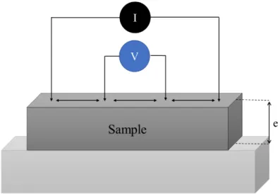
2.9 Four-point probe method
The four-point probe method was used to determine the electrical resistivity of zinc tin nitride thin films. It is a simple device for measuring the resistivity of semiconductor and metallic samples. The principle is based on the electric contact between the surface of the sample and four metallic probes. By passing a current through two outer probes and measuring the voltage through the inner probes the sheet resistance can be measured (fig. 2.10)
42
Figure 2.7 Schematic of the four-point probe method for resistivity measurement.
For a thin film deposited on an insulating substrate, the measurement gives access to the ratio
∆N
O related to the resistivity (ρ in Ω.cm) of materials according to the equation:
𝜌 = Q
RS T 𝑒 N
O (2.2)
Where e is the thickness of the film, V is the voltage measured between the two inner probes and I is the current applied between the two outer probes.
2.10 Hall effect measurements
Hall effect measurements in semiconducting materials can be used to determine accurately conductive type (p or n type), carrier density, electrical resistivity, and the mobility of carriers.
When an electrical current passes through a semiconductor along the x (longitudinal) direction in the presence of a perpendicular magnetic field B along z direction, this induces an electric field 𝐸W along the transverse y direction. The schematic geometry is shown in (fig. 2.11), where the charge accumulation is due to the Lorentz force. The related transverse voltage is called the Hall voltage (𝑉Y), as shown in equation:
𝑉Y = −G.\.]O.[ (2.3)
43
Figure 2.8 Scheme of the Hall effect measurement.
Where 𝐼 is the current across the plat length 𝐵 in the magnetic field, 𝑡 is the thickness of the plate, 𝑒 is the elementary charge and 𝑛 is the charge carrier density of the carrier electrons. In this thesis, the carrier density and the mobility were deduced from Hall measurements in the van der Pauw geometry (Ecopia, HMS-5000).
2.11 UV-visible spectroscopy
To determine the optical properties of the films, different spectroscopy techniques have been used. UV-visible spectroscopy allows the determination of the optical band gap. Soda-lime glass substrate was used for its good transparency (transmittance ≈ 90%) in the visible and in the near infrared range as shown in (fig.2.12).
44
Figure 2.9 Transmission spectrum of the glass substrate.
A Varian Cary 5000 UV-Vis-NIR apparatus was used to determine the optical transmittance measurement. This apparatus works with a double beam and the wavelength can be varied in the range of 200 to 3300 nm. A schematic view of the spectrophotometer is represented in fig. 2.13. A UV-visible light beam is sent to a monochromator and passing with different mirrors. Then, the beam passes through a beam splitter to split the original beam in two beams. One beam passes through a reference compartment while the other is directed to the sample compartment. The two beams are then recovered and are focused onto the detector.
![Figure 1.1 Abundance of elements in the Earth’s crust as funtion of their atomic number[1]](https://thumb-eu.123doks.com/thumbv2/123doknet/15038779.691079/18.892.230.669.110.447/figure-abundance-elements-earth-crust-funtion-atomic-number.webp)
![Figure 1.2 Global capacity of solar photovoltaic by some country and region[3].](https://thumb-eu.123doks.com/thumbv2/123doknet/15038779.691079/19.892.122.779.151.484/figure-global-capacity-solar-photovoltaic-country-region.webp)
![Figure 1.6 The band gaps versus “a” lattice constants for III-nitrides and Zn–IV-nitrides and their alloys.[14]](https://thumb-eu.123doks.com/thumbv2/123doknet/15038779.691079/23.892.243.653.418.740/figure-band-versus-lattice-constants-nitrides-nitrides-alloys.webp)
![Figure 1.13 Theoretical electron pattern for 3 different structures, (a) Electron diffraction pattern simulation for monoclinic structure P2 1 in zone axis [001], (b) Electron diffraction pattern simulation for hexagonal structure P6 3 mc in zone axis [](https://thumb-eu.123doks.com/thumbv2/123doknet/15038779.691079/31.892.136.756.96.667/theoretical-different-structures-diffraction-simulation-monoclinic-diffraction-simulation.webp)