HAL Id: hal-01736041
https://hal.archives-ouvertes.fr/hal-01736041
Submitted on 23 Mar 2018
HAL is a multi-disciplinary open access
archive for the deposit and dissemination of
sci-entific research documents, whether they are
pub-lished or not. The documents may come from
teaching and research institutions in France or
abroad, or from public or private research centers.
L’archive ouverte pluridisciplinaire HAL, est
destinée au dépôt et à la diffusion de documents
scientifiques de niveau recherche, publiés ou non,
émanant des établissements d’enseignement et de
recherche français ou étrangers, des laboratoires
publics ou privés.
Optoelectronic structures with InAlN layers grown by
MOVPE
A.V. Sakharov, W.V. Lundin, E.E. Zavarin, M.A. Sinitsyn, S.O. Usov, A.E.
Nikolaev, S.I. Troshkov, M.A. Yagovkina, D.V. Davydov, Nikolay Cherkashin,
et al.
To cite this version:
A.V. Sakharov, W.V. Lundin, E.E. Zavarin, M.A. Sinitsyn, S.O. Usov, et al.. Optoelectronic structures
with InAlN layers grown by MOVPE. 30th International Conference on the Physics of Semiconductors,
Jul 2010, Séoul, South Korea. pp.107-108, �10.1063/1.3666279�. �hal-01736041�
Optoelectronic structures with InAlN layers grown by MOVPE
A. V. Sakharov, W. V. Lundin, E. E. Zavarin, M. A. Sinitsyn, S. O. Usov, A. E. Nikolaev, S. I. Troshkov, M. A. Yagovkina, D. V. Davydov, N. A. Cherkashin, M. J. Hytch, F. Hue, P. N. Brunkov, and A. F. Tsatsulnikov
Citation: AIP Conference Proceedings 1399, 107 (2011); doi: 10.1063/1.3666279 View online: https://doi.org/10.1063/1.3666279
View Table of Contents: http://aip.scitation.org/toc/apc/1399/1
Optoelectronic structures with InAlN layers grown by
MOVPE
A.V. Sakharov
1*, W.V. Lundin
1, E.E. Zavarin
1, M.A. Sinitsyn
1, S.O. Usov
1,
A.E. Nikolaev
1, S.I. Troshkov
1, M.A. Yagovkina
1, D.V. Davydov
1,
N.A. Cherkashin
2, M.J. Hytch
2, F. Hue
2, P.N. Brunkov
1, and A.F. Tsatsulnikov
11
Ioffe Physico-Technical Institute, Politekhnicheskaya 26, 194021, St-Petersburg, Russia
2
CEMES/CNRS, 29 rue Jeanne Marvig, 31055, Toulouse, France *e-mail [email protected]
Abstract. The results of the some practical applications of InAlN layers in a device hetrostructures grown by MOVPE
is presented. It is shown that use of InAlN allows not only create high-quality DBRs and HEMT structures, but also effectively modify properties of InAlN/GaN/InGaN light-emitting devices.
Keywords: Nitrides, MOVPE, DBR, HEMT. PACS: 81.07.Ta, 81.05.Ea, 85.60.Jb, 81.15.Gh
INTRODUCTION
In spite of the great progress in epitaxy of III-N compounds, most of devices developed during last 20 years were composed of GaN, AlGaN and InGaN layers, which are well technologically developed and investigated. Third ternary alloy in a GaN-AlN-InN system – an InAlN looks very promising but extremely complicated in point of view of synthesis. Use of InAlN in GaN-based optoelectronic structures gives additional degree of freedom, because InAlN depending on composition may be lattice-matched to GaN, tensile or compressively strained. This alloy can be useful for creation of different structures, including HEMT, RC LED and other optoelectronic devices.
EXPERIMENT
Epitaxial structures were grown on (0001) sapphire substrates using two MOVPE systems: standard AIX2000HT with Planetary Reactor and laboratory scale system with horizontal-flow inductively heated single-wafer reactor (strongly re-designed Epiquip VP-50RP). Details of growth can be found in [1].
InAlN/GaN DBRs
Growth of InAlN is a complicated task itself, as growth conditions is a compromise of typical regimes
for InGaN and AlGaN growth. Details of InAlN growth optimisation can be found in [1], below presented some results of InAlN device application. Fine adjustment of growth parameters allows to growth thick enough In0.18Al0.82N layers lattice
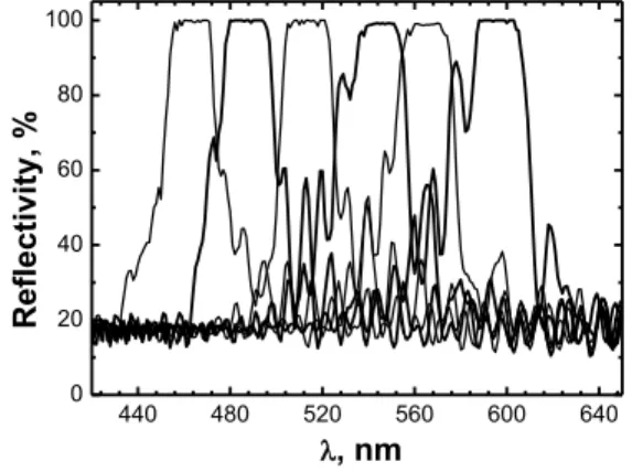
matched to GaN without phase separation and makes possible formation of high-quality DBRs with reflectivity exceeding 99%; Si doping of such structures results in conductive DBR making possible their use as n-type emitters in a RC LEDs with top metallic mirror. 440 480 520 560 600 640 0 20 40 60 80 100 Reflectivity, % O, nm
FIGURE 1. Optical reflectance spectra of InAlN/GaN
57-pair DBRs with different stop-band positions.
Physics of Semiconductors
AIP Conf. Proc. 1399, 107-108 (2011); doi: 10.1063/1.3666279 © 2011 American Institute of Physics 978-0-7354-1002-2/$30.00
InAlN/AlN/GaN HEMTs
Use of InAlN in a 2D electron gas structures shifts the limits for carrier concentration that arise from lattice mismatch in AlGaN/GaN system [3]. For example, concentration can be easily increased from 1.1*1013 cm-2 for GaN/AlN/Al0.3Ga0.7N to
3.1*1013 cm-2 for lattice-matched structure GaN/AlN/In0.18Al0.82N. Moreover, use of InAlN allows
compensating spontaneous polarization by piezoelectric field from compressively strained InAlN. Unfortunately, increase in In composition results in increased alloy scattering and decrease in mobility in spite of decreasing carrier concentration (Table 1).
TABLE 1. Parameters of GaN/AlN/InAlN HEMTs at RT. In Content n, cm-2 *1013 PP, cm2 /Vs 18-19 3.1 667 19-20 2.9 555 20-21 2.8 580 21-22 2.7 520
InAlN/InGaN/GaN LEDs
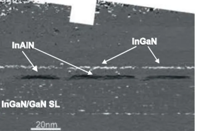
Some specific results were obtained for GaN/InAlN/GaN/InGaN optical structures, were thin (1-18 nm) InAlN layer was grown in regimes close to phase separation. It was observed that growth of GaN/InAlN structure can results in formation of quantum dots with very high density (>2*1011 cm-2 by AFM data). High-resolution transmission electron microscopy (HRTEM) studies of 3 nm-thick InGaN quantum well grown over such bi-layer shows that InGaN grow predominantely over such tenth-nm islands (fig 2) in a strain-control mode.
FIGURE 2. HRTEM image of InGaN QW grown on
InAlN/GaN bi-layer structure.
What is more interesting, these structures exhibit narrow luminescence in a blue spectral region in comparison with 3 nm-thick InGaN QW grown just on GaN layer (see fig.3), indicating strong suppression of phase separation of InGaN inside these 20-30 nm islands. Such structures, combining carrier localization on rather big islands preventing them from nonradiative recombination with “uniform QW”-like spectrum, can be very interesting for applications were narrow gain spectra is necessery, e.g. lasers or electrooptical modulators.
350 400 450 500 550 600
0
1 GaN/InGaN QW
AlInN/GaN/InGaN QW
PL Int., arb. units
O, nm 77K
He-Cd laser
FIGURE 3. PL spectra of InGaN QW grown on GaN
or on InAlN/GaN bi-layer structure.
ACKNOWLEDGMENTS
This work was supported by RFBR grants 08-02-01344-а 10-02-01190-а and Presidium of Russian Academy of Science programme #27.
REFERENCES
1. W.V. Lundin, et al, 13th European Workshop on Metalorganic Vapour Phase Epitaxy, Ulm, Germany, 7-10 June 2009, Booklet of Extended abstracts
2. S.O. Usov, et al Semiconductors 44(7) 981 (2010) 3. W. Colin, J. Debdeep Polarization effects in
semiconductors, Springer, 2007