Abstract—The electrical degradation of InAlN/GaN
high-electron-mobility transistors (HEMTs) for millimeter-wave applications has been examined under simultaneous high VDS,stress and high IDstress electrical stress. Besides a drain current decrease and a positive threshold voltage shift, the creation of an
anomalous source-side gate leakage path has been identified. We attribute this to high electric-field induced trap generation in the AlN layer directly under the gate edge on the source side. The resulting increase in gate leakage further exacerbates the degradation of the gate diode. In addition, we postulate that high power stress leads to significant device self-heating that causes gate sinking and leads to a permanent positive threshold voltage shift and drain current degradation.
Index Terms—InAlN/GaN, trap generation, high electric field,
gate sinking.
I. INTRODUCTION
nAlN/GaN High-Electron-Mobility-Transistors (HEMTs) fabricated on SiC substrates have emerged as promising candidates for high-power millimeter wave applications due to their excellent gate length scaling potential [1]–[5]. With a high spontaneous polarization, a much thinner InAlN barrier layer is required in order to achieve a large enough two-dimensional electron gas (2DEG) density compared with the conventional and more mature AlGaN/GaN HEMT.
I
Recent technology improvements have enabled ultra-scaled InAlN/GaN HEMTs with fT of 400 GHz by minimizing
parasitic effects, as reported in [6]. In addition, InAlN/GaN HEMTs with a low ohmic contact resistance of 0.36 .mm have been realized and reported in [7]. What is more, well rounded InAlN/GaN HEMTs with high drain current (more than 1.2 A/mm), high breakdown voltage (73 V), and
simultaneous high fT (113 GHz) and fmax (230 GHz) have been
reported [8]. All these results demonstrate the potential of InAlN as a barrier material to realize ultra-high-frequency GaN-based HEMTs for power amplifier applications.
Despite the promising properties of this novel heterostructure system, in nanometer-scale InAlN/GaN HEMTs, the use of a very thin barrier layer brings gate
Manuscript received _________________. This research is funded by National Reconnaissance Office contract number DII NRO000-13C0309.
Y. Wu and J. A. del Alamo are with Microsystems Technology
Laboratories, Massachusetts Institute of Technology, Cambridge, MA 02139, USA (e-mail: [email protected]; [email protected]).
W. A. Sasangka is with Singapore-MIT Alliance for Research and Technology, 1 CREATE Way, #10-01 CREATE Tower Singapore 138602.
leakage current and reliability concerns to the fore. In this regard, the literature is very sparse.
It has been reported that in AlGaN/GaN HEMTs, under extended OFF-state stress, time-dependent defect generation in the AlGaN barrier layer can result in an increase of gate leakage even if the stress voltage is not very high [9]. In addition, recently, under forward gate stress, similar time-dependent defect generation in the gate stack of p-GaN gate AlGaN/GaN HEMTs has been observed [10]. However, so far to our knowledge, there are no studies that have focused on the degradation mechanisms related to the gate region of InAlN/GaN HEMTs under high-power conditions. Developing an understanding of these issues is the motivation for our work.
This manuscript presents a study of reliability of InAlN/GaN HEMTs with emphasis on high-power stress conditions. We have observed the creation of an anomalous source-side gate leakage path. This is in contrast to the commonly observed drain-side degradation in GaN HEMTs [11]–[13]. Temperature-dependent studies as well as positive gate stress experiments have allowed us to separately identify two permanent degradation mechanisms associated with this: gate leakage current increase and gate sinking. Our research should be instrumental in realizing the potential of InAlN/GaN HEMTs in high frequency applications.
II. DEVICES AND EXPERIMENTS The devices studied here are industrially prototyped InAlN/GaN HEMTs with LG = 40 nm fabricated on a SiC
wafer [14]. Enhancement-mode operation is achieved through gate recessing of the entire InAlN layer leaving only a 1 nm AlN barrier between the channel and the gate metal.
Our previous work suggests that these devices experience the most severe degradation under ON-state stress [14]. In this regard, for this study, we have carried out accelerated ON-state high-power stress experiments under simultaneous high VDS,stress and IDstress conditions which emulate the quiescent bias
point in a power amplifier application. A typical example is shown in Fig. 1 that graphs (a) output (at VGS = 2 V) and (b)
transfer (at VDS = 4 V) I-V characteristics of a device before
and after constant stress at VDS,stress = 25 V and IDstress = 400
mA/mm for 5 minutes at room temperature (RT) [15]. The estimated junction temperature, according to the thermal model provided by our industrial collaborator, is Tj = 136 °C.
VGS,stress was around 1.5 V but was allowed to change during
the experiment in order to maintain the desired IDstress level.
The characteristics of Fig. 1 have been obtained after thermal
Anomalous Source-side Degradation of
InAlN/GaN HEMTs under High-Power
Electrical Stress
detrapping and therefore reflect permanent device degradation. Detailed information about our detrapping methodology can be found in [14].
Besides a significant decrease in drain current and a positive VT shift, OFF-state drain current markedly increased after
stress. Not shown are RD after stress which increased by a
noticeable amount. RS, while also increased after stress, is
much less affected if compared with RD. RD and RS are
measured by the gate injection method with IGinj = 20 mA/mm
[16].
Similar experiments were also carried out at a low substrate temperature with the goal of identifying the role of
temperature in the observed degradation. Fig. 2 shows (a) output and (b) transfer characteristics in such an experiment before and after constant stress at VDS,stress = 25 V and IDstress =
500 mA/mm with Tchuck = -50 °C (estimated Tj = 85 °C).
VGS,stress was at around 1.4 V during the experiment and varied
in order to maintain the designed IDstress level. This lower
required VGS,stress level to achieve high IDstress, with respect to the
previous experiment reflects the negative shift of VT that takes
place as the temperature is reduced. The device in Fig. 2 showed some drain current decrease in saturation regime and a small positive VT shift, but much less than in the RT
temperature experiment even though the stress current level is higher. The OFF-state drain current also increased due to stress. In summary, low-T stress results in smaller ID
degradation. RD and RS both increased after stress with RD
exhibiting larger change compared with RS, similar to what
was observed in the RT experiment.
To complement this picture, Fig. 3 shows the evolution of the RT gate current for both experiments. The measurements are also performed after thermal detrapping and reflect permanent degradation. Both devices exhibit significant gate leakage increase in the reverse and low forward gate bias regimes. This indicates that a lower stress temperature only marginally reduces gate current degradation under high-power stress. This is different from the degradation signature of ID.
These and other experiments suggest two different degradation mechanisms for gate current and drain current where ID
degradation is strongly thermally enhanced and IG degradation
is less affected by temperature.
III. SOURCE-SIDE GATE LEAKAGE PATH To better understand the origin of the gate leakage current increase after high-power stress, we have carried out three-terminal current measurements and extracted the current
distribution through the source and drain terminals as a function of gate voltage.
Figure 1. (a) Output and (b) transfer characteristics of a device before and after constant stress at VDSstress = 25 V and IDstress = 400 mA/mm at
RT. The device was thermally detrapped before and after stress. A large ID decrease and a positive VT shift are observed after stress. Also, a
significant off-state drain leakage current increase is induced by stress.
Figure 3. RT IG-VGS plots before and after stress of the device in (a) Fig.
1 and (b) Fig. 2. The device was thermally detrapped before and after stress. IG increased significantly in both experiments.
Figure 2. (a) Output and (b) transfer characteristics of a device before and after constant stress at VDS,stress = 25 V and IDstress = 500 mA/mm at
-50oC. The device was thermally detrapped before and after stress. I D
decrease and positive VT shift as well as drain leakage current increase
are observed after stress. Compared with the RT experiment in Fig. 1, the
-6 -4 -2 0 2 10-13 10-11 10-9 10-7 10-5 10-3 10-1 ID, after stress
|I|
(
A
)
V
GS(V)
ID, before IG, before IS, before ID, after IG, after IS, after IG, IS after stressFigure 4. IG-VGS characteristics (measured at 25 °C) at VDS=0 before
(solid lines) and after (dashed lines) constant stress at VDS,stress = 25 V and
IDstress = 400 mA/mm (same experiment as in Figs. 1 and 3(a)). IS and ID
are also indicated. After stress, IG and IS increase by several orders of
Fig. 4 shows the three terminal currents before and after stress (thermally detrapped) for the RT stress experiment
corresponding to Fig. 1. Similar to what Fig. 3(a) suggests, IG
after stress increases by several orders of magnitude. Surprisingly, IS closely follows IG whereas ID increases much
less. This suggests that the gate current increase takes place through a leakage path created between the gate and the source. A similar source-side leakage increase is also observed in the low T experiment of Fig. 2 (Fig. 5). This unique degradation signature of source-side damage of the gate diode is uncommon in conventional AlGaN/GaN HEMTs [17] as well as InAlN/GaN HEMTs after ON-state stress [18].
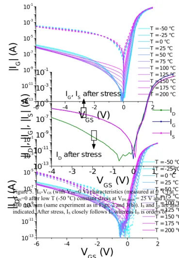
In order to understand the origin of the observed source side degradation, we have studied the temperature dependence of the three terminal currents before and after stress. For the RT stress experiment, Fig. 6 (a) and (b) shows IG and ID,
respectively, for Tchuck from -50 °C to 200 °C in 25 °C steps
before (solid lines) and after (dashed lines) stress. IS behaves
similarly to IG and is not shown here.
From Fig. 6 (a), before stress, the temperature dependence of IG can be separated into three regimes: regime I with VGS >
0 V, regime II with low reverse gate bias (~ -1 V < VGS < 0 V)
and regime III with high reverse gate bias (VGS < -2 V). In
-6 -4 -2 0 2 10-13 10-11 10-9 10-7 10-5 10-3 10-1
|I
G| (
A
)
V
GS(V)
T = -50 °C T = -25 °C T = 0 °C T = 25 °C T = 50 °C T = 75 °C T = 100 °C T = 125 °C T = 150 °C T = 175 °C T = 200 °C -6 -4 -2 0 2 10-13 10-11 10-9 10-7 10-5 10-3 10-1|I
D| (
A
)
V
GS(V)
T = -50 °C T = -25 °C T = 0 °C T = 25 °C T = 50 °C T = 75 °C T = 100 °C T = 125 °C T = 150 °C T = 175 °C T = 200 °CFigure 6. (a) IG-VGS (with VDS=0 V) and (b) ID-VGS (with VDS=0 V) before
(solid lines) and after (dashed lines) constant stress at VDS,stress = 25 V and
IDstress = 400 mA/mm (same experiment as in Figs. 1, 3(a) and 4). The I-V
sweeps were conducted at Tchuck from -50 °C to 200 °C in 25 °C steps.
-4 -3 -2 -1 0 1 2 10-13 10-11 10-9 10-7 10-5 10-3 10-1 ID after stress
|I
D|,
|I
G|,
|I
S| (
A
)
V
GS(V)
ID IG IS IG, IS after stressFigure 5. IG-VGS (with VDS=0 V)characteristics (measured at 0 °C) at
VDS=0 after low T (-50 °C) constant stress at VDS,stress = 25 V and IDstress =
500 mA/mm (same experiment as in Figs. 2 and 3(b)). IS and ID are also
regimes I and II in the virgin device, |IG| exhibits a positive
temperature dependence, suggesting a Thermionic or Thermionic Field Emission dominated charge transport mechanism for the entire gate diode on both the source and drain sides. In regime III, on the other hand, |IG| exhibits a
negative temperature dependence. This could be due to drift-limited current transport in the access regions of the device.
Stress has a significant impact in the T dependence of the currents in all three regimes for IG and IS, much less so for ID.
As shown by the dashed lines in Fig. 6 (a), a significantly reduced temperature dependence is observed in all three regimes for IG and IS, indicating a dominance of electron
tunneling. This posits a possible explanation to the source-side degradation: the formation of defects in the AlN layer on the source side, leading to significantly increased trap-assisted conduction mechanisms, such as trap-assisted-tunneling or Poole-Frenkel emission. The drain side of the gate diode is less affected due to the reverse bias prevalent there under high power conditions. ID, as a result, more or less retains its
temperature dependence (Figure 6 b). Similar results have
been observed in the sample subjected to low-temperature stress.
IV. DISCUSSION
Considering these and similar experiments together, a hypothesis for the observed degradation phenomena emerges. Under high VDS,stress and IDstress, the gate-source diode is strongly
forward biased and there is significant gate current. For the RT experiment shown in Fig. 1, IGstress increased from about 10
mA/mm to 50 mA/mm and similarly for the low T experiment shown in Fig. 2, IGstress increased from about 20 mA/mm to 45
mA/mm. In addition, there is high power dissipation and self-heating. The combination of high gate current, high
temperature and high forward gate voltage, and therefore strong electric field across the 1 nm AlN barrier on the source side, generates defects in the AlN. Similar defect formation has been observed in the AlGaN/GaN system under strong reverse bias conditions [9] and also in AlGaN/GaN devices with p-GaN gate under forward bias stress [10]. On the drain side of the gate, the field across the AlN barrier is reversed and is most likely smaller due to the appearance of a
depletion region in the access region next to it. This results in much less degradation compared with the source side.
Separately from this, local device self-heating due to significantly increased gate leakage current on top of the high power stress (
V
DS stress,
I
Dstress) produces gate sinking and a positive VT shift [19]–[21]. The decreased saturation draincurrent, IDmax is likely due to the VT positive shift. The RD
increase is also consistent with the positive VT shift, since
after stress, the increased resistance associated with the intrinsic channel starts to play a non-negligible role in the extraction of RD through the current injection method.
Our defect generation hypothesis suggests that a similar degradation should take place under forward gate bias stress under VDS=0 V conditions if the electric field and temperature
are high enough, except that in this case, the degradation should occur in a symmetric way.
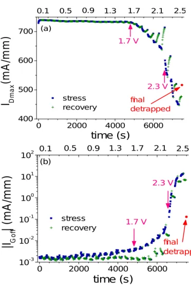
To verify this, we conducted a step-stress-recovery experiment at RT with source and drain grounded and positive VGS,stress increasing from 0.1 V to 2.5 V in 0.1 V steps.
The stress time during each step was 5 minutes. Fig. 7 shows the evolution of IDmax and IGoff with time during stress.
We observe that IDmax reduction (Fig. 7 (a)) and IGoff
increase (Fig. 7 b) start at around VGS,stress=1.7 V. This
corresponds to the onset of defect formation in the AlN layer. As stress continues, a significant acceleration of IGoff
degradation occurs when VGS,stress exceeds ~ 2.3 V. Also, fast
IDmax decrease and RD and RS increase (not shown) take place
at the same time, indicating a second degradation mechanism kicking in. 0 2000 4000 6000 400 500 600 700 (a) 2.3 V 2.5 2.1 1.7 1.3 0.9 0.5 stress recovery
I
Dm ax(
m
A
/m
m
)
time (s)
final detrapped 0.1 1.7 V 0 2000 4000 6000 10-3 10-2 10-1 100 101 102 2.5 final detrapped stress recovery|I
Gof| (
m
A
/m
m
)
time (s)
2.1 0.1 0.5 0.9 1.3 1.7 1.7 V 2.3 V (b)Figure 7. Degradation of (a) IDmax (at VGS = 2 V, VDS = 4 V) and (b) |IGoff|
(at VGS = -2 V, VDS = 0.1 V) as a function of stress time in a
step-stress-recovery experiment with VGstress>0 and VDS=0. IDmax and IGoff start to
degrade at VGS,stress around 1.8 V. Enhanced degradation takes place for
VGstress beyond 2 V, indicating defect formation in the AlN layer. Final
detrapped values are also shown as red dots indicating a permanent decrease in drain current and a permanent increase in gate leakage current.
To make the overall picture clearer, the time evolution of the gate current during stress is shown in Fig. 8. Before VGS,stress reaches 2.3 V, for constant stress, IGstress decreases with
time which is the typical signature of electron trapping. When VGS,stress exceeds 2.3 V, at constant stress, the IGstress behavior
changes significantly and starts to increase with time. This marks the onset of a second degradation mechanism. The signature of this mechanism is enhanced IGoff leakage, IDmax
decrease, as well as RD and RS increase (not shown). This
degradation pattern is similar to that observed under prolonged high-power stress discussed previously and is believed to be related to device self-heating induced Schottky gate
degradation, possibly gate sinking.
-6 -4 -2 0 2 10-13 10-11 10-9 10-7 10-5 10-3 10-1
|I|
(
A
)
V
GS(V)
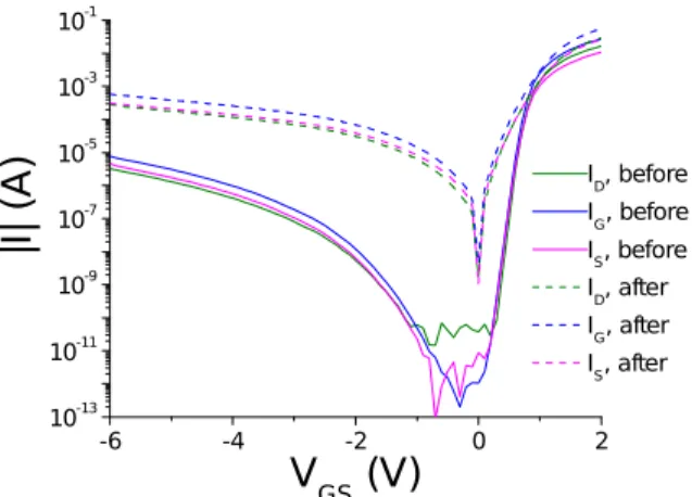
ID, before IG, before IS, before ID, after IG, after IS, afterFigure 9. IG-VGS characteristics at VDS=0 before (solid lines) and after
(dashed lines) positive VGS step-stress-recovery experiment of Fig. 7 and
8 with VDS=0. IS and ID are also indicated. After stress, IG roughly splits
in half between ID and IS indicating degradation of both source and drain
0 2000 4000 6000 10-7 10-5 10-3 10-1 101 103 (a) 2.5 IGst re ss ( m A /m m ) tstress (s) 2.1 0.1 0.5 0.9 1.3 1.7 VGS,stress (V) 4800 5600 6400 7200 102 103 2.5 (b) IGst re ss ( m A /m m ) tstress (s) VGS,stress (V) 1.7 1.9 2.1 2.3 VGS,stress = 2.3 V
Figure 8. (a) Time evolution of IGstress (at VG = VGS,stress, VDS,stress = 0 V) as
VGS,stress increases from 0.1 to 2.5 V in 0.1 V steps. (b) Zoomed-in view of
(a) for VGS,stress ranging from 1.3 to 2.5 V. Before VGS,stress reaches 2.3 V,
IGStress decreases with time for each VGS,stress level, possibly due to electron
trapping. As VGS,stress exceeds 2.3 V, IGstress exhibits an observable increase
Unlike in the high-power stress experiments before, the three-terminal current measurements for this device show that the permanent increase in IG after stress splits roughly in half
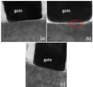
through the source and drain (Fig. 9). This is just as expected. In order to verify the gate sinking hypothesis, we carried out cross-sectional structural analysis with TEM on both virgin devices and stressed devices. Fig. 10 shows HR-TEM images of the intrinsic gate regions of three devices: Fig. 10 (a) is a virgin device, (b) is the device stressed under high-VDS,stress
-high-IDstress condition discussed previously (Fig. 1), and (c) is a
device stressed under positive step-VGS condition with VGS,stress
increasing from 0 V to 2.5 V (VDS,stress = 0 V), similar to the
experiment shown in Figs. 7 and 8 except that the stress temperature was Tstress = 150 °C instead of RT. This device
exhibits a degradation pattern of the second degradation mechanism tentatively attributed to gate sinking. That is, a significantly increased IGoff, a decreased IDmax, as well as
increased RD and RS. Fig. 11 shows the transfer (a) and gate
current (b) characteristics of this device before and after stress. Permanent degradation for this device is more severe than the device stressed under high-VDS,stress-high-IDstress condition at RT
(Fig. 1).
Figure 10. HRTEM cross-sectional image of intrinsic gate region of three devices: (a) virgin device; (b) device stressed under high-VDS,stress
-high-IDstress condition as in Fig. 1; (c) device stressed under high T (150
Interestingly, for both the virgin device (a) and the device stressed under high-VDS,stress-high-IDstress condition (b), there is a
light region between the gate metal and the underlying semiconductor layer. From electron energy loss spectroscopy (EELS) analysis, we have confirmed that the light region corresponds to some oxide species. This is likely due to the oxidation of AlN interlayer during the gate recess step and should then exist in all devices. We have verified this in two other virgin samples. Similar thin native oxide layers at the semiconductor/metal interface has been reported also in AlGaN/GaN HEMTs in the past [22].
For the device stressed under high T and harsh VGS,stress
condition with VDS,stress=0 V, Fig. 10 (c) shows that the oxide
layer seems to have been almost completely consumed over most of the gate area. This is similar to what has previously been observed in AlGaN/GaN HEMTs after high electric field stress at high temperature [21], [22]. This most likely is the gate sinking mechanism postulated above. The reduction of the interfacial oxide would shift VT positive and result in a
large increase in IG. This positive VT shift will then result in
decreased IDmax due to a reduction in gate overdrive. The RD
and RS increases are also most likely associated with the VT
shift since the measured resistance through the gate-current injection technique includes half of the channel resistance. In an enhancement-mode device, this can increase significantly as VT shifts positive.
Figure 10 (b), for the sample stressed under high-power conditions, shows partial consumption of the light oxide layer in the region highlighted by the red circle. EELS line scans at three locations across the device gate verified that in the red circled area the interfacial oxide layer is the thinnest. This incomplete consumption of native oxide layer, as compared with the more complete dissolution in Fig. 10 (c), is consistent with the lower degree of overall permanent electrical
degradation observed in this device.
V. CONCLUSIONS
In summary, we have identified an anomalous source-side gate degradation in InAlN/GaN HEMTs stressed under simultaneous high VDS and high ID conditions. We have found
that a strong positive bias on the gate coupled with self-heating leads to a significant increase in gate leakage current that flows through the source side of the device. We attribute this to defect formation in the AlN barrier driven by high electric field and high temperature, coupled with gate sinking. Our study should be instrumental in aiding the development of reliable scaled InAlN/GaN HEMTs.
VI. ACKNOWLEDGMENTS
We acknowledge fruitful discussion with Jose Jimenez of Qorvo. We also thank Qorvo for providing the devices used for this study.
REFERENCES
[1] F. Medjdoub, M. Alomari, J.-F. Carlin, M. Gonschorek, E. Feltin, M. A. Py, N. Grandjean, and E. Kohn, "Barrier-Layer Scaling of InAlN/GaN HEMTs," IEEE Electron Dev. Lett., vol. 29, no. 5, pp. 422-425, May 2008.
[2] H. Behmenburg, L. Rahimzadeh Khoshroo, M. Eichelkamp, C. Mauder, M. Fieger, N. Ketteniss, J. Woitok, D.
Wamwang, M. Wuttig, S. Estevez Hernandez, T. Schapers, M. Heuken, A. Vescan, H. Kalisch, and R. H. Jansen, "Influence of barrier thickness on AlInN/AlN/GaN heterostructures and device properties," Phys. Status Solidi C, vol. 6, no. S2, pp. 1041-1044, Jan. 2009.
[3] A. Crespo, M. M. Bellot, K. D. Chabak, J. K. Gillespie, G. H. Jessen, V. Miller, M. Trejo, G. D. Via, D. E. Walker, Jr. B. W. Winningham, H. E. Smith, T. A. Cooper, X. Gao, and S. Guo, "High-Power Ka-Band Performance of AlInN/GaN HEMT With 9.8-nm-Thin Barrier," IEEE Electron Dev. Lett., vol. 31, no. 1, pp. 2-4, Jan. 2010.
[4] Md. Tanvir Hasan, H. Tokuda, and M. Kuzuhara, "Surface barrier height lowering at above 540 K in AlInN/AlN/GaN heterostructures," Appl. Phys. Lett., vol. 99, no. 132102, pp. 1-3, Sept. 2011.
[5] H. Pardeshi, G. Raj, S. Pati, N. Mohankumar, and C. K. Sarkar, "Influence of barrier thickness on AlInN/GaN underlap DG MOSFET device performance," Superlattices
and Microstruct., vol. 60, pp. 47-59, April 2013.
[6] Y. Yue, Z. Hu, J. Guo, B. Sensale-Rodriguez, G. Li, R. Wang, F. Faria, B. Song, X. Gao, S. Guo, T. Kosel, G. Snider, P. Fay, D. Jena, and H. G. Xing, "Ultrascaled InAlN/GaN High Electron Mobility Transistors with Cutof Frequency of 400 GHz," Jpn. J. Appl. Phys., vol. 52, no. 08JN14, pp. 1-2, May 2013.
[7] S. Arulkumaran, G. I. Ng, K. Ranjan, C. M. M. Kumar, S. C. Foo, K. S. Ang, S. Vicknesh, S. B. Dolmanan, T. Bhat, and S. Tripathy, "Record-low contact resistance for
InAlN/AlN/GaN high electron mobility transistors on Si with non-gold metal," Jpn. J. Appl. Phys., vol. 54, no. 04DF12, pp. 1-5, March 2015.
[8] K. Joshin, K. Makiyama, S. Ozaki, T. Ohki, N. Okamato, Y. Niida, M. Sato, S. Masuda, and K. Watanabe, "Millimeter-Wave GaN HEMT for Power Amplifier Applications," IEICE Trans. Electron., vol. e97-c., no. 10, pp. 923-929, Oct. 2014.
[9] D. Marcon, G. Meneghesso, T-L Wu, S. Stofels, M. Meneghini, E. Zanoni, and S. Decoutere, "Reliability Analysis of Permanent Degradations on AlGaN/GaN HEMTs," IEEE Trans. Electron Dev., vol. 60, no. 10, pp. 3132-3141, Oct. 2013.
[10] I. Rossetto, M. Meneghini, O. Hilt, E. Bahat-Treidel, C. D. Santi, S. Dalcanale, J. Wuerfl, and E. Zanoni, "Time-Dependent Failure of GaN-on-Si Power HEMTs With p-GaN Gate," IEEE Trans. Electron. Dev., vol. 63, no. 6, pp. 2334-2339, June 2016. -2 -1 0 1 2 10-3 10-2 10-1 100 101 102 103 -2 -1 0 1 2 10-9 10-7 10-5 10-3 10-1 101 103 VDS = 4 V ID ( m A /m m ) VGS (V) before stress after stress (a) (b) VDS = 0.1 V |IG | ( m A /m m ) VGS (V) before stress after stress
Figure 11. (a) Transfer and (b) gate current characteristics of device before and after high T positive step-VGS stress. Measurements after the
device was thermally detrapped. IDmax decrease and IGoff increase are
observed after stress. The subthreshold characteristics are severely degraded. Excessive gate leakage current after stress makes the threshold voltage extraction not accurate.
[11] J. Joh and J. A. del Alamo, "Mechanisms for Electrical Degradation of GaN High-Electron Mobility Transistors," 2006 International Electron Devices Meeting, San Francisco, CA, 2006, pp. 1-4., Dec. 2006.
[12] J. Joh and J. A. del Alamo, "Critical voltage for electrical degradation of GaN high-electron mobility transistors," IEEE Electron Device Lett., vol. 29, no. 4, pp. 287-289, Apr. 2008.
[13] J. A. del Alamo and J. Joh, "GaN HEMT reliability," Microelectron. Reliab., vol. 49, no. 5, pp. 1200-1206, July 2009.
[14] Y. Wu and J. A. del Alamo, "Electrical Degradation of InAlN/GaN HEMTs Operating Under ON Conditions," IEEE Trans. Electron Dev., vol. 63, no. 9, pp. 3487-3492, Sept. 2016.
[15] Y. Wu and J. A. del Alamo, "Anomalous Source-Side Degradation of InAlN/GaN HEMTs under ON-State Stress," International Workshop on Nitride Semiconductors (IWN), Orlando, FL, October 2-7, 2016.
[16] D. R. Greenberg and J. A. del Alamo, "Nonlinear Source and Drain Resistance in Recessed-Gate Heterostructure Field-Efect Transistors," IEEE Trans. Electron. Dev., vol. 43, no. 8, pp. 1304-1306, Aug. 1996.
[17] M. Meneghini, G. Meneghesso, and E. Zanoni, "Analysis of the Reliability of AlGaN/GaN HEMTs Submitted to On-State Stress Based on Electroluminescence
Investigation," IEEE Trans. Dev. Mater. Reliab., vol. 13, no. 2, pp. 357-361, June 2013.
[18] C. Y. Zhu, M. Wu, C. Kayis, F. Zhang, X. Li, R. A. Ferreyra, A. Matulionis, V. Avrutin, U. Ozgur, and H. Morkoc, "Degradation and phase noise of InAlN/AlN/GaN
heterojunction field efect transistors Implications for hot electron/phonon efects," Appl. Phys. Letts., vol. 101, no. 103502, pp. 1-4, Sept. 2012.
[19] D. J. Cheney, E. A. Douglas, L. Liu, C. F. Lo, Y. Y. Xi, B. P. Gila, F. Ren. D. Horton, M. E. Law, D. J. Smith, and S. J. Pearton, "Reliability studies of AlGaN/GaN high electron mobility transistors," Semicond. Sci. Technol., vol. 28, no. 074019, pp. 1-12, June 2013.
[20] E. A. Douglas, C. Y. Chang, D. J. Cheney, B. P. Gila, C. F. Lo, L. Lu, R. Holzworth, P. Whiting, K. Jones, G. D. Via, J. Kim, S. Jang, F. Ren, and S. j. Pearton, "AlGaN/GaN High Electron Mobility Transistor degradation under on-and of-state stress," Microelectron. Reliab., vol. 51, pp. 207-211, Feb. 2011.
[21] H. Jung, R. Behtash, J. R. Thorpe, K. Riepe, F. Bourgeois, H. Blanck, A. Chuvilin, and U. Kaiser, "Reliability behavior of GaN HEMTs related to Au difusion at the Schottky interface," Phys. Stat. Solidi C, vol. 6, no. S2, pp. S976-979, March 2009.
[22] C. Ostermaier, G. Pozzovivo, B. Basnar, W. Schrenk, M. Schmid, L. Toth, B. Pecz, J.-F. Carlin, M. Gonschorek, N. Grandjean, G. Strasser, D. Pogany, and J. Kuzmik, "Metal-related gate sinking due to interfacial oxygen layer in Ir/InAlN high electron mobility transistors," Appl. Phys. Lett., vol. 96, no. 26315, pp. 1-3, July 2010.
Yufei Wu received the B.S. and M.S. degrees from The
Pennsylvania State University and the Massachusetts Institute of Technology, U.S., in 2012 and 2014, both in electrical engineering. She is currently working towards her Ph.D. degree in Electrical Engineering at the Massachusetts Institute of Technology. Her research topics include modelling and
testing reliability of GaN FETs.
W. A. Sasangkareceived his
Ph.D in advanced materials science for micro- and nano-system from Nanyang Technological University in 2012. Since then, he joined Singapore-MIT Alliance for Research and Technology (SMART) as a research scientist. He has broad research interests such as GaN reliability, nanowires growth, thin film interdiffusion, and crystal defect characterization. He is an active member of organizing committee in International Symposium on the Physical and Failure Analysis of Integrated Circuits (IPFA).
Jesus A. del Alamo (S'79, M'85, SM'92, FM'06) received the
Telecommunications Engineer degree from the Polytechnic University of Madrid, Madrid, Spain, in 1980, and the M.S. and Ph.D. degrees in electrical engineering from Stanford University, Stanford, CA, USA, in 1983 and 1985,
respectively. He has been with the Massachusetts Institute of Technology, Cambridge, MA, USA, since 1988, where he is currently a Donner Professor. At the present, his research interests are microelectronics technologies for