HAL Id: hal-01740323
https://hal.archives-ouvertes.fr/hal-01740323
Submitted on 21 Mar 2018
HAL is a multi-disciplinary open access
archive for the deposit and dissemination of
sci-entific research documents, whether they are
pub-lished or not. The documents may come from
teaching and research institutions in France or
abroad, or from public or private research centers.
L’archive ouverte pluridisciplinaire HAL, est
destinée au dépôt et à la diffusion de documents
scientifiques de niveau recherche, publiés ou non,
émanant des établissements d’enseignement et de
recherche français ou étrangers, des laboratoires
publics ou privés.
Static strain tuning of quantum dots embedded in a
photonic wire
D. Tumanov, N. Vaish, H.-A. Nguyen, Y. Curé, J.-M Gérard, J. Claudon, F.
Donatini, J.-P. Poizat
To cite this version:
D. Tumanov, N. Vaish, H.-A. Nguyen, Y. Curé, J.-M Gérard, et al.. Static strain tuning of quantum
dots embedded in a photonic wire. Applied Physics Letters, American Institute of Physics, 2018, 112
(12), pp.123102. �10.1063/1.5025313�. �hal-01740323�
D. Tumanov1,2, N. Vaish1,2, H.A. Nguyen1,2, Y. Curé3, J.-M. Gérard3, J. Claudon3, F. Donatini1, and J.-Ph. Poizat1,2,∗
1
Univ. Grenoble Alpes, CNRS, Grenoble INP, Institut NEEL, F-38000 Grenoble, France
2
Univ. Grenoble Alpes, CNRS, Grenoble INP, Institut NEEL, "Nanophysique et semiconducteurs" group, 38000 Grenoble, France
3
Univ. Grenoble Alpes, CEA, INAC, PHELIQS,
"Nanophysique et semiconducteurs" group, F-38000 Grenoble, France * Corresponding author : [email protected]
(Dated: March 6, 2018)
We use strain to statically tune the semiconductor band gap of individual InAs quantum dots (QDs) embedded in a GaAs photonic wire featuring very efficient single photon collection efficiency. Thanks to the geometry of the structure, we are able to shift the QD excitonic transition by more than 20 meV by using nano-manipulators to apply the stress. Moreover, owing to the strong trans-verse strain gradient generated in the structure, we can relatively tune two QDs located in the wire waveguide and bring them in resonance, opening the way to the observation of collective effects such as superradiance.
Epitaxial semiconductor quantum dots (QDs) embed-ded in nanophotonic structures are very efficient single photon sources (see [1–3] and [4] for a review). How-ever their use in quantum information protocols involving more than two sources has been hindered by the disper-sion in energy of different QDs. This disperdisper-sion is due to their intrinsically random self-assembly fabrication pro-cess [5], so that two QDs are never alike. QD energy tun-ing can be achieved ustun-ing temperature [6], electric field [7–9], or material strain [10–14]. Temperature tuning is limited to fine tuning. Electrical control is also suitable for fine tuning and can reach shifts up to 25 meV [9]. Strain tuning can be used for fine tuning [10, 11, 13, 14] (see [15] for a review) and, as temperature and electrical tuning, can enable two-photon interferences with two dif-ferent QDs [6, 8, 11]. Interestingly, it offers the additional possibility to generate ultra-large shifts up to 500 meV as demonstrated by Wu et al [12] using a diamond anvil cell. Such cells are however limited to bulk systems and are unsuitable to QDs embedded in photonic environments. Fine strain tuning is usually realized by bonding the bulk QD structure on piezoelectric actuators [10–12, 14, 15], imposing limitations on the structure geometry. Remark-ably, Kremer et al [13] managed to achieve up to 1.2 meV strain tuning for a QD embedded in a nanowire antenna using this bonding technique.
In this paper, we demonstrate large static strain tuning (up to 25 meV) of QDs embedded in a photonic waveg-uide allowing efficient light extraction [1]. Four years ago, these photonic structures were used by some of us as mechanical oscillator to demonstrate strain-mediated op-tomechanical coupling [16] (see also [17]). In the present work, the strain is produced statically using a nanoma-nipulator enabling the realization of bright and broadly tunable quantum light sources. In addition, since the generated strain field features a very large gradient across the wire diameter [18], our method allows us to bring in mutual resonance two QDs contained in a waveguide and opens interesting perspective for the observation of
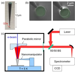
Figure 1. (a) Tilted scanning electron microscope (SEM) view of the GaAs photonic tapered waveguide from sample S1. The QDs (red triangle) are located 110 nm above the basis. The top facet is covered by an anti-reflection coating (false, green color). (b) SEM top view showing the top facet of a waveguide and the tip of the nanomanipulator. Between the left and right image, the tip has moved and pushed the top of the waveguide by 1 µm. (c) Experimental set-up based on a modified cathodoluminescence set-up: a laser excites the QDs photoluminescence and we use SEM imaging to monitor the position of the tip with respect to the top facet.
collective spontaneous emission effects such as superra-diance [19].
Our system is based on the GaAs tapered waveguide shown in Fig.1(a) and described in detail in [1]. The waveguide from sample S1 that we have used for the first experiment (see Fig.2) is 12 µm high. The top diame-ter has been measured to 1.69 µm, and the bottom di-ameter to 350 nm. Self-assembled InAs QDs (around 10) are located at random lateral positions in a plane at
2
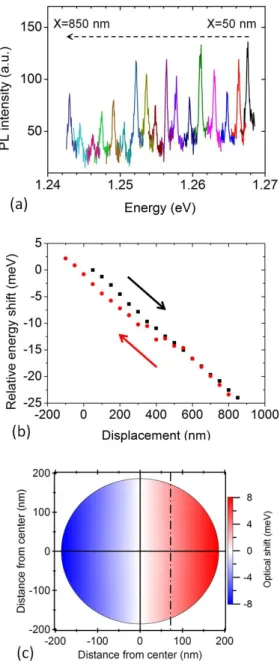
Figure 2. Energy shift as a function of the displacement X of nanomanipulator tip obtained from a QD embedded in the waveguide from sample S1. (a) Photoluminescence spectrum of a single QD for varying nanomanipulator positions X. The right most peak corresponds to X = 50 nm and the left most to X = 850 nm. The increment between two consecutive peaks is 50 nm. (b) Relative energy shift as a function of the displacement of nanomanipulator tip corresponding to the data shown in (a). The black square are for increasing dis-placement, and the red circles correspond to the way back. The slight kink on the way back is attributed to the slippage of the tip. (c) Map of the calculated energy shift caused by the strain gradient across the QD plane for a top facet dis-placement of 100 nm along the horizontal axis. The slope of 31 µeV/nm of (b) corresponds to a QD located on the dash-dotted line at 70 nm from the zero strain line.
110 nm above the basis of the structure, which stands on a planar gold mirror to redirect all the light to the top. This photonic structure has been designed for effi-cient collection of the single photons emitted by the QDs [1] as well as for the efficient optical addressing of the QD [20, 21]. This inverted cone geometry also features a very strong optomechanical coupling: the mechanical displacement of the top facet induces a large strain in the lower part of the structure affecting the energy of the fun-damental excitonic QD transition [16]. In [16], the top facet motion was caused by the mechanical oscillation of the fundamental flexural mode. In the present work, the displacement is induced statically by a tungsten tip mounted on a nanomanipulator pushing the structure top (see Fig.1(b),(c)). We then excite the QD photolumines-cence (PL) to determine the effect of this static stress on the excitonic line energy.
To perform these experiments, we have adapted a cathodoluminescence set-up to benefit from a scanning electron microscope (SEM) operating at cryogenic tem-perature and equipped with a window for optical access (see Fig.1(c)). This allowed us to use SEM imaging to monitor the relative position of the nanomanipulator tip with respect to the waveguide (see Fig.1(b)) while ex-ploiting the optical access to carry out PL experiments at a temperature T = 5 K. The PL is excited by a con-tinuous laser tuned to λ = 830 nm, below the energy band gap of GaAs. The laser beam is focused on the device with an aluminum parabolic mirror and generates charge carriers in the QDs wetting layer. The QDs PL is collected with the same mirror, and is sent to a grating spectrometer equipped with a CCD camera for spectral analysis. The alignment of the optical part of the setup is relatively delicate. The device is first aligned on the focal point of the parabola in cathodoluminescence mode (luminescence excitation by the e-beam). The laser beam is then shaped and aligned to be mode-matched with the cathodoluminescence beam. In order to insure a sufficient signal on noise ratio in our in-situ SEM PL experiment, the input slit of the spectrometer has to be opened, lim-iting the spectral resolution to about 300 µeV as can be noticed in the experimental spectra below. With a high-resolution PL set-up, the line-widths of QDs embedded in these waveguides are typically on the order of a few tens of µeV [22], and can be as low as a few µeV in the case of strictly resonant excitation [20, 21].
The closed-loop nanomanipulator features a stick and slip coarse mode that we use for the approach, and a fine mode using an analog piezoelectric scanner with a position noise of about 1 nm and an amplitude of 1 µm that we use for pushing on the structure. The nanoma-nipulator tip is electrically grounded and thermalized us-ing wires connected to the cold plate at a temperature
T = 5 K. The SEM depth of focus allows us to control
the tip height within a few hundreds of nm accuracy so that the tip contact point is a few hundreds of nanome-ters below the top facet. Note that the QDs lines are often redistributed when the tip enters into contact with
the waveguide, likely caused by the rearrangement of the electrostatic and thermal environment. As discussed in the end of the paper, the position noise of the tip can affect the QD optical line-width.
Once the tip is in contact with the waveguide, the PL spectrum is recorded as a function of the position of the nanomanipulator tip as given by the calibrated closed loop analog piezoelectric driver as shown in Fig.2(a),(b). Depending on its location within the waveguide, each QD experiences a different spectral strain-induced shift, owing to the strain gradient existing in the QD plane as shown in Fig.2(c). For QDs located far from the zero stress line, the spectral shift can be as large as 25 meV for a top facet displacement of 0.8 µm as shown in Fig.2(b). Note that we are here only limited by the scanning range of the nanomanipulator and that we could probably push further before the waveguide breaks.
For quantitative analysis, we used a finite element com-mercial software to compute the stress tensor in the QD plane. The main stress component, σzz, is oriented along
the vertical z direction. It depends linearly on the top facet displacement. For this locally uniaxial stress con-figuration, the energy shift ∆E of a heavy-hole exci-ton trapped in the QD is dominated by the shift of the QD bandgap [23, 24]. We assume in the following that the QD is composed of an In0.5Ga0.5As alloy,
charac-terized by the deformation potentials a = −7.2 eV and
b = −1.9 eV. ∆E is then given by:
∆E = σzz[a(S11+ 2S12) + b(S11− S12)] , (1)
with S11 = 1.14 × 10⁻⁵ MPa−1, and S12 = −0.35 ×
10−5 MPa−1 the compliance parameters of GaAs (the wire material governs the mechanical response). From this simple model, we infer that the QD featuring a shift ∆E = 25 meV for a top facet displacement of 0.8 µm undergoes a σzz = 420 MPa stress and is located at a
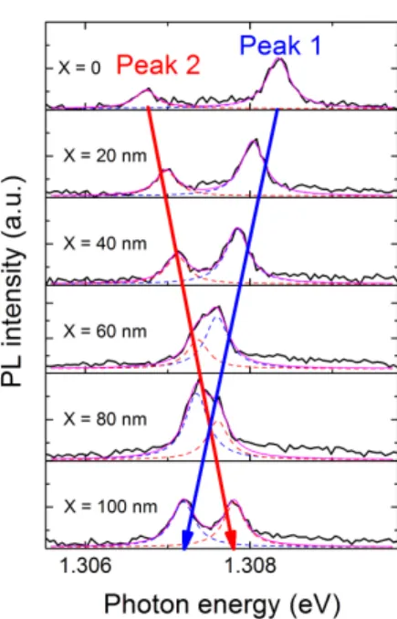
distance of 70 nm from the zero strain line (see Fig.2(c)). Since two QDs located on either sides of the zero-stress line undergo energy shifts of different signs, our technique can be exploited to easily bring two QDs in resonance. We demonstrate this possibility with a different waveg-uide sample, named S2. It features a slightly different geometry (see [16] for a complete description). As shown in Fig.3, two QDs whose emission energies initially differ by 2 meV are brought in resonance for a displacement of the top facet of 70 nm. We have also been able to use two independent nanomanipulator tips pushing along two dif-ferent arbitrary directions. This allowed us to choose and tune the direction of the applied stress gradient. The ad-ditional degree of freedom brought by a second nanoma-nipulator would make it possible to bring three QDs on resonance in the same waveguide.
Relative tuning of two QDs has already been obtained using strain gradient in different structures [25, 26]. In our work, the two QDs brought in resonance are embed-ded in a one-dimensional single mode waveguide, which opens up interesting perspective to investigate collective effects in light-matter coupling [19]. If g is the coupling
of a two level system to a single optical mode, the con-structive coherent coupling of N such two-level systems to a single optical mode gives rise to an enhanced light-matter coupling of g√N of this collective state leading
to a spontaneous emission rate accelerated by a factor N [19]. This property can be beneficial for implementing quantum memories as mentioned in the landmark paper by Duan et al [27].
We close the paper with practical considerations re-garding the observation of such collective effects. As previously mentioned, the position noise of the tip trans-lates into a spectral broadening of the QD emission lines, which is obviously detrimental for coherent effects. In our proof-of-principle experiment, the tip position noise is 1 nm. For the QD investigated in Fig.2 (70 nm away from the neutral strain line), this leads to a spectral noise of 30 µeV. State-of-the-art piezo scanners feature a po-sition noise below 0.1 nm, allowing to gain one order of magnitude on the QD linewidth. In addition, considering QDs closer to the neutral line (∼ 10 nm) leads to spec-tral fluctuations smaller than the natural QD linewidth (0.5 µeV for a 1 ns excitonic lifetime). In the same time, the tuning range remains acceptable (±4 meV for a 1 µm top facet displacement). From an optical point of view, these slightly off-axis QDs remains very well coupled to the fundamental guided mode. For a wire diameter be-low 300 nm, the spontaneous emission coupling factor is larger than 90% for QDs 10 nm away from the wire axis [28].
In summary, we have achieved a large static strain tun-ing of up to 25 meV for a semi-conductor QD embedded in an optically engineered environment using an original set-up based on photonic wires stressed by nanomanipu-lators. Thanks to the strong gradient generated within the structure, we have demonstrated differential tuning of two QDs coupled to the same single mode waveguide. This opens interesting perspectives for the demonstration of collective effects such as superradiance.
ACKNOWLEDGMENTS
Sample fabrication was carried out in the "Upstream Nanofabrication Facility" (PTA) and CEA LETI MI-NATEC/DOPT clean rooms. We thank Nitin S. Ma-lik for his contribution to the sample fabrication. D.T. was supported by a PhD scholarship from the Rhône-Alpes Region, N.V by a PhD scholarship from Fondation Nanosciences, and H.A.N. by a PhD scholarship from Vietnamese government. This work was supported by ANR project QDOT (ANR-16-CE09-0010-01) and by the CEA DRF-Impulsion project SOUPAPE.
4
Figure 3. PL spectra for different nanomanipulator positions ranging from X = 0 nm to X = 100 nm, measured on sample S2. The two peaks correspond to two QDs that are located on either side of the neutral strain line, and therefore undergo energy shifts of different signs. The two QDs are brought in resonance for X ' 70 nm.
[1] M. Munsch, N. S. Malik, E. Dupuy, A. Delga, J. Bleuse, J. M. Gérard, J. Claudon, N. Gregersen, and J. Mørk, Phys. Rev. Lett. 110, 177402 (2013).
[2] X. Ding, Y. He, Z.-C. Duan, N. Gregersen, M.-C. Chen, S. Unsleber, S. Maier, C. Schneider, M. Kamp, S. Höfling, C.-Y. Lu, and J.-W. Pan, Phys. Rev. Lett. 116, 020401 (2016).
[3] N. Somaschi, V. Giesz, L. De Santis, J.C. Loredo, M.P. Almeida, G. Hornecker, S. L. Portalupi, T. Grange, C. Antón, J. Demory, C. Gómez, I. Sagnes, N.D. Lanzillotti-Kimura, A. Lemaître, A. Auffèves, A. G. White, L. Lanco and P. Senellart, Nat. Photon. 10, 340 (2016).
[4] P. Senellart, G. Solomon, and A. White, Nat. Nanotech.
12, 1026 (2017)
[5] J.-Y. Marzin, J.-M. Gérard, A. Izraël, D. Barrier, and G. Bastard, Phys. Rev. Lett. 73, 716 (1994).
[6] P. Gold, A. Thoma, S. Maier, S. Reitzenstein, C. Schnei-der, S. Höfling, and M. Kamp, Phys. Rev. B 89, 035313 (2014).
[7] J. J. Finley, M. Sabathil, P. Vogl, G. Abstreiter, R. Oul-ton, A. I. Tartakovskii, D. J. Mowbray, M. S. Skolnick, S. L. Liew, A. G. Cullis, and M. Hopkinson, Phys. Rev. B 70, 201308 (2004).
[8] R. B. Patel, A. J. Bennett, I. Farrer, C. A. Nicoll, D. A. Ritchie and A. J. Shields, Nat. Photon. 4, 632 (2010).
[9] A. J. Bennett, R. B. Patel, J. Skiba-Szymanska, C. A. Nicoll, I. Farrer, D. A. Ritchie, and A. J. Shields, Appl. Phys. Lett. 97, 031104 (2010).
[10] S. Seidl, M. Kroner, A. Högele, K. Karrai, R. J. War-burton, A. Badolato and P. M. Petroff, Appl. Phys. Lett.
88, 203113 (2006).
[11] E. B. Flagg, A. Muller, S. V. Polyakov, A. Ling, A. Migdall, and G. S. Solomon, Phys. Rev. Lett. 104, 137401 (2010).
[12] X. Wu, X. Dou, K. Ding, P. Zhou, H. Ni, Z. Niu, D. Jiang, and B. Sun, Appl. Phys. Lett. 103, 252108 (2013). [13] P. E. Kremer, A. C. Dada, P. Kumar, Y. Ma, S.
Ku-mar, E. Clarke, and B. D. Gerardot, Phys. Rev. B 90, 201408(R) (2014).
[14] R. Trotta, J. Martín-Sánchez, I. Daruka, C. Ortix, and A. Rastelli, Phys. Rev. Lett. 114, 150502 (2015). [15] J. Martín-Sánchez, R. Trotta, A. Mariscal, R. Serna, G.
Piredda, S. Stroj, J. Edlinger, C. Schimpf, J. Aberl, T. Lettner, J. Wildmann, H. Huang, X. Yuan, D. Ziss, J. Stangl, and A. Rastelli, arXiv:1710.07374 (2017). [16] I. Yeo, P-L. de Assis, A. Gloppe, E. Dupont-Ferrier, P.
Verlot, N. S. Malik, E. Dupuy, J. Claudon, J.-M. Gérard, A. Auffèves, G. Nogues, S. Seidelin, J-Ph. Poizat, O. Ar-cizet and M. Richard, Nat. Nanotech. 9, 106 (2014). [17] M. Montinaro, G. Wüst, M. Munsch, Y. Fontana, E.
Warburton, and M. Poggio, Nano Lett. 14, 4454 (2014). [18] P.-L. de Assis, I. Yeo, A. Gloppe, H. A. Nguyen, D. Tumanov, E. Dupont-Ferrier, N. S. Malik, E. Dupuy, J. Claudon, J.-M. Gérard, A. Auffèves, O. Arcizet, M. Richard, and J.-Ph. Poizat, Phys. Rev. Lett. 118, 117401 (2017).
[19] A. Goban, C.-L. Hung, J.D. Hood, S.-P. Yu, J.A. Mu-niz, O. Painter, and H.J. Kimble, Phys. Rev. Lett. 115, 063601 (2015).
[20] H.A. Nguyen, T. Grange, B. Reznychenko, I. Yeo, P.-L. de Assis, D. Tumanov, F. Fratini, N. S. Malik, E. Dupuy, N. Gregersen, A. Auffèves, J.-M. Gérard, J. Claudon, and J.-Ph. Poizat, arXiv:1705.04056.
[21] M. Munsch, A. V. Kuhlmann, D. Cadeddu, J.-M. Gérard, J. Claudon, M. Poggio, and R. J. Warburton, Nat. Com-mun. 8, 76 (2017).
[22] H. A. Nguyen, PhD thesis, Université Grenoble Alpes (2016), https://tel.archives-ouvertes.fr/tel-01360549 [23] P.Y. Yu, and M. Cardona, Fundamentals of
semiconduc-tors, Springer ed. (2010).
[24] P. Stepanov, M. Elzo-Aizarna, J. Bleuse, N.S. Malik, Y. Curé, E. Gautier, V. Favre-Nicolin, J.-M. Gérard, and J. Claudon, Nano Lett. 16, 3215 (2016).
[25] S. Mendach, S. Kiravittaya, A. Rastelli, M. Benyoucef, R. Songmuang, and O. G. Schmidt, Phys. Rev. B 78, 035317 (2008).
[26] T. Zander, A. Herklotz, S. Kiravittaya, M. Benyoucef, F. Ding, P. Atkinson, S. Kumar, J. D. Plumhof, K. Dörr, A. Rastelli, and O. G. Schmidt, Opt. Express 17, 22452 (2009) .
[27] L.-M. Duan, M. D. Lukin, J. I. Cirac, and P. Zoller, Na-ture 414, 413 (2001).
[28] J. Bleuse, J. Claudon, M. Creasey, N. S. Malik, J.-M. Gérard, I. Maksymov, J.-P. Hugonin, and P. Lalanne, Phys. Rev. Lett. 106, 103601 (2011).