People’s Democratic Republic of Algeria
Ministry of Higher Education and Scientific Research University of Hadj Lakhdar Batna
Faculty of Technology Department of Electronics
A Dissertation Presented to the University of Batna Department of Electronics
By
Toufik BENDIB
Submitted in fulfillment of the requirement of the degree of Doctor of Science in Electronics
Entitled:
Contribution to the modeling and
improvement of the nanoscale
multigate transistors: Application to
the nanoscale circuits design
Committee members :
Dr. Abdelhamid BENHAYA Professor U. of Batna President
Dr. Fay¸cal DJEFFAL Professor U. of Batna Advisor
Dr. Zohir DIBI Professor U. of Batna Examiner
Dr. Abdelouahab BENTABET Professor U. of Bordj- Examiner Bou-Arreridj
Dr. Abdesselam HOCINI Assoc. Professor U. of M’sila Examiner Dr. Idris BOUCHAMA Assoc. Professor U. of M’sila Examiner Dr. Gian-Franco DALLA BETTA Assoc. Professor U. of Trento Invited
R´epublique Alg´erienne D´emocratique et Populaire Minist`ere de l’Enseignement Sup´erieur
et de la Recherche Scientifique Universit´e Hadj Lakhdar Batna
Facult´e de Technologie Th`ese
Pr´esent´ee au
D´epartement d’Electronique Pour l’obtention du diplˆome de Doctorat en Sciences en Electronique
Par
Toufik BENDIB
Th`eme:
Contribution `
a la mod´
elisation et
am´
elioration des transistors `
a grilles
multiple: Application `
a la conception
des circuits nanom´
etriques
Devant le jury:
Dr. Abdelhamid BENHAYA Professeur U. de Batna Pr´esident Dr. Fay¸cal DJEFFAL Professeur U. de Batna Rapporteur Dr. Zohir DIBI Professeur U. de Batna Examinateur Dr. Abdesselam HOCINI Professeur U. de M’sila Examinateur Dr. Idris BOUCHAMA M.C (A) U. de M’sila Examinateur Dr. Abdelouahab BENTABET M.C (A) U. de Bordj- Examinateur
Bou-Arreridj
Dr. Gian-Franco DALLA BETTA M.C (A) U. de Trento Invit´e (2016)
DEDICATION
Acknowledgements
First of all, I thank Allah, the Most High, the Most Compassionate, and the Most Merciful for the opportunity He gave me to study, to research and to write this dissertation. Thanks Allah, my outmost thanks, for giving me the ability, the strength, attitude and motivation through this research and to complete this work.
I would like to express my best gratitude to my advisor, Prof. DJEFFAL Fay¸cal, who accepted me as his student and has supported my whole graduate life. Without his deepest expertise and the most shrewd insight, it would not have been possible to finish this work. His in-depth knowledge, vast experiences, and his most gentle personality have set the biggest example that I wish to resemble through my career.Even more than the knowledge itself, I would like to learn and practice his clear way of thinking through my life.
I’m also grateful to my committee members, Prof. Abdelhamid BENHAYA, Prof. Zohir DIBI, Prof. Abdelouahab BENTABET Dr. Abdesselam HOCINI and Dr.Idris BOUCHAMA as well as Invited committee member Dr. Gian-Franco DALLA BETTA for taking time to serve as committee members, to review my dissertation and give valuable comments.
I appreciate my friends in university of BATNA Mr.Toufik BENTRCIA and Dr.Fouzi DOUAK for their encouragement, help and support. I would like to thank all my friends, colleagues and the staff at the Department of Electronics,University of Batna for their help along the realization of this work.
I thank to my family who have supported me with love and patience. Finally, I heartily thank to my dear fianc´e for support, and patience, which hastened my graduation. Toufik BENDIB
The work compiled in this thesis has been partially supported by the Averro`es Erasmus Mundus program funded by the European Commission (unfolding during the period of May 2013 to April 2015).
The text of Chapter 3, in part, is a reprint of the material as it appears in ”A compact charge-based model to study the nanoscale undoped double gate MOSFETs for nano-electronic circuit design using genetic algorithms” by T. Bendib, F. Djeffal, and D. Arar, Journal of Semiconductors, IOP Publishing, 2013. The dissertation author was the pri-mary investigator and author of this paper.
The text of Chapter 3, in part, is a reprint of the material as it appears in ”Fuzzy-logic-based approach to study the electrons mobility in nanoscale double gate MOSFETs” by T. Bendib, F. Djeffal, D. Arar, Z. Dibi, and A. Ferdi, IOP Conference Series: Materials Science and Engineering, IOP Publishing, 2012. The dissertation author was the primary investigator and author of this paper.
The text of Chapter 4, in part, is a reprint of the material as it appears in ”Electri-cal performance optimization of nanos”Electri-cale double-gate MOSFETs using multiobjective genetic algorithms” by T. Bendib and F. Djeffal, IEEE Transactions on Electron Devices, 2011. The dissertation author was the primary investigator and author of this paper. The text of Chapter 5, in part, is a reprint of the material as it appears in ”A two-dimensional semi-analytical analysis of the subthreshold swing behavior including free carriers and interfacial traps effects for nanoscale double-gate MOSFETs” by F. Djeffal, T. Bendib, and M. A. Abdi, Microelectronics Journal, Elsevier, 2011. The dissertation author was the primary investigator and author of this paper.
The text of Chapter 5, in part, is a reprint of the material as it appears in ”Subthreshold behavior optimization of nanoscale graded channel gate stack double gate (GCGSDG) MOSFET using multi-objective genetic algorithms” by T. Bendib, F. Djeffal, and D. Arar, Journal of computational electronics, Springer, 2011. The dissertation author was the primary investigator and author of this paper.
The text of Chapter 5, in part, is a reprint of the material as it appears in ”An opti-mized junctionless GAA MOSFET design based on multiobjective computation for high-performance ultra-low power devices” by T. Bendib, F. Djeffal, and M. Meguellati, Jour-nal of Semiconductors, IOP Publishing, 2014. The dissertation author was the primary investigator and author of this paper.
VITA
2006 Eng., Electronics Engineering, University of Batna, Batna, Algeria. 2006-2009 M.Sc., Electronics Engineering, University of Batna, Batna, Algeria.
2014 Ph.D., Electronics Engineering, University of Batna, Batna, Algeria.
PUBLICATIONS
Published Journal Papers
• T. Bendib and F. Djeffal, Electrical performance optimization of nanoscale double-gate MOSFETs using multiobjective genetic algorithms, IEEE Transactions on Elec-tron Devices, vol. 58, no. 11, pp. 37433750, 2011.
• F. Djeffal and T. Bendib, Multi-objective genetic algorithms based approach to op-timize the electrical performances of the gate stack double gate (GSDG) MOSFET, Microelectronics Journal, vol. 42, no. 5, pp. 661666, 2011.
• T. Bendib, F. Djeffal, and D. Arar, Subthreshold behavior optimization of nanoscale graded channel gate stack double gate (GCGSDG) MOSFET using multi-objective genetic algorithms, Journal of computational electronics, vol. 10, no. 1-2, pp. 210215, 2011.
• F. Djeffal, T. Bendib, and M. A. Abdi, A two-dimensional semi-analytical analysis of the subthreshold swing behavior including free carriers and interfacial traps effects for nanoscale double-gate MOSFETs, Microelectronics Journal, vol. 42, no. 12, pp. 13911395, 2011.
• T. Bendib, F. Djeffal, D. Arar, Z. Dibi, and A. Ferdi, Fuzzy-logic-based approach to study the electrons mobility in nanoscale double gate MOSFETs, in IOP Conference Series: Materials Science and Engineering, vol. 41, no. 1. IOP Publishing, 2012, pp. 012016.
• T. Bendib, F. Djeffal, and D. Arar, A compact charge-based model to study the nanoscale undoped double gate MOSFETs for nanoelectronic circuit design using genetic algorithms, Journal of Semiconductors, vol. 34, no. 4, pp. 044003, 2013.
• T. Bendib, F. Djeffal, and M. Meguellati, An optimized junctionless GAA MOSFET design based on multiobjective computation for high-performance ultra-low power devices, Journal of Semiconductors, vol. 35, no. 7, pp. 074002, 2014.
Conference Proceedings
• T. Bendib, F. Djeffal, T. Bentrcia, D. Arar, and N. Lakhdar, Multi-objective genetic algorithms based approach to optimize the small signal parameters of gate stack double gate MOSFET, in Proceedings of the World Congress on Engineering, vol. 2, 2012, pp. 46.
Book-chapter
• T. Bendib and F. Djeffal, Multi-objective-based approach to optimize the analog electrical behavior of GSDG MOSFET: Application to nanoscale circuit design, in IAENG Transactions on Engineering Technologies. Springer, 2013, pp. 315325.
i
Contents
Page Contents . . . iv List of Tables . . . v List of Figures . . . ix List of Algorithms . . . x1 Introduction and Dissertation Overview 7 1.1 Introduction to CMOS scaling . . . 8
1.2 Multi-Gate MOSFETs for Nano-Scaled ICs . . . 11
1.2.1 Multi-Gate MOSFETs: Structures and advantages . . . 12
1.2.2 Double-Gate MOSFETs: Structures and Advantages . . . 16
1.2.3 Advantages of Gate All Around MOSFETs . . . 18
1.3 Compact modeling: State of the art . . . 20
1.3.1 Overview of compact modeling of Bulk MOSFETs . . . 21
1.3.2 Overview of compact modeling of Multigate MOSFETs . . . 22
1.3.2.1 Double-Gate MOSFETs . . . 23
1.3.2.2 Gate All Around MOSFETs . . . 25
1.4 Outline of the thesis and contributions . . . 26
2 Soft Computing based methods 29 2.1 Introduction to the soft computing . . . 31
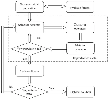
ii 2.3 Genetic algorithm . . . 33 2.3.1 Principal concept . . . 33 2.3.2 Representation . . . 35 2.3.3 Evaluating fitness . . . 35 2.3.4 Selection schemes . . . 36 2.3.5 Crossover operators . . . 38 2.3.6 Mutation operators . . . 39 2.3.7 Replacement operators . . . 40 2.3.8 Convergence criteria . . . 41
2.4 Multiobjective genetic algorithm . . . 41
2.4.1 Aggregation approach-based optimization . . . 42
2.4.1.1 Cost Function using Weighted-Sum approach . . . 43
2.4.2 Pareto front optimization . . . 45
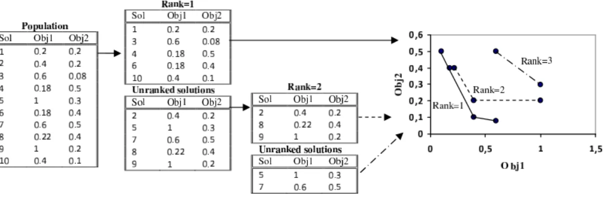
2.4.2.1 Non-dominated sorting . . . 47
2.4.2.2 Crowding distance computation . . . 48
2.5 Fuzzy logic . . . 48
2.5.1 Principal concept . . . 49
2.5.2 Fuzzy set and Membership functions . . . 50
2.5.3 Fuzzy logic rules . . . 52
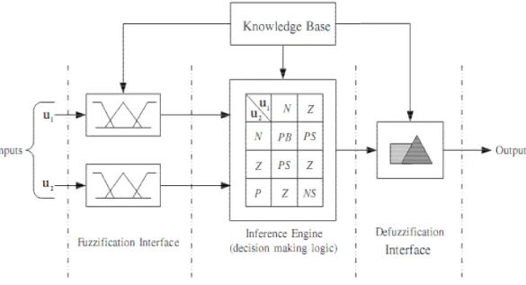
2.5.4 Fuzzy system controller . . . 53
2.5.4.1 Fuzzification interface . . . 53
2.5.4.2 Fuzzy interface inference . . . 54
2.5.4.3 Defuzzification interface . . . 54
2.6 Application of soft computing in modeling of nanoscale CMOS devices . . 55
3 Compact modeling of drain current model including quantum effects in nanoscale DG MOSFET 57 3.1 Introduction . . . 59
iii
3.3 Quantum correction using Genetic Algorithm . . . 63
3.3.1 DG MOSFET: Design description . . . 63
3.3.2 Drain current model . . . 64
3.3.3 Modeling methodology . . . 65
3.3.4 Results and discussion . . . 68
3.4 Implementation of the quantum effects in the compact drain current model 71 3.5 Electron mobility model using Fuzzy logic computation . . . 74
3.5.1 Modeling methodology . . . 75
3.5.2 Results and discussion . . . 78
3.5.3 Comparison between modeling approaches . . . 80
3.6 Sammary . . . 81
4 Design and optimization of DGMOSFETs for nanoscale circuit applica-tions 83 4.1 Introduction . . . 85
4.2 Electrical parameters of nanoscale DG MOSFET . . . 87
4.2.1 Design description of nanoscale DG MOSFET . . . 87
4.2.2 Model formulation of nanoscale DG MOSFET . . . 88
4.2.2.1 Subthreshold current . . . 88
4.2.2.2 Subthreshold swing factor . . . 89
4.2.2.3 Threshold voltage roll-off and DIBL . . . 91
4.2.2.4 Transconductance and output conductance . . . 93
4.3 MOGA-based optimization . . . 95
4.3.1 Computation methodology . . . 95
4.3.2 Results and discussion . . . 98
4.3.3 Impact on nanoscale circuits design . . . 100
4.4 Summary . . . 101 5 Modeling and optimization of subthreshold behavior for nanoscale
iv
5.1 Introduction . . . 105
5.2 Double Gate MOSFETs including free carrier and interfacial traps effect . 107 5.2.1 Description of the studied structure . . . 108
5.2.2 Model formulation . . . 109
5.2.3 Results and discussion . . . 113
5.3 Gradual Channel Gate Stack DG MOSFETs . . . 118
5.3.1 Description of the studied structure . . . 119
5.3.2 Model formulation . . . 120
5.3.3 Miltiobjective-based optimization . . . 124
5.3.4 Computation methodology . . . 125
5.3.5 Results and discussion . . . 126
5.4 Junctionless Gate All Around MOSFETs . . . 130
5.4.1 Description of the studied structure . . . 131
5.4.2 Model formulation . . . 132
5.4.3 Results and discussion . . . 135
5.4.4 Scaling capability . . . 137
5.4.5 Multiobjective-based optimization . . . 139
5.4.6 Impact on nanoscale subthreshold circuit design . . . 142
5.5 Sammary . . . 143
6 Conclusions and Future Research 145 6.1 Contributions and conclusion . . . 146
6.2 Suggestions for future work . . . 148
v
List of Tables
1.1 Scaling rules for MOSFET devices and circuit parameters . . . 10
3.1 Fuzzy associate memory table (FAM) for the fuzzy , Vthq, ξ1 and ξ2controllers. 78 3.2 Comparison between the various approaches of modeling for nano-DG MOS-FETs . . . 81
4.1 Optimized nanoscale DG MOSFET design parameters . . . 99
4.2 Optimized nanoscale single transistor amplifier design parameters . . . 101
5.1 Parameters used for MOGA-based computation . . . 126
5.2 GCGSDG MOSFET design parameters for Vgs = 0.1V and Vds = 0.5V . . 129
5.3 Optimized nanoscale JLGAA MOSFET design parameters. . . 141
vi
List of Figures
1.1 2007 ITRS product technology trends: product functions/chip and industry
average ”Moore’s Law” trends. . . 9
1.2 Scaling principle of silicon technology. . . 9
1.3 Scaling of transistor size (physical gate length) with technology node to sustain Moore’s Law”. . . 12
1.4 Ultra Thin Body (UTB) Silicon On Insolator (SOI) and Different Multi-Gate MOSFET Structures. (1:UTB SG SOI; 2:DG; 3:Tri-Multi-Gate; 4: Quadruple-Gate; 5:Ω-Gate). . . 13
1.5 Three-dimensional schematic diagram of a QG MOSFET. . . 14
1.6 Cross sectional TEM photo of a typical SG MOSFET (circular nanowire transistor). . . 15
1.7 Schematic diagram of Π-gate and Ω-gate MOSFET cross-sections. . . 15
1.8 Different topologies of DG MOSFETs: (a) Planar type; (b) Vertical type; (c) Fin type. . . 17
1.9 Development cycle for compact modeling . . . 21
1.10 Schematic diagram of a compact model for the bulk MOSFETs . . . 22
2.1 Optimization mechanism . . . 32
2.2 Flowchart for simple genetic algorithm . . . 34
2.3 Example chromosome with N parameters composed of 4 binary digits each 35 2.4 Roulette wheel selection with each slice proportional to the individual’s relative fitness . . . 37
vii
2.5 Example of single point crossover . . . 38
2.6 Example of multi-point crossover . . . 38
2.7 Example of uniform crossover . . . 39
2.8 Example of mutation operator . . . 40
2.9 Direction of search in GA with a combined fitness function . . . 45
2.10 : Illustration of non-domination and crowding for a two-objective mini-mization problem . . . 46
2.11 Illustration of non-dominated sorting procedure for a two-objective mini-mization problem from a set of randomly generated population of 10 indi-viduals . . . 47
2.12 Comparison between classical and fuzzy sets . . . 49
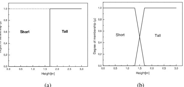
2.13 Illustration of membership functions for a set of tall people (a) crisp set (b) fuzzy set . . . 51
2.14 Triangular membership function . . . 51
2.15 Gaussian membership function . . . 51
2.16 Trapezoidal membership function . . . 52
2.17 Basic configuration of a fuzzy logic controller . . . 53
3.1 Classical (solid line) and quantum (dashed line) mobile charge sheet density Qi of symmetric DG MOSFETs in both linear (right) and logarithmic (left) scales versus gate voltage. . . 62
3.2 Schematic sketch of symmetrical DG MOSFET structure investigated in this study with (channel doping NA= 1015cm−3, tsirepresents silicon thick-ness and tox is the oxide thickness). . . 63
3.3 Flowchart of our charge-based computation approach . . . 66
3.4 (a) Classical and optimized quantum oxide capacitance versus film thick-ness (b) Classical and quantum threshold voltage versus film thickthick-ness . . . 69
3.5 Influence of the film thickness on the electron concentration distribution . . 70 3.6 Classical and corrected quantum inversion charge versus gate-source voltage 71
viii
3.7 Numerical (symbols) and calculated (solid lines) drain current vs. drain
voltage . . . 74
3.8 Flowchart of our FL-based electrons mobility computation approach . . . . 75
3.9 Electrons mobility characteristic calculated from the FL-based compact model (solid lines), compared with numerical simulations (symbols) for tsi = 5nm and tox = 1.5nm . . . 79
3.10 Evolution of the Fuzzy logic parameters versus the simulation cycle times . 80 4.1 Magnetization Schematic sketch of symmetrical DG MOSFET structure investigated in this study with (channel doping NA = 1015cm −3 , tsi repre-sents silicon thickness, L is channel length and tox is the oxide thickness) . 87 4.2 Subthreshold current as function of gate-source voltage . . . 89
4.3 Subthreshold swing versus channel length . . . 90
4.4 threshold roll-off versus channel length . . . 92
4.5 IDS− VDS characteristics for different gate voltages . . . 94
4.6 Flowchart of the proposed approach for nanoscale circuits optimization . . 97
4.7 Variations of normalized overall objective function with generations . . . . 99
4.8 Nanoscale DG MOSFET voltage amplifier . . . 100
5.1 Cross-sectional view of the DG MOSFET inner structure including the interfacial traps distribution . . . 109
5.2 Surface potential distribution for the analyzed DG MOSFET with and without interfacial traps including free carriers effects (L1 = L/2, tox = 1nm, tsi = 5nm, NA= 1016cm−3 and L = 20nm) . . . 114
5.3 Interface charges’ concentrations along the channel length for different sil-icon film thicknesses for the analyzed DG MOSFET with and without interfacial traps including free carriers effects (L1 = L/2, tox = 1nm, NA= 1016cm−3 and L = 20nm) (a) tsi = 5nm, (b) tsi = 10nm . . . 115
ix
5.4 Calculated subthreshold swing for the DG MOSFET with and without traps as a function of channel length including free carriers effects (L1 =
L/2, tox = 1nm and tsi = 5nm, NA = 1016cm −3
) . . . 116 5.5 Variation of Subthreshold swing with channel thickness for DG MOSFET
including interfacial traps and free carriers effects with (L1 = L/2, tox =
1nm, NA= 1016cm−3 and L = 30nm) . . . 117
5.6 Cross-sectional view of the GCGSDG MOSFET proposed inner structure . 119 5.7 Variation of normalized overall objective function with generations . . . 127 5.8 Variation of subthreshold swing degradation coefficient with generations . . 127 5.9 Variation of OFF-state current with generations . . . 128 5.10 Subthreshold drain current variation as function of gate and drain voltages
for different device configurations . . . 129 5.11 Cross-sectional view of the investigated JLGAA MOSFET, and the
coor-dinate system . . . 132 5.12 Subthreshold swing versus channel length with various silicon thicknesses
(tox = 3nm, ND = 1019cm−3, Vgs = 0.2V and Vds = 0.1V . . . 136
5.13 Subthreshold swing versus channel length with various oxide thicknesses (tsi = 10nm, ND = 1019cm−3, Vgs = 0.2V and Vds = 0.1V . . . 137
5.14 Design space for channel length versus silicon thickness for both JLGAA and GAA designs . . . 138 5.15 Variations of normalized overall objective function with generations . . . . 141 5.16 Nanoscale ultra-low power, JLGAA MOSFET, voltage amplifier . . . 142
x
List of Algorithms
1 Canonical genetic algorithm . . . 33 2 FL Rules . . . 77 3 Multiobjective Genetic Algorithm . . . 96
ABSTRACT OF THE DISSERTATION
Contribution to the modeling and improvement of
the nanoscale multigate transistors: Application to
the nanoscale circuits design
By
Toufik BENDIB
Doctor of Science in Electronics
University of Hadj Lakhdaru, Batna, 2014
Professor Fay¸cal DJEFFAL, Advisor
As bulk CMOS scaling is approaching the limit that is imposed by gate-tunneling leakage current, dopant fluctuation, band-to-band tunneling, etc., multi-gate MOSFET is becom-ing an intense subject of very large-scale integration (VLSI) research.Among a variety of non-classical MOSFETs, multiple-gate (MG) MOSFETs which are still based on Si have been proposed to scale down CMOS technology more aggressively because of better control of short-channel effects (SCEs).
This dissertation focuses on the design optimization and modeling of these categories of multiple-gate (MG) MOSFETs to improve device performances for nanoscale circuits de-sign applications.
In this dissertation, we will first introduce the complete analytic models of drain current by assuming gradual channel approximation(GCA) to derive the Current-Voltage(I-V) char-acteristic of short channel Double Gate (DG) MOSFET with intrinsic silicon body using the effective electric field-charge density relationship. Thus, the mobility degradation effect
which mainly depend on the inversion charge distribution in the channel is incorporated in the model at high electric field. Moreover, the developed models should be able, includ-ing quantum effect (QE), to correctly represent the I-V characteristics of the nanoscale DG MOSFET, and effectively capture the electrical behavior of the device due to process variations. The proposed I-V model is continuously valid from the subthreshold to the quasi-linear regime operation and up to a well-defined drain saturation voltage and agrees with 2D Silvaco and nanoMOS2.5 numerical simulations. In addition, the proposed mod-els have several advantages such as accuracy, simplicity and applicability for device with a wide range of dimension.
This work used a new soft computing approach, multiobjective genetic algorithm(MOGA), which allows investigation and simulation of the nanoscale (multigate) CMOS-based de-vices. The effects of device design parameters like silicon channel thickness, gate oxide thickness, and silicon channel length are studied and the output electrical parameters of the device such as OFF-sate current and subthreshold swing factor, threshold voltage rool-off, DIBL and small signal parameters are analyzed for a wide range of electrical and geometrical parameters. The key idea of the proposed approach is to optimize the elec-trical behavior of the DG MOSFET for subthreshold and saturation regime by satisfying of the following objective functions: Minimization of the OFF-current state:IOFF, Mini-mization of the subthreshold swing degradation coefficient, MiniMini-mization of the threshold voltage roll-off, Maximization of the transconductance function and Minimization of the output conductance function. The obtained results provide to the circuit designers several optimal solutions to choose the one that suites best his analog and/or digital application. The adopted designs can be exported to meet the targets for analog and digital applications simultaneously.
This work also develops subthreshold models for nanoscale multiple-gate MOSFET based on surface potential formalism. The analytical solutions of electrostatic potential and sub-threshold current are validated by their agreement with 2D numerical simulation. These models allow the subthreshold swing, OFF-state current and scaling length to be formulated as objective functions, which are the pre-requisite of MOGA application.
This approach is applied to find optimal subthreshold parameters where superior electri-cal performances in subthreshold regime are provided by the proposed devices and offers ultra-low power consuming and high-speed commutation required for analog and digital application respectively. Moreover, in this work we deal with a new structure of MG transistors, which is the JLGAA MOSFET. This latter is considered as straightforward designs to eliminate some technological limitations for nanoscale applications, such as ultra-abrupt junctions, low cost fabrication.
Keywords: Nanoscale, Multigate, Quantum, Short channel, Analog, Digital, Optimiza-tion, Modeling, Soft computing, Genetic algorithm.
R´
esum´
e
Comme la r´eduction des dispositif CMOS approche la limite qui est impos´e par le courant de fuite de grille dˆu `a l’effet de tunnel, la variation du dopant et l’effet tunnel bande `a bande, etc..., MOSFET `a grilles multiple devient un axe tr`es intense de recherche de l’int´egration `a grande ´echelle (VLSI). Parmi une vari´et´e de MOSFET non-classiques, MOSFET `a grilles multiple (MG) `a base de Si ont ´et´e propos´ees pour r´eduire agressive-ment la technologie CMOS grˆace `a un meilleur contrˆol des effets de canaux courts (SCEs). Cette th`ese est consacr´e `a l’optimisation et la mod´elisation de ces cat´egories MOSFETs `a grilles multiple pour am´eliorer les performances des dispositifs pour la conception des circuits `a l’´echelle nanom´etrique.
Dans cette th`ese, en premier lieu, on va introduire le mod`ele analytique du courant de drain en tenant en compte l’approximation du canal gradu´e (GCA) pour obtenir la car-act´eristique courant-tension (I-V) du transistor Double Gate (DG) MOSFET `a canal court pour le cas d’un substrat de silicium intrins`eque. Ce mod`ele utilise la relation entre le champ ´electrique et la densit´e de charge et inclut l’effet de la d´egradation de la mobilit´e, qui d´epends de la distribution de la charge d’inversion, dans le mod`ele pour les champs ´electriques ´elev´es. En outre, le mod`ele d´evelopp´e devrait ˆetres capable de repr´esenter la caract´eristique I-V correctement du transistor DG MOSFET `a canal court en tenant compte les effets quantiques(QE), et de capturer avec ´efficacit´e le comportement ´electrique du dispositif en prenant en compte les effets du processus de conception. Le mod`ele I-V propos´e est en accord avec les simulations num´eriques (2D Silvaco et nanoMOS2.5) et valide pour tous les r´egimes de fonctionnement (sous le seuil, le r´egime quasi-lin´eaire et le r´egime de saturation). En plus, les mod`eles d´evelopp´es sont simples, pr´ecis, est ad´equats pour de larges gammes de g´eom´etrie.
Ce travail a utilis´e une nouvelle m´ethode de calcul intelligent (SC), algorithme g´en´etique multi-objectifs (MOGA), qui permet l’´etude et la simulation des dispositifs MG `a l’´echelle nanom´etrique. L’ effets des param`etres de conception du dispositif, comme l’´epaisseur du
canal de silicium, l’´epaisseur d’oxyde de grille et la longueur du canal de silicium sont ´etudi´ees o`u les param`etres ´electriques qui repr´esentent la sortie du dispositif, tels que le courant de fuite OFF-current, l’inverse de la pente sous seuil, la tension de seuil rool-off, DIBL et les param`etres petits signaux sont analys´es pour une large gamme de param`etres ´electriques et g´eom´etriques.
L’id´ee cl´e de l’approche propos´ee est d’optimiser le comportement ´electrique du transis-tor DG MOSFET dans le r´egime sous-seuil et le r´egime de saturation simultan´ement en satisfaisant les fonctions objectifs suivantes: minimisation de OFF-current, minimisation de la d´egradation de l’inverse de la pente sous seuil, minimisation de la tension de seuil roll-off, maximisation de la fonction ”transconductance” et la minimisation de la fonction ”output-conductance”.
Ce travail d´eveloppe aussi des mod`eles sous-seuils des MG MOSFET `a l’´echelle nanom´etrique en se basant sur l’analyse du potentiel de surface ´electrostatique. Les solutions analytiques du potentiel ´electrostatique et du courant sous seuil sont valid´ees par leur accord avec la simulation num´erique 2D. Ces mod`eles permettent : l’inverse de la pente sous seuil, OFF-current et le param`etre de la r´eduction du canal pour ˆetre formul´es comme des fonctions objectifs, qui repr´esentent le pr´e-requis du MOGA.
Cette approche est appliqu´ee afin de trouver les param`etres sous-seuils optimaux qui four-nissent des performances ´electriques sup´erieures dans le r´egime sous-seuil et offrent une faible consommation de puissance et une haute vitesse de commutation qui sont n´ecessaires pour les applications analogiques et num´eriques respectivement. En plus, dans ce travail, on traite une nouvelle structure de transistors `a grilles multiples: le transistor `a grille enrob´ee sans jonction JLGAA MOSFET, qui est consid´er´e comme une simple conception des transistors MOSFETs. Ce dernier permet d’´eliminer certaines limitations impos´ees par la technologie nanom´etrique, telles que les jonctions ultra-brutales et le cout de fabri-cation.
Mots-cl´es: ´Echelle nanom´etrique, Grilles Multiples, Quantique, Canal court, Analogique, Num´erique, Optimisation, Mod´elisation, calucul intelligent, Algorithme g´en´etique.
Chapter 1
Introduction and Dissertation
Overview
Contents
1.1 Introduction to CMOS scaling . . . 8 1.2 Multi-Gate MOSFETs for Nano-Scaled ICs . . . 11 1.2.1 Multi-Gate MOSFETs: Structures and advantages . . . 12 1.2.2 Double-Gate MOSFETs: Structures and Advantages . . . 16 1.2.3 Advantages of Gate All Around MOSFETs . . . 18 1.3 Compact modeling: State of the art . . . 20 1.3.1 Overview of compact modeling of Bulk MOSFETs . . . 21 1.3.2 Overview of compact modeling of Multigate MOSFETs . . . . 22 1.3.2.1 Double-Gate MOSFETs . . . 23 1.3.2.2 Gate All Around MOSFETs . . . 25 1.4 Outline of the thesis and contributions . . . 26
Chapter 1. Introduction and Dissertation Overview
1.1
Introduction to CMOS scaling
Although the original idea of field effect transistor (FET) was patented as early as 1930 by Lilenfeld [1]. The first metal-oxide-semiconductor field-effect transistor (MOS-FET) on silicon substrate using SiO2 as the gate insulator was fabricated by Khang and
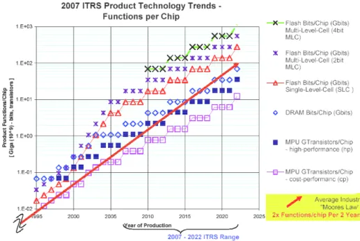
Atalla in 1960 [2]. After 3 years ago, the CMOS (complementary MOS) is invented by Wanlass and Sah [3], then integrated-circuits (ICs) have gone from having few transistors to hundreds of millions of transistors [4]. The scale down of CMOS device dimension in conventional bulk silicon CMOS technology has been a primary driver over the past three decades in order to attain continued improvement in ICs performance, reduction in size, higher compactness, lower cost, higher circuit speed, lower power dissipation, and better functionality. CMOS is considered as the crucial material base in the evolutionary progress leading to the powerful and versatile electronic systems such as computers and communication devices. The industry’s ability to exponentially reduce the minimum fea-ture sizes used to fabricate the integrated circuits ICS, has resulted exponential growth in the number of transistors and memory bits per chip popularly known as Moore’s law [5], which describes the evolution of transistor density in integrated circuits [6–11]. It affirms that the number of transistors per chip will quadruple every three years or double every 18 months [12] as shown in Figure 1.1.
Figure 1.2 illustrates the scaling concept of silicon technology, in which the device dimensions and device voltages are scaled down and the doping concentration is scaled up by the same factor [13]. Then, according to basic electrostatics, the electric field con-figuration will be the same as the original device. A larger FET can then be scaled down to a smaller FET with similar behavior.
Chapter 1. Introduction and Dissertation Overview
Figure 1.1: 2007 ITRS product technology trends: product functions/chip and industry average ”Moore’s Law” trends.
Figure 1.2: Scaling principle of silicon technology.
Table 1.1 shows the scaling rules for MOSFET devices and circuit parameters. It is shown that these scaling rules only give us a guideline to shrink down a device. They do not tell us how small we can make the devices [13]. For a given supply voltage and a given layer thickness, as the channel length decreases, the MOSFET current increases, and the intrinsic capacitance decreases. Therefore, the MOSFET switching speed is improved. However, the device channel length cannot be arbitrarily reduced because of short channel effects (SCEs) such as threshold voltage rolloff, subthreshold slope degradation and strong
Chapter 1. Introduction and Dissertation Overview
drain induced barrier lowering (DIBL) effect.
Besides the scaling limit of channel length imposed by SCEs, there are other scaling limits imposed by the reduction of the vertical thickness of MOSFETs, the gate oxide thickness, which offers better control of the gate over the channel, improves the short-channel behavior and enhances the driving capability of MOSFETs. However, ultrathin gate oxide will lead to high gate leakage current due to direct tunneling. Details of those limits have been summarized in [14]. There are various approaches to avoid those scaling limits: continue scaling down the MOSFET without changing the oxide thickness; change the device structure such that the devices can be scaled further down while the short channel effect is still under control; change the gate insulator material with higher permittivity (high-K) instead of SiO2 to increase the physical thickness while maintaining
the same effective-oxide-thickness [14, 15]. In addition, the increase of random dopant fluctuation with shrinking device size affect the threshold voltage variation from device to device. These effects lead to unacceptable high leakage current and constitute the limiting factors of CMOS scaling at present [16].
Table 1.1: Scaling rules for MOSFET devices and circuit parameters
Physical parameter Constant electric Generalized Generalized selective field scaling factor scaling factor scaling factor Channel length, Insulator thickness 1/α 1/α 1/αd
Wiring width, channel width 1/α 1/α 1/αw
Electric field in device 1 ε ε
Voltage 1/α ε/α ε/αd
On-current per device 1/α ε/α ε/αw
Doping α εα εαd Area 1/α2 1/α2 1/α2 w capacitance 1/α 1/α 1/αw Gate delay 1/α 1/α 1/αd Power dissipation 1/α2 ε2 /α2 ε2 /αdαw Power density 1 ε2 ε2 αw/αd
Chapter 1. Introduction and Dissertation Overview
In table 1.1, α represents the dimensional parameter, ε is the electric field scaling prameter, αd and αw are separate dimensional scaling parameters for the selective scaling
case. αd is applied to the device vertical dimensions and gate length, αw applies to the
device width and the wiring.
To solve these scaling issues, two different paths can be followed. The introduction of new technologies and new materials into the conventional planar bulk MOSFET can be used as first path to allow further scaling and improve the performance of scaled transistors. Moreover, the adoption of new transistor architectures such as ultra-thin body FETs and multi-gate FETs to allow superior electrostatic control over the inversion channel. In order to study the circuit level benefits and reliability of these two CMOS scaling solutions, suitable understanding and modeling of the associated device physics and device behavior is needed.
1.2
Multi-Gate MOSFETs for Nano-Scaled ICs
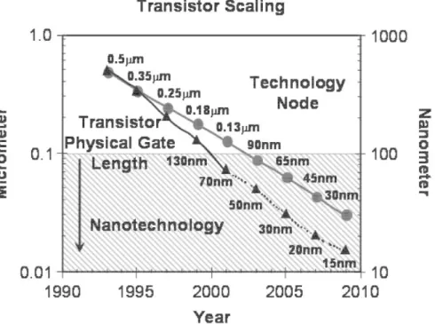
As mentioned in section 1.1, CMOS has been scaled into the deep sub-100 nm regime [17,18], and is thought to be the dominant technology in the near future. As presented in Figure 1.3 , the physical gate length is estimated to be at least at or below 10 nm according to the 22-nm technology node [19]. However, CMOS scaling seems to be fundamentally limited due to several non-ideal effects which must be taken into account in nanoscale devices [14, 20, 21]. They are mainly well-known as,
• Short-channel effects including threshold voltage roll-off, drain-induced barrier low-ering (DIBL), and subthreshold slope degradation
• Quantum mechanical effects leading to significant gate-tunneling leakage current, threshold voltage shift and gate capacitance degradation
• Random dopant fluctuation resulting threshold voltage variation • Non-negligible parasitic components.
Chapter 1. Introduction and Dissertation Overview
These effects lead to unacceptably high Off-current and degraded switching speed(swing factor and DIBL), therefore become limiting factors of further CMOS scaling at present [16].
Figure 1.3: Scaling of transistor size (physical gate length) with technology node to sustain Moore’s Law”.
1.2.1
Multi-Gate MOSFETs: Structures and advantages
As a solution to overcome these undesirable effects, new FET architecture the Multi-gate (MG) FET has been proposed and investiMulti-gated [22], including double-Multi-gate (DG), quadruple-gate, surrounding-gate (SG) [23], tri-gate [24], Pi-gate [25], Omega-gate [26] MOSFETs and FinFETs [27]. Different Multi-Gate MOSFET structures are shown in Figure 1.4, adopted from [25].
Besides the advantages of electrostatic integrity, MG MOSFETs also have some other potential promises. In MG MOSFETs, the SCEs are more controlled by the dimensions of silicon and oxide films in which the subthreshold slope (SS) degradation is not very noticeable where it is well known that the ideal SS by ignoring short-channel degradation is 60mV/Decade [28].
Chapter 1. Introduction and Dissertation Overview
Figure 1.4: Ultra Thin Body (UTB) Silicon On Insolator (SOI) and Different Multi-Gate MOSFET Structures. (1:UTB SG SOI; 2:DG; 3:Tri-Gate; 4: Quadruple-Gate; 5:Ω-Gate).
In MG MOSFETs, as the silicon film is usually undoped or lightly doped, the mobil-ity is better than bulk or Partially Depleted (PD)SOI MOSFETs because of the absence of strong impurity scattering, thus the threshold voltage variation caused by the dopant fluctuation will also be suppressed in MG MOSFETs. Moreover, MG-FETs can be con-sidred as an extension to the ultra-thin (UT) body FETs or the fully-depleted (FD) SOI FETs but with more gates around the thin silicon body, where MG-FETs offer stronger electrostatic control of the inversion channel through the use of multiple gates. The chan-nel length can be reduced to 5 times the film thickness without causing serious SCEs. Therefore, UTB-SOI with intrinsic channel and MG structures are regarded as the most promising by most research groups [23, 29, 30].
For instance, The gate controllability of the DG MOSFET is improved by both gates since the silicon film is fully depleted. In addition, The electric field lines from the source to the drain is blocked by the bottom gate electrode and therefore cannot reach the chan-nel, thus the channel length can then be reduced to 2 ∼ 3 times the film thickness in the DG configuration.
Although, it is easy to be scaled down the DG MOSFET, but it is more difficult to fabricate a gate under single crystal channel. As an example, Selective Epitaxial with Lateral Over-growth (SELO) is a pattern for planar DG fabrication [31]. Another example is the Gate-All-Around (GAA) MOSFET fabricated in [32] and [33].
Chapter 1. Introduction and Dissertation Overview
Figure 1.5: Three-dimensional schematic diagram of a QG MOSFET.
GAA MOSFET can provide the best controllability of SCEs which is usually fabricated using a Si nanowire structure, which is sometimes called nanowire transistor. Nanowire transistors have generated much research interest lately [34, 35], highlighting two types of geometry: one has rectangular (or square) shape, and is usually named quadruple-gate (QG) MOSFET; the other has circular shape, and is always called surrounding-gate (SG) MOSFET or Gate-All-Around (GAA). A 3-D schematic diagram of a QG MOSFET is illustrated in Figure 1.5 adopted from [36], whereas a typical cross sectional TEM photo for SG MOSFET is shown in Figure 1.6, adopted from [37].
Vertical DG MOSFET (Fin-FET) has also been fabricated by many research groups [38, 39]. The Fin-FET process easily provides two self-aligned gates, but this process requires a thinner fin with a width smaller than half of the gate length. Since the gate length is normally the smallest dimension in conventional MOSFET technology, the Fin-FET process has to acquire more expensive lithography equipments, thus it needs some special technologies to fabricate the silicon fin stably without lithography.
Tri-gate MOSFETs were proposed to solve this drawback [40]. Tri-gate MOSFETs use three gates coupling instead two gates coupling as in the DG MOSFET, hence they could overcome the tough fin width requirement. In addition, Tri-gate MOSFETs have
Chapter 1. Introduction and Dissertation Overview
Figure 1.6: Cross sectional TEM photo of a typical SG MOSFET (circular nanowire transistor).
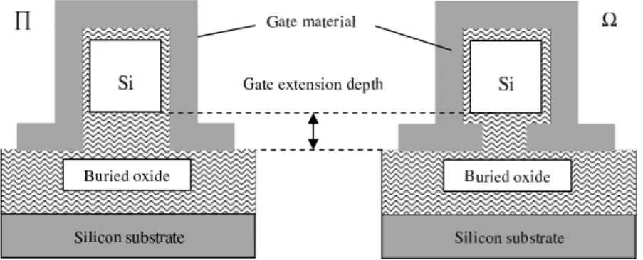
better characteristics than DG MOSFETs in terms of control of SCEs where the Fin width can be adjusted to be equal to the gate length in 30nm Tri-Gate MOSFET without causing serious SCEs [24]. However, Tri-gate MOSFETs suffer more from quantum-mechanical effects due to 2-D quantum confinement. Π-gate and Ω-gate MOSFETs are simple variations of TG MOSFETs. They can be classified into triple-plus-gate (TPG) MOSFETs because these devices are basically TG devices with an extension of the gate electrode below the active Si island, which increases current drive and can effectively improve the SCEs since the bottom channel is the bottleneck. The schematic diagram for Π-gate and Ω-gate MOSFET cross-sections is shown in Figure 1.7, adopted from [41].
Figure 1.7: Schematic diagram of Π-gate and Ω-gate MOSFET cross-sections. 15
Chapter 1. Introduction and Dissertation Overview
As discussed above, there is a clear lack of consensus as to which device approach would be the better design approach and therefore a potential candidate for replacing the conventional planar MOSFET. Each of the four multi-gate devices appears to offer some improvement in performance to the planar MOSFET. Each device however also remains to be optimized. The FinFET, for example, could be possibly tuned to outperform the TriGate device. In that case, the ease in fabrication offered by the TriGate transistor could then be offset by the performance advantage offered by the FinFET. On the other hand, given a certain fabrication technology and associated design rules, the TriGate transistor approach could result as the only viable alternative, possibly making the FinFET option impractical.
If the Ω-gate’s fabrication is further perfected, it could offer a superior performance to the FinFET and TriGate MOSFETs. These arguments although speculative, hint at the uncertainties pending in the MG SOI device arena. What would be useful is a clear and systematic experimental study to investigate the behavior of the MG devices in greater detail and understand their performance limitations in the light of design tol-erances. Considering the difficulty and the costs involved in undergoing such a thorough experimental investigation, a common simulation study comparing these devices would be desirable. Due to the dimensional nature of these devices in comparison with the conven-tional MOSFET, two and three-dimensional fabrication process and device simulations are needed to perform this comparison.
1.2.2
Double-Gate MOSFETs: Structures and Advantages
The most intensively studied MG MOSFETs are DG MOSFETs [42,43]. The possible orientations of DG MOSFET on a silicon wafer are shown in Figures 1.8(a), 1.8(b), 1.8(c), adopted from [44]. The planar DG (Figure 1.8(a)) resembles the planar bulk MOSFET technology. It has less geometry effects such as ”Corner effects” [45] and ”Narrow width effects” [46]. In addition, the planar DG is free from ”crystal plain orientation uncer-tainty” problems when directions of the devices vary. Another advantage of planar DG
Chapter 1. Introduction and Dissertation Overview
MOSFET, is that the two gates are easy to be separately biased as the two gates are formed in different process steps. In fact, these above mentioned advantages are a great reason to study DG physical properties and improve their electrical performances for such application.
Figure 1.8: Different topologies of DG MOSFETs: (a) Planar type; (b) Vertical type; (c) Fin type.
The vertical DG (Figure 1.8(b)), has the channel in the vertical direction, it is most compact for DRAM application [47] with low leakage current, however it is topologically difficult for a CMOS logic application [44]. Moreover, it is very difficult to fabricate the vertical DG, especially due to the control of the vertical doping profile, and showing no potential advantages comparing to the FinFET.
Currently, the Fin type (Figure 1.8(c)) seems to be the most promising structure, 17
Chapter 1. Introduction and Dissertation Overview
which is being studied by many groups [38, 39, 48, 49]. In FinFET DG MOSFET, the current flows horizontally through the fin channel, has the highest packing density for high speed logic applications, since the channel width, the longest dimension of a logic FET, is perpendicular to the plane of the wafer [44].
Among those above device, one of the most important device structures is planar DG MOSFET, which is selected for studying their electrical performances where the interest of this thesis is in device design and basic physical modeling. One of the greatest reason to deal with this kind of MG MOSFETs is the scaling capability to the shortest channel length for a given gate oxide thickness, (because the bottom gate can effectively screen the field penetration from the drain), hence suppress the short channel effects. We can cite these advantages as: (a)ideal 60mV/decade subthreshold slope [50]; (b)scaling by silicon film thickness without high doping; (c)setting of threshold voltage by gate work functions [51], (d) easy fabrication because of its planner structure, etc...
In this thesis, the focus will be put on the compact modeling for of planar DG MOS-FET. Our group has worked on analytic surface potential and threshold voltage models for DG MOSFETs several years before [52]. One of the contributions of this thesis is to extend the DG model according to the charge concentration evaluation including short channel and quantum effects. Then, the developed accurate analytical models, for sub-threshold and saturation regimes, will be used to improve the electrical performances of the DG MOSFETs for nanoscale applications. Efforts will also be focused on making the physics-based model more versatile and computationally efficient using soft computing approaches.
1.2.3
Advantages of Gate All Around MOSFETs
As discussed above, the UTB SOI MOSFETs can be fabricated in different forms it may be a single or double gate, a cylindrical gate or quadruple gate MOSFET. GAA MOSFET devices presented in section 1.2.1 with undoped channel has been applied for different applications. It is suitable for digital applications and have found places
Chapter 1. Introduction and Dissertation Overview
in varieties of applications like base-band analog applications, memory applications etc. The GAA MOSFETs are considered to be among the most prominent multigate CMOS devices for future generation Nano-scale IC technology due to their important advantages cited as:
• Better scalability than the double-gate MOSFETs (i.e., better control of SCE).The reason behind that the surrounding gate creates an electrical sheltering action for lateral electrical fields creating due to the charges in the source and drain. The superior scalability of the device could make the GAA MOSFET suitable for future generation CMOS technology with gate-length scaled below 25nm.
• Better switching characteristics where an ideal Subthreshold swing of 60mV/Decade could be expected in a GAA gate MOSFET. This may provide higher ON-to-OFF current ratio than that of the bulk MOSFET thereby providing better switching characteristics.
• Higher drive current since the current flow across all surrounding surface of the silicon body (not only just from the top edge as well as bottom edge in the ultra-thin body SOI DG MOSFET), the ON-state drive current can practically be greater of that of the double-gate device.
• Higher transconductance and greater linearity of GAA MOSFETs can be achieved by increasing the doping level in the channel region of device. It may be mentioned that the doped GAA MOSFETs are important for many analog and RF applications. In fact, our research group has focused on the analytical analysis of GAA MOSFETs including hot-carrier effects in order to study the scaling limits of GAA MOSFET several years ago [53]. In this thesis, our research is focused on investigation of new kind of GAA MOSFET called Junctionless (JL) GAA MOSFET which exhibits better performance with respect to GAA mosfet in term of fabrication process. Effort will also be focused on development of new subthreshold swing and scaling length models in order to illustrate the
Chapter 1. Introduction and Dissertation Overview
scaling capability of the JLGAA for ultra-low power nanoscale CMOS-based applications over GAA MOSFET design.
1.3
Compact modeling: State of the art
A compact model provides a link between process technology and circuit design. It mathematical describes the complex device physics in a transistor where it retains the fine balance between accuracy and simplicity. An accurate model based on physic allows the process engineer and circuit designer to make projection beyond the available silicon data (scalability) for scaled dimensions and also enable fast circuit and device co-optimization. The simplifications in the physics allow mathematical approximations and by consequence enable very fast analysis of device/circuit behavior in comparison with the much slower numerical simulators. Thus, it is necessary to develop a compact model for MG MOSFETs for technology circuit development in the short term and for product design in the longer term.
One of the biggest challenge is modeling MG FETs is the need to model several flavors of MG FETs. The silicon body can be controlled by either two gates, three gates or four gates. The gates can all be electrically interconnected or they can be independently biased. Multigate FETs can be built on SOI or bulk silicon. It is important to obtain a flexible model which can model all the type of Multigate FETs without making the model computationally intense. Figure 1.9 shows the development cycle of the compact model
Chapter 1. Introduction and Dissertation Overview
Figure 1.9: Development cycle for compact modeling
1.3.1
Overview of compact modeling of Bulk MOSFETs
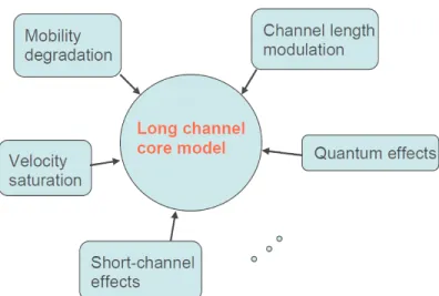
As mentioned in section 1.1, MOSFET has been the main component of integrated circuits ever since its invention. Therefore, compact modeling of MOSFETs has also been continuously growing for complex circuit design. Compact model of MOSFETs usually based on a precise core model (long channel classical model) then all specific physical phenomena that include quantum effects, short channel effects, channel length modulation,etc..., are implemented into this core model as parameter corrections in order to achieve fast and accurate circuit simulation results.
Figure 1.10 shows the schematic diagram of a compact model for a MOSFET. The evolution of MOSFET compact model starts from simple, piecewise, to complicated mod-els, continuous models to achieve more accurate circuit simulations. For example the earliest versions of BSIM model, (piecewise models), which perform separate equations
Chapter 1. Introduction and Dissertation Overview
Figure 1.10: Schematic diagram of a compact model for the bulk MOSFETs
based on the charge sheet approximation for different operation regions. This leads to the discontinuous first order derivates of current and charge and hence rigorous convergence. Non-physical mathematical smoothing functions are adopted in recent BSIM3/BSIM4 models in order to manually connect the different operation regions, as well as to over-come the convergence problem [54]. Although this approach largely solves the convergence problem, the non-physical smoothing equations fail to physically describe the transition region where MOSFET transistors in analog circuits are commonly biased.
To avoid the disadvantages of BSIM models, the surface potential models developed by the Pennsylvania State University and Philips (PSP) [55] and those developed by the Hiroshima University Semiconductor Technology Academic Research Center (HiSIM) [56] have been presented as the next generation of compact model for bulk MOSFETs. Without introducing the threshold voltage, one single surface potential equation valid for all the operation regions is solved for the solution in these models.
1.3.2
Overview of compact modeling of Multigate MOSFETs
The MG devices that control the channel from multiple sides and very thin body devices are new to circuit and system designers. These devices need to be modeled to understand and predict the functionality of the circuits. Compact device models are used
Chapter 1. Introduction and Dissertation Overview
in circuit design. New compact models that accurately model these novel devices, and are computationally efficient, are in development. There are new physical effects that now need to be incorporated into these device models.
The use of multiple gate devices in circuit design is critically dependent on the avail-ability of accurate models for these devices, valid for DC, AC, transient and noise analysis. Using appropriate models, circuit simulation allows to design circuits with devices of ad-equate dimensions. Circuit simulation requires accurate models of the current and the terminal charges (from which capacitances are obtained) of the devices. These models should be based on expressions with a sufficiently high order of continuity. Lack of con-tinuity between the different operating regimes leads to convergence problems in circuit simulation. In conventional MOSFETs, there have been a trend to move from piecewise models (with continuity problems) to unified models with an infinite order of continuity. Smoothening functions are often used to assure the continuity between different oper-ating regimes. For the same reasons, multiple-gate MOSFETs will need unified highly continuous models.
For proper modeling of nanoscale MOSFET for VLSI circuit simulation, accurate and physics-based compact models are required. The modeling principles for these devices are somewhat different from conventional bulk MOSFETs, since volume conduction should be considered.
1.3.2.1 Double-Gate MOSFETs
As discussed in the last section, the compact model development for bulk MOSFETs has shown that an ideal long channel core model should be continuous, symmetric, physics-based, accurate and computationally efficient are still a modeling challenge. These require-ments set the objective of the compact modeling of DG MOSFETs. Previous work mostly focused on the modeling of some particular physical phenomenon have been made to im-plement compact models giving insight to understand the physics and operation of DG MOSFETs. For instance, a core model for DG MOSFETs was developed by Taur based on the solution of 1-D Poisson and current continuity equations where the charge-sheet
Chapter 1. Introduction and Dissertation Overview
approximation is not taken into account [28, 57].
A number of attempts have been made to approximate these expressions including intermediate parameters in order to express the body potential, inversion charge, and drain current [58, 59]. In these works, the electric characteristics of DG MOSFETs is described as functions of charges, where obtained charge equations are still implicit, thus there is no mathematical advantage to remove the intermediate parameters. In addition, each approximation initiate nnegligible error either in the transition region or on-current regions.
Numerical study of the body doping effects on double-gate MOSFET characteristics is suggested in [60]. After that the threshold voltage shift and the subthreshold current slope degradation are discussed intensively following by an analytical solution to the 1-D Poisson’s equation [61]. Because it is impossible to solve three coupling implicit equations analytically, a series of appropriate assumptions were involved to solve the equation in a non-coupling way.
The short-channel effects were taken into account by solving 2-D Poisson’s equation in evanescent mode which is largely adopted by the bulk MOSFETs [62, 63], or assum-ing parabolic potential shape [64, 65]. Whereas, the obtained solution accordassum-ing to the parabolic potential assumption is less accurate at the silicon-silicon dioxide interface. Ex-plicit expressions for threshold voltage roll-off [66–68] and subthreshold [69] current slope were also developed [63] by solving the current continuity equation basing on the minimum potential barrier along the channel.
Furthermore, when quantum effects dominate, there still lacks a comprehensive com-pact model for DG MOSFETs. Several approaches have been applied to study quantum effects in DG MOSFETs, such as the nonequilibrium Greens function [70], density gra-dient model [71, 72], and Monte Carlo simulation [73–75]. However, these mathematical complex models make them impractical for compact modeling.
In another work, only the potential and charge distribution have been carried out by the analysis of quantum subband energy levels [76] and the quantum threshold shift [77], but no drain current equation has been developed for a compact model.
Chapter 1. Introduction and Dissertation Overview
Recently, an implementation of an analytic potential-based terminal charge and capac-itance model was carried out for AC and transient simulations [78]. Employing different forms of drain current expression results in similar expressions for the terminal charges and capacitances [79].
In this context, we apply in chapter 3 a soft computing approaches particulary Genetic Algorithm, Fuzzy Logic to implement quantum effects into an analytic charge model as quantum corrections for DG MOSFETs in order to develop continuous quantum drain current model close to NEGF numerical simulation.
1.3.2.2 Gate All Around MOSFETs
Most of the existing GAA MOSFET models are based on one-dimensional (1-D) analy-sis, and are suitable only for long channel devices [80]. As consequence, they are unable to reproduce the roll-off as the channel length is reduced. A two-dimensional analysis is nec-essary to derive threshold voltage and subthreshold swing models that properly account for the channel length dependence. A few 2-D models of the threshold voltage for doped and undoped GAA MOSFETs have been presented [81, 82]; however, all of them neglect the effect of the mobile charge density, which can be important in the near-threshold regime (in particular for undoped devices).
Furthermore, simple continuous analytic current-voltage (I-V) model for cylindrical undoped (lightly doped) GAA MOSFETs where the charge-sheet approximation allowing adequately capture of inversion charge distribution in the silicon [83].
Recently, Hamedy et.al., have proposed an analytical, physically-based, models for the threshold voltage, the subthreshold swing and DIBL of undoped cylindrical Gate All Around (GAA) MOSFETs which have been derived based on an analytical solution of the two-dimensional (2-D) Poisson equation (in cylindrical coordinates) including the mobile charge term, by using new techniques that allow to consider the effect of channel length, thickness and drain-source voltage [84]. His model is validated by comparison with the results obtained from 3-D numerical simulations with DESSIS-ISE for different channel lengths/thickness and from low to high drain-source voltage values.
Chapter 1. Introduction and Dissertation Overview
As an extended work, Hamdy et.al have developed an analytical and continuous DC models for cylindrical undoped GAA MOSFETs, in which the channel current is written as an explicit function of the applied voltages [80]. The model is based on a new unified charge control model developed for the device. The explicit model shows good agreement with the numerical exact solution obtained from the new charge control model, which was validated by comparison with 3D numerical simulations.
Another compact models for GAA MOSFETs [85] have been recently developed us-ing several approximation in order to derive analytical solutions of Poisson’s equation for doped and undoped devices. In this work, self-consistency with Schr¨odinger’s equation combined with the current continuity equation are addressed to describe the carrier trans-port models. Thus, it overcome some difficulties in compact modeling :the electrostatics, the quantum effects, the transport mechanisms, and the high-frequency behavior.
1.4
Outline of the thesis and contributions
The main goal of this work is to apply new soft computing approaches in order to improve the computational performance in term of computing time and accuracy, pro-pose new design structures of nanoscale multigate MOSFETs to study their electrical performances for digital and analog applications. Moreover, both analytical and compact models are developed to be exported to the IC design community worldwide. This disser-tation is devoted to the design, modeling and improvement of the electrical parameters of several MG MOSFETs design structures.
In this Chapter, a review MOSFET scaling, DG and GAA MOSFET technology and device modeling have been presented. We have also clarified the motivation of research on MG MOSFETs.
General concepts and description of evolutionary computation and artificial techniques are presented in Chapter 2. This chapter introduces the fundamentals of genetic algo-rithm (GA) and fuzzy logic (FL) control, gives an overview of existing multi-objective optimization and compares possible advantages of one over the other.
Chapter 1. Introduction and Dissertation Overview
Chapter 3 develops short channel compact models of drain current in symmetric DG MOSFETs including the threshold voltage shift and the gate capacitance degradation due to quantum effect, channel length modulation and electron mobility degradation due to short channel effect. Starting from 1-D analytical solution of the Poisson equation, we derive the long channel drain current model of undoped DG MOSFET assuming gradual channel approximation (GCA), which is mainly depending on effective electron mobility, electron distribution and quasi-Fermi level. GA and FL are employed as training and optimization tools to generate the optimal and correct distribution of these parameters, where accurate analytical models for nanoscale DG MOSFET close to exact numerical model (NEGF) are successfully obtained.
According to the developed model of symmetric DG MOSFETs in Chapter 3, reliable and optimized design of DG MOSFET for nanoelectronics digital and analog applications is presented in Chapter 4. In this Chapter, Multi-Objective-Genetic Algorithm (MOGA) approach is proposed to find out the optimal dimensional (channel length, silicon thickness and oxide thickness) and electrical parameters (threshold voltage rool-off, OFF-current, drain-induced barrier lowering, subthreshold swing, output conductance and transcon-ductance) of DG MOSFET which would provide to the circuit designers several possible solutions to choose the one that suites best his analog and/or digital application.
Chapter 5 investigates the subthreshold behavior of new proposed MG MOSFETs designs. In the first part of the chapter, semi-analytical models of the surface potential and the subthreshold swing factor in DG MOSFETs are developed including free carriers and interfacial traps effects. These analytical results can help us to physically under-stand the impact of the channel length, hot carrier induced interface charge density and free carriers on the scaling capability of the thin DG MOSFETs. In the second part of this chapter, the subthreshold parameters of the nanoscale Gradual Channel Gate Stuck (GCGS) DG MOSFETs (threshold voltage rool-off, drain-induced barrier, subthreshold swing and OFF-current) are employed as objective functions which are the pre-requisite of MOGA application. This approach is used to search for optimal subthreshold param-eters where superior electrical performances in subthreshold regime are provided by the
Chapter 1. Introduction and Dissertation Overview
proposed device which offers low OFF-current, high ON-current with ideal subthreshold swing required for digital application. In the third part, an analytical investigation is proposed to study the subthreshold behavior of Junctionless Gate All Around (JLGAA) MOSFET for nanoscale CMOS analog applications (low power application). Based on 2-D analytical analysis, a new subthreshold swing model for short-channel JLGAA MOS-FETs is developed in order to compare their performances with the conventional GAA MOSFET to highlight the obtained improvement. The proposed analytical models are used to formulate the objective functions for searching the optimal electrical and dimen-sional device parameters. The obtained parameters offer significant improvement in terms of circuit electrical performance: gain and cut-off frequency satisfying the subthreshold working condition which make the JLGAA MOSFET as a better choice for nanoscale ultra-low power CMOS-based applications.
Conclusions of the dissertation and discussion of future directions beyond the scope of this work are drawn in the last chapter.
Chapter 2
Soft Computing based methods
Contents
2.1 Introduction to the soft computing . . . 31 2.2 Soft computing coupled with optimization based modeling . 32 2.3 Genetic algorithm . . . 33 2.3.1 Principal concept . . . 33 2.3.2 Representation . . . 35 2.3.3 Evaluating fitness . . . 35 2.3.4 Selection schemes . . . 36 2.3.5 Crossover operators . . . 38 2.3.6 Mutation operators . . . 39 2.3.7 Replacement operators . . . 40 2.3.8 Convergence criteria . . . 41 2.4 Multiobjective genetic algorithm . . . 41 2.4.1 Aggregation approach-based optimization . . . 42 2.4.1.1 Cost Function using Weighted-Sum approach . . . 43 2.4.2 Pareto front optimization . . . 45
Chapter 2. Soft Computing based methods
2.4.2.1 Non-dominated sorting . . . 47 2.4.2.2 Crowding distance computation . . . 48 2.5 Fuzzy logic . . . 48 2.5.1 Principal concept . . . 49 2.5.2 Fuzzy set and Membership functions . . . 50 2.5.3 Fuzzy logic rules . . . 52 2.5.4 Fuzzy system controller . . . 53 2.5.4.1 Fuzzification interface . . . 53 2.5.4.2 Fuzzy interface inference . . . 54 2.5.4.3 Defuzzification interface . . . 54 2.6 Application of soft computing in modeling of nanoscale CMOS
Chapter 2. Soft Computing based methods
2.1
Introduction to the soft computing
For better understanding the real meaning of the new term of soft computing, it is interesting to identify the first who has created this term. It was Lotfi A. Zadeh, father of fuzzy logic and one of the leaders in the soft computing community, who has coined the label ”soft computing (SC)” to name an interdisciplinary field that covers different approaches to Artificial Intelligent (AI). He formulated this new scientific concept in [86] ”In traditional -hard- computing, the prime desiderata are precision, certainty and rigor. By contrast, the point of departure in soft computing is the thesis that precision and certainty carry a cost and that computation, reasoning, and decision making should exploit -wherever possible-the tolerance for imprecision and uncertainty” written by Zadeh about 20 years ago [86].
Zadeh has also named ”soft computing” by the following definition [87]: ”Soft com-puting is an emerging approach to comcom-puting which parallels the remarkable ability of the human mind to reason and learn in an environment of uncertainty and imprecision.” In general, SC is consisted of neurocomputing, fuzzy logic, evolutionary computing, and probabilistic reasoning. These later were mainly designed to model and perform solutions to real world problems, which are not yet modeled or too difficult to model, mathematically. SC methodologies have gained increasing attention over the past years due to their suitability for problem solving and also provide flexible information processing that are capable to handle real-life confusing situations [88].
The main principle of the SC is to elaborate the methods of computation that lead to a desired solution with low cost and more robustness by seeking for an approximate solu-tion to inaccurate or precisely formulated problem. SC differs from convensolu-tional (hard) computing in term of tolerance of imprecision, uncertainty, partial truth and approxima-tion. Therefore, the role model for SC is the human mind. SC is basically an optimization technique which is applied to find solution of problems that are very hard to answer.
Chapter 2. Soft Computing based methods
2.2
Soft computing coupled with optimization based
modeling
Optimization based modeling is basically the technique to exploit in order to find the optimal parameters model that minimize or maximize a specified cost function as shown in Figure 2.1. This technique is widely used in several fields such as physics, chemistry, economics, and engineering where the goal is to maximize efficiency, models accuracy, device reliability and other application reasons.
Figure 2.1: Optimization mechanism
The successful solution of such problem, especially the nonlinear problem is based on the well choice of an optimization modeling strategy by coupling the SC methodology. There are many important parameters to be taken into account for optimization such as the type of model input variables (continuous, discrete or mixed), the type of objective function (smooth or nonsmooth, differentiable, etc.), constrained or unconconstrained problem, shape of feasible design space, the number of design input variables, the number of constraints, cost of each simulation, linear or nonlinear functions, local and global optima, etc.
Therefore, the optimization procedure is a very complex problem that has to be treated by SC approaches such as FL, GA, PSO, etc... In addition, the idea of bringing SC methodologies into the area of optimization based modeling lead to prove efficient in practice and powerful in solving real world problem. The remaining parts of this chapter describe, with more details, the function of those soft computing methodologies (Sections 2.3 and 2.4 refer to single and multiobjective genetic algorithm respectively while Section