HAL Id: hal-01556254
https://hal.archives-ouvertes.fr/hal-01556254
Submitted on 4 Jul 2017HAL is a multi-disciplinary open access archive for the deposit and dissemination of sci-entific research documents, whether they are pub-lished or not. The documents may come from teaching and research institutions in France or abroad, or from public or private research centers.
L’archive ouverte pluridisciplinaire HAL, est destinée au dépôt et à la diffusion de documents scientifiques de niveau recherche, publiés ou non, émanant des établissements d’enseignement et de recherche français ou étrangers, des laboratoires publics ou privés.
Dynamic of power-GaN-HEMT electrical parameters:
Why DC characterization might be misleading
Emmanuel Marcault, David Trémouilles, Karine Isoird, Frédéric Morancho,
Mathieu Gavelle
To cite this version:
Emmanuel Marcault, David Trémouilles, Karine Isoird, Frédéric Morancho, Mathieu Gavelle. Dy-namic of power-GaN-HEMT electrical parameters: Why DC characterization might be misleading. 18th European Conference on Power Electronics and Applications (EPE’2016), Sep 2016, Karlsruhe, Germany. �10.1109/EPE.2016.7695492�. �hal-01556254�
Dynamic of power-GaN-HEMT electrical parameters: why DC characterization might
be misleading
E. Marcaulta, D. Trémouillesb, K. Isoirdb, F. Moranchob, M. Gavelle a aCEA Tech Midi-Pyrénées, 135 avenue de Rangueil, 31400 Toulouse, France
bLAAS-CNRS, Université de Toulouse, CNRS, UPS, 7 avenue du Colonel Roche, 31400 Toulouse, France
Abstract
Power GaN HEMT components offer very interesting performances (high voltage, high current, low on-resistance, fast switching), but the GaN material has some defects that can lead to carrier trapping, which induces dynamic electrical phenomena. Thereby, static measurement of the GaN HEMT components requires some reconsideration. In this work, we analyze how the typical static electrical parameters evolve as a function of time and how much they deviate from the DC measurements.
Introduction
GaN HEMTs based on 2-D electron gas offer very interesting perspectives for power switching applications. Indeed this kind of components could offer a low on-resistance (down to few mΩ), a high breakdown voltage (> 650 V) and a high switching frequency (> 1 MHz). Unfortunately, GaN material has some defects that trap carriers. That leads to DC electrical parameters shifts like the well-known “dynamic on-resistance” for switching devices, also called “current collapse” for RF devices [1-2]. These dynamic phenomena can be characterized using current or voltage measurements as a function of time [3]. However, industrial actors generally use static tests (sweeping or pulsing modes), as presented Figures 1a and 1b, to extract static electrical parameters such as threshold voltage. Furthermore, in production mode, only one working point is evaluated to know if the component is functional or not. That kind of tests provides good results for silicon components (MOSFET, IGBT, …) which have no trapping issues. In this paper, we propose to evaluate if that test methodology is suitable for GaN power components which encounter dynamic problems.
Experimental setup
The used experimental setup is presented in Figure 2. To drive the device gate, a 50 W pulse generator is used. The drain voltage generator (VHV) is a high voltage source generator (1200 V / 1 A) driven by a computer to tune the stress time and the drain-source voltage level. The diode is a fast recovery diode (< 20 ns) that allows protecting the VHC generator from high voltage coming from VHV generator. The load resistance and the VHC generator voltage limit the maximum current level. For the current measurement, a fast current probe is used. Furthermore, due to a lack of voltage measurement solutions [4] related to a very high switching speed and a high dynamic (six orders of magnitude
variation during switching), a homemade solution was used to access short time (sub-micro second) with an enhanced resolution (Figure 3). The proposed solution (patent pending) is based on a very fast voltage clamp (Figure 4) that allows to derive the conductance of the measured device as fast as 100 ns after switch-on for up to 300 V off-state drain voltage and to 300 ns for up to 1200 V off-state drain voltage. This fast clamp protects the oscilloscope from high drain-source voltage when the component is off, which allows to accurately measure small voltage (< Vclamp) when the component is on.
Figure 2 : Experimental setup
Figure 3: Comparison between the resolution reached with a 300 V commercial probe (purple curve) and the resolution obtained with the proposed solution (blue curve) immediately
after turn-on (100 ns).
Figure 4 : Voltage clamp allowing precise measurement of Drain-Source voltage (VDS).
a) Parasitic elements
To increase speed measurement, it is necessary to minimize the circuit oscillations. To do that, one must minimize inductance and stray capacitance, which is achieved by perfectly mastering the circuit impedance and performing localized decoupling to stabilize voltage references. The ideal is to achieve the more compact solution.
b) Component supply
The characterized power components are able to block about 650 V and passing current near 30 A. But supply providing as much energy in a short time (< 1 µs) are hardly available in laboratory and could provoke hard injury (je préfère : damage). Thereby commercial solution used mechanical relay or silicon transistor to switch from a high voltage supply to a high current supply. However, the
switching time between the two supplies is at less 10 µs that is too long to well characterize GaN transistors at short time. To overcome this time limitation, we have placed a high current power supply (HC) behind a diode. Thus, when the component is blocked, the high voltage source supplies a voltage greater than the diode threshold voltage (the diode is blocked and the HC does not provide current). When the component switches, the drain-source voltage drops below the diode threshold voltage and the diode turns on, that allows the HC source to deliver a current which is limited by the load resistance. Note that it is better to add a serial resistor with the HT supply (protection resistance) to stabilize the HV supply and protect them (ce “them”fait référence à quoi ? pas clair pour moi) from the HC supply.
c) Load circuit
The lab bench presented Figure 2 allows to apply a high voltage to the HEMT device (1200 V for the presented test solution) and immediately deliver high current (5 A) when the component switches. Moreover, this bench allows to control easily the current flowing through the component during the measurement independently from the drain-source voltage applied when the component is blocked. Indeed, the current flowing through the component during the conducting state is essentially determined by the VHC supply (Figure 2).
d) Voltage clamp
The voltage clamp circuit presented Figure 4 overcomes the oscilloscope saturation issues by limiting the voltage across the oscilloscope at the clamp voltage. This allows to increase the measurement resolution (Figure 3).
The principle is to carry out the voltage measurement behind a diode biased at a clamp voltage:
• When the drain-source voltage is higher than the clamp voltage, the diode is reverse biased. Thus, the voltage across the oscilloscope can not exceed the clamp voltage.
• When the drain-source voltage is lower than the clamp diode, the diode is forward biased and the resistance becomes almost zero. Thus, the voltage measured across the oscilloscope corresponds to the voltage across the component minus the diode threshold voltage.
e) Measurement calibration
The calibration measurement is carried out in two parts:
1) Determination of zero by measuring a short circuit ( zero voltage ) which allows to obtain an offset (b)
2) Voltage calibration using a known pulse which allows to obtain a coefficient (a). It is thus possible to obtain calibration curve (Figure 5) allowing to determine an equation:
𝑉
!"#$= 𝑎𝑉
!"#!!+ 𝑏
with a = 1.084 et b = - 0.463 V
Figure 5: Calibration curve used to determine the voltage across the component (Vcomp) as a function of the measured voltage (Vsense). Experimental results
a) Temporal evolution of the drain current
Using the experimental setup presented in Figure 2, the temporal evolution of the drain current of a commercial normally-off GaN HEMT component (main specifications are described in table 1) was studied.
Table 1: Main characteristics of the commercial GaN transistor used in this study
Parameters Values
Maximum drain to source voltage
650 V Maximum gate to source voltage
± 10 V
DC current 30 A
Drain to source on-resistance (Tj = 25°C)
52 mΩ @ VGS = 7 V and ID = 9 A
Gate threshold voltage 1.6 V
After a voltage stress (off-state) of one second at 10 V, we observed, for a gate source voltage lower than 1.5 V that no current flows through the component (Figure 6). Above this value and below 2.25 V, the drain current does not reach its maximal value. Above a 2.25 V gate-voltage, the device is fully turned-on. One could note that, in all cases, the drain current reaches a stable value almost instantaneously. The behavior of the device is very different for a 600 V stress (Figure 7). The drain current presents some delay before reaching a stable value, except at VGS above 7 V that corresponds to the gate bias recommended by the manufacturer. Besides, as the VHC generator should impose the current level, one could assume that this delay comes from traps in the GaN material that modify the electrical characteristics of the component during several micro-seconds.
Figure 6: Drain current evolution when the HEMT GaN component is switching on after a 1 s stress at 10 V.
Figure 7: Drain current evolution when the HEMT GaN component is switching on after a 1 s stress at 600 V.
b) Impact on gate threshold voltage measurement
According to the drain current measurement, it appears clearly that the component turns-on depending on both the drain-source voltage applied during off-state and the level of the gate-source voltage that orders the component to switch-on.
In order to better understand the consequence of this dynamic behavior on the electrical characteristics, when reconstructed ID(VGS) curves of the device as a function of time after the device switching gate-signal is applied.
We used the current waveforms of Figures 6 and 7. Given a selected time, we extract one point of each curve at that time. Therefore we obtain a table of drain current as a function of the gate voltage at a given time. These dynamic ID(VGS) characteristics are plotted in Figures 8 and 9 for a “one second at 10 V” stress and a “one
second at 600 V” stress, respectively.
For a low voltage stress (10 V) the dynamic characteristics show that the component switches-on above 1.6 V of gate biasing (Figure 8), which corresponds to the static gate threshold voltage given by the manufacturer (Table 1). This threshold is independent of the selected time at which the curve is extracted, In contrast, for a voltage stress of 600 V (Figure 9), the gate threshold voltage varies from 3 V to 4 V, depending on the time at which the curve is extracted after gate-switching control is applied.
The gate threshold voltage can be extracted from the conductance 𝐺!" =!!!
!" versus gate-source
voltage. In this case, we have to measure accurately the drain-source voltage and the drain current to calculate GON. Experimental results show that the gate threshold voltage extracted by the first method — ID(VGS) — and
the second — GON(VGS) — gives comparable results. One could also note that standard sweep DC tests
performed at VDS = 10 V (red curve) give almost the same results as our measurement for the low voltage stress
case (Figure 8). In this particular case, no dynamic effect is observed on the gate threshold (Figures 8 and 9). However, we clearly see the dynamic RON effect. In the case of 600 V stress, a significant gate threshold voltage
shift is observed even for quite long time (100 µs) (Figure 9) and the dynamic RON effect is even stronger (Figure
11).
Figure 8: Extracted drain current vs gate-source voltage after a 1 s stress at 10 V for different times (0.2 to 100 µs) after a gate switching signal is applied.
Figure 9: Extracted drain current vs gate-source voltage after a 1 s stress at 600 V for different times (0.2 to 100 µs) after a gate switching signal is applied.
Figure 10: Extracted conductance (GON) vs gate-source voltage for a
drain-source stress of 10 V for different time (0.4 to 2 µs) after a gate-switching signal is applied.
Figure 11: Extracted conductance (GON) curve vs gate-source voltage
for a drain-source stress of 600 V for different time (0.4 to 2 µs) after a gate-switching signal is applied.
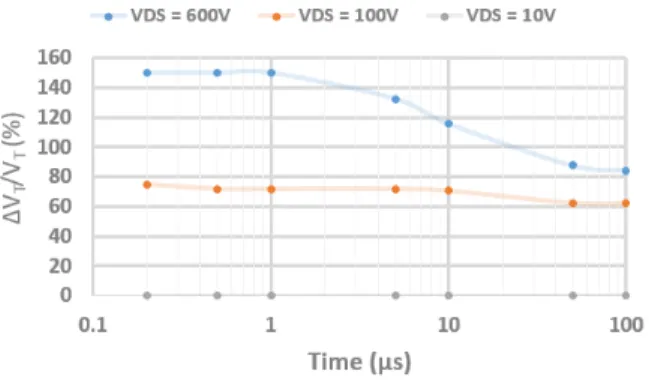
Figure 12 shows the evolution of the gate threshold voltage, extracted from GON(VGS) after a 1 s
drain-source stress of 100 V and 600 V, compared to the gate threshold obtained by classical static measurement (red curve Figures 10 and 11). After a high voltage stress, it appears that the dynamic gate-source voltage needed for the component to turn-on is far from the gate threshold given by a static measurement (up to 150 %).
Figure 12: Gate threshold variations due to voltage stress on the drain, compared to gate threshold obtained by classical static measurement
Conclusion
In GaN HEMT components, for low drain-source voltage (low trapping), the gate threshold value extracted from static measurement is close to the gate-source voltage leading to the switch-on of the component, whereas, for a high drain-source voltage (trapping), the gate threshold value extracted from static measurement appears to be different from the gate-source voltage leading to the switch-on of the component. So, because of traps in GaN materials, it seems that, in the applications and for analytical modeling, a special care has to be taken with the threshold voltage given by static tests.
References
[1] Zhou Xing-Ye, Feng Zhi-Hong, Wang Yuan-Gang, Gu Guo-Dong, Song Xu-Bo and Cai Shu-Jun, “Transient simulation and analysis of current collapse due to trapping effects in AlGaN/GaN high-electron-mobility transistor”, Chinese Physics B, volume 24, number 4,pages 048503, 2015.
[2] Liao, Wen-Chia, Chen, Cheng-Hsin, Hsu, Chia-Wei Hsin, Yue-Ming, Chyi, Jen-Inn, “Analysis of Threshold Voltage Shift in AlGaN/GaN Heterostructure Field-Effect Transistors with Different Buffer Layers”, Journal of The Electrochemical Society, vol. 162, N°8, January 2015.
[3] J. Joh, J.A. del Alamo, J. Jimenez, “A Simple Current Collapse Measurement Technique for GaN High-Electron Mobility Transistors”, Electron Device Letters, IEEE, vol. 29, N°7, pp. 665-667, July 2008.