Analyzing Sampling Methodologies in Semiconductor Manufacturing by
Richard M. Anthony
Bachelor of Science in Mechanical Engineering Purdue University, 1994
Submitted to the Sloan School of Management and the Department of Mechanical Engineering in Partial Fulfillment of the Requirements for the Degrees of
Master of Business Administration and
Master of Science in Mechanical Engineering
In Conjunction with the Leaders for Manufacturing Program at the Massachusetts Institute of Technology
June 2004
@ 2004 Massachusetts sti te (fTechnology./All rights reserved.
Signature of Author '
(Sloan School of Management Departm t of Mechanical Engineering May 7, 2004
Certified by
Sara L. Beckman, Thesis Advisor Senior Lecturer Haas School of Business, University of California, Berkeley Certified by
David E. Hardt, Thesis Advisor Professor of Mechanical Engineering, Department of Mechanical Engineering
Reviewed by
Donald B. Rosenfield, Thesis Reader Director, Leaders for Manufacturing Program Senior Lecturer, Sloan School of Management
Accepted by
Margaret C. Andrews, Executive Director of Masters Program Sloan School of Management
Accepted by
Ain Sonir djtif!tommittee
MASSACHUSETTS INS rUTE. Department of Mechanical Engineering OF TECHNOLOGY
JUL
0
1
2004
BARKE~R
Analyzing Sampling Methodologies in Semiconductor Manufacturing by
Richard M. Anthony
Submitted to the Sloan School of Management
and the Department of Mechanical Engineering on May 7, 2004 in Partial Fulfillment of the Requirements for the Degrees of
Master of Business Administration
and Master of Science in Mechanical Engineering ABSTRACT
This thesis describes work completed during an internship assignment at Intel Corporation's process development and wafer fabrication manufacturing facility in Santa Clara, California. At the highest level, this work relates to the importance of adequately creating and maintaining data within IT solutions in order to receive the full business benefit expected through the use of these systems.
More specifically, the project uses, as a case example, the sampling methodology used in the fab for metrology data collection to show that significant issues exist relating to the software application database and business processes concerning data accuracy and completeness. The organizational challenges contributing to this problem will also be discussed.
Various recommendations were undertaken to improve the application's effectiveness. As part of this effort, plans for an online reporting tool were developed allowing much greater visibility into the system's ongoing performance. Initial data updates and other improvements resulted in a reduction in both product cycle times and required labor hours for metrology operations.
Without a rigorous focus on the accuracy and completeness of data within manufacturing execution systems, the results of continuous improvement activities will be less than expected. Furthermore, sharing information relating to these projects across geographical boundaries and business units is vital to the success of manufacturing organizations. Thesis Supervisors:
Sara L. Beckman
Senior Lecturer, Haas School of Business, University of California, Berkeley David E. Hardt
Professor of Mechanical Engineering, Department of Mechanical Engineering Thesis Reader:
Donald B. Rosenfield
Director, Leaders for Manufacturing Program Senior Lecturer, Sloan School of Management
3-ACKNOWLEDGEMENTS
I would like to thank the numerous co-workers, friends, and family members that have supported me during these last two years:
In particular, I would like to acknowledge the Leaders for Manufacturing program, a partnership between the Massachusetts Institute of Technology and major manufacturing partners, and the program's supporters for providing this opportunity for study at MIT. I
would also like to thank my LFM classmates for helping to create a very unique learning environment.
I would like to give special recognition to my supporters and sponsors at Dell, especially Stephen Cook, John Egan, and Dick Hunter. I am very grateful for this wonderful
opportunity and look forward to my continued career at Dell.
I would like to thank my thesis advisors, Sara Beckman and Dave Hardt, for their patience, guidance, and support during the internship and thesis writing experience. I would like to extend my gratitude to Intel Corporation and employees at the D2 manufacturing facility for giving me the opportunity to carry out this work. Special thanks go to my sponsors, Chris Keith and Erik Stewart, and the entire Manufacturing Systems Engineering group (David Auchard, Hyung Kang, Joe McMorrow, and Chris Mullendore) for welcoming me into the group. I would also like to give my appreciation to John Powell for his advice and mentoring and Alan Wong for his active involvement
during the project.
Most importantly, this work is dedicated to my wife, Michelle, and my daughter, Molly.
Without their love, 'encouragement, and sacrifices this two-year adventure would not
have been possible!
-5-TABLE OF CONTENTS
Abstract...3
Acknow ledgem ents ... 5....5
Table of C ontents ... 7
Table of Figures...9
Table of T ables ... ... 9
Chapter 1 - Introduction & Overview ... 11
1.1 Project Overview ... 11
1.2 Project M otivation ... 12
1.3 O rganization of the Thesis ... 12
Chapter 2 - Project Background & Description...15
2.1 Intel Corporation Overview ... 15
2.1.1 Intel Operations... 16
2.1.2 Supply Chain Perspective for Semiconductor Manufacturing... 17
2.2 Technology D evelopm ent... 18
2.2.1 The Different Phases of Semiconductor Manufacturing ... 18
2.2.2 California Technology M anufacturing ... 19
2.2.3 D2 Charter... 19
2.3 A Changing M arket...20
2.3.1 Intel Aggressively Enters the High Mix, Low Volume Market... 20
2.3.2 Challenges of High Mix, Low Volume Manufacturing... 21
2.3.3 HM LV Sum m ary ... 22
Chapter 3 - Semiconductor Manufacturing and Metrology ... 23
3.1 Sem iconductor M anufacturing... 23
3.1.1 M anufacturing Overview ... 23
3.1.2 W afer Fabrication Processes and Equipm ent ... 24
3.2 Sem iconductor M etrology ... 26
3.2.1 Photolithography (Litho) M etrology... 27
3.2.2 Defect M etrology ... 28
Chapter 4 - Sam pling Plans...31
4.1 A cceptance Sam pling... 31
4.2 Lot-by-lot A cceptance Sam pling by Attributes ... 32
4.2.1 Dodge-Rom ig Sam pling Plans... 33
4.2.2 Single Sam pling Plan... 33
4.2.3 Double Sam pling Plan ... 33
4.2.4 M ultiple Sampling Plan ... 34
4.2.5 Switching Procedures between Normal, Tightened, and Reduced Inspection ... 34
4.3 A cceptance Sam pling by Variables... 35
-7-4.4 Continuous Sam pling Plans ... 36
4.4.1 The First Continuous Sampling Plan, CSP-1... 36
4.4.2 Continuous Sam pling Plans, CSP-2 & CSP-3... 36
4.4.3 Additional Continuous Sampling Plans ... 38
4.5 Skip Lot Sam pling Plans...38
4.6 Intel's Sam pling Process...40
4.6.1 The SkipLot5 Application... 41
4.6.2 The M OST M odel... 44
Chapter 5 - Q uality Audit... 47
5.1 W hat is a Quality Audit?... 47
5.2 Analysis of the SkipLot5 System ... 48
5.2.1 Process for the D2 M easurem ent Rate Analysis... 48
5.2.2 M easurem ent Rate Analysis Results Summ ary ... 51
5.3 SkipLot5 System Quality Audit Overview ... 54
5.3.1 System Design ... 54
5.3.2 Business Processes... 55
5.3.3 Ownership ... 56
5.3.4 Visibility into System 's Perform ance ... 56
5.4 Transient D ata Study... 57
5.4.1 Current Practices ... 57
5.4.2 The Group Short Run Individual X and Moving Range Control Chart... 58
5.4.3 Interpretation of the Results... 60
Chapter 6 - O rganizational Change ... 65
6.1 Strategic Design Lens ... 65
6.1.1 Organizational Strategy ... 65 6.1.2 Organizational N eeds... 66 6.1.3 Organizational Structure ... 66 6.1.4 Necessary Changes ... 67 6.2 Political Lens ... 67 6.2.1 Stakeholder Analysis ... 67
6.2.2 Conflicts and Resolution... 69
6.3 Cultural Lens...69
6.3.1 Reinforcement of Norms, Values, and Basic Assumptions... 69
6.3.2 Inform ation Sharing ... 70
Chapter 7 - Recommendations and Concluding Remarks...73
7.1 Recom m endations... 73
7.1.1 Short-Term Recom m endations ... 73
7.1.2 Long-Term Recom m endations ... 74
7.2 Future Project Opportunity ... 75
7.3 Concluding Rem arks... 76
7.4 Conclusion ... 79
TABLE OF FIGURES
Figure 2.1: Semiconductor Manufacturing Supply Chain at Intel... 17
Figure 2.2: Different Phases of Semiconductor Manufacturing. ... 18
Figure 3.1: Representation of a Typical Semiconductor Fabrication Line... 23
Figure 3.2: Re-entrant Nature of Semiconductor Processing. ... 24
Figure 3.3: Examples of (a) Translation, (b) Rotation, and (c) Magnification Defects... 28
Figure 3.4: Examples of Particulate (a & b) and Missing Pattern (c & d) Defects... 29
Figure 4.1: Switching Rules for Normal, Tightened, and Reduced Inspection. ... 35
Figure 4.2: Alternating Periods of 100% Inspection and Sampling, CSP-1... 36
Figure 4.3: CSP-2 Sampling Procedure. ... 37
Figure 4.4: The Basic Structure of a Skip Lot System... 39
Figure 5.1: Analysis Results in Terms of Potential Cycle Time Savings... 52
Figure 5.2: Analysis Results in Terms of Potential Labor Savings. ... 54
Figure 5.3: The Control Chart Decision Tree. ... 59
Figure 5.4: Group Short Run Individual X Chart. ... 61
Figure 5.5: Group Short Run Moving Range Chart... 62
Figure 6.1: The Three Lenses. ... 65
Figure 6.2: Stakeholder M ap... 68
Figure 7.1: Schematic of Intel's Fab Manufacturing Execution Systems... 78
TABLE OF TABLES Table 3.1: Semiconductor Equipment Types and Applications... 26
Table 4.1: Sample SkipLot5 Test Type Data Table... 43
Table 4.2: Sample SkipLot5 Decision Point Data Table. ... 44
Table 5.1: Simplified Measurement Rate Analysis... 50
-9-CHAPTER 1 - INTRODUCTION & OVERVIEW 1.1 Project Overview
Many manufacturing companies are dealing with rapidly changing markets and industries. The most successful ones will be those that can deliver new and improved products to the customers at a faster pace than the competition - at a profit. Typically, manufacturing execution systems, necessary to keep pace with the industry's changing landscape, are weighted down by their own complexities causing great difficulties during their implementation or modification. This situation is especially true for those industries where product life cycles are getting shorter and the variety and complexity of the products are increasing.
"While U.S. manufacturers recognize the importance of speed and flexibility, many are impeded by efforts to become more agile producers. Even highly automated plants and factories struggle to overcome difficulties in adapting or reconfiguring production operations to accommodate design changes and new product lines. Idiosyncrasies in manufacturing software and incompatibilities among software applications are a primary source of costly delays..." 2
This thesis deals with these issues at a high level while using one particular example as a case study. The project undertaken at Intel's process development and semiconductor fabrication facility in Santa Clara, California involves the information technology application for their sampling methodology used for metrology data collection. Several issues exist with the accuracy and completeness of data due to the system design, organizational structure, and business processes. Each one of these will be discussed in later chapters.
Christopher, Neil. National Institute of Standards and Technology. Technologies for the Integration of Manufacturing Applications (TIMA). 22 May 2003. 17 Mar. 2004'
<http://www.atp.nist.gov/www/press/9705tima.htm>. 2 ibid
-1.2 Project Motivation
This project was motivated by the desire to improve one of the high mix, low volume challenges discussed in Chapter 2 - increased inspection requirements. Early in the internship assignment, it came to management's attention that the measurement rates for specific products at metrology operations were much higher than expected. Therefore, it was believed that by studying the data, systems, and business processes inherent to Intel's sampling methodology, improvements could be made to reduce the impact that the increased number of measurements caused by an increased product mix will have on D2's labor requirements and cycle time.
1.3 Organization of the Thesis
This paper is divided into six subsequent chapters.
Chapter 2 discusses Intel Corporation, its products, and its latest strategy for entry into the demanding consumer electronics business. The technology development activities of semiconductor manufacturing at Intel are discussed with a review of the organization where the project work was completed.
Chapter 3 briefly reviews the complex semiconductor manufacturing processes in order to present these to a reader new to the topic. Metrology operations are then introduced providing special attention to those metrology areas studied during the project. Chapter 4 reviews widely accepted sampling plans and, more importantly, Intel's current practices and application of their skip lot sampling methodology.
Chapter 5 begins with a discussion of a quality audit and includes a detailed system analysis of Intel's skip lot sampling plan. It presents the outcome of a quality review -for this system, focusing on perceived versus actual measurement rates and includes a special study of transient data resulting from bringing equipment online after downtime events. This allows a comparison of the results of the analysis to actions taken
in the fab. Finally, it reviews a reporting tool to improve the accessibility and availability of measurement rate data in the future.
Chapter 6 provides a cultural perspective on the above issues and the internship assignment, in particular.
Finally, Chapter 7 includes specific recommendations for improvement, the implementation status, a possible future project, and general observations regarding the flow of information within and across organizations.
-CHAPTER 2 - PROJECT BACKGROUND & DESCRIPTION
This chapter outlines details regarding Intel Corporation including its products,
basic strategy for continued growth, and manufacturing operations as well as background materials specific to the project. This sets the stage for further chapters discussing
quality assurance and sampling plans at the D2 research and development semiconductor wafer fabrication facility.
2.1 Intel Corporation Overview
Intel is the world's largest semiconductor chip manufacturer and holds a
commanding lead over its nearest competitors with an estimated 80% share of the
worldwide microprocessor market.3 Fiscal year sales were just over $30 Billion with net income exceeding $5.6 Billion due to gross profit margins over 60%.4
The company's primary focus is to design, develop, manufacture, and market computing, networking, and communication products with the following corporate mission:
"Do a great job for our customers, employees and stockholders by
being the Nreeminent building block supplier to the worldwide Internet
economy."
Intel's major product categories include microprocessors, chipsets, motherboards,
wired and wireless connectivity products, flash memory, and both processors and chipsets for the cellular and handheld computing industries. At the end of 2003, the corporation was divided into three primary business units: Intel Architecture, Intel Communications Group (ICG), and the Wireless Communications and Computing Group (WCCG). Each segment works to develop improved integrated circuits and silicon
solutions in support of the corporate goal.
3 Carbone, Jim. "Microprocessors Show Signs of Life as Demand Builds." Purchasing. 20 Nov. 2003: 17-18. Business Source Elite. EBSCOhost. 15 Mar. 2004. Keyword: Intel market share.
4 Edelstone, Mark L. (4 Mar. 2004). Intel Corp. Fine-Tuning EPS Estimate Lower. Equity Research Note. Morgan Stanley. Retrieved 15 Mar 2004 from InvestText Plus Database.
5 Intel Corporation. "From Silicon to Software." Intel's Quality System Handbook, 15 Mar. 2004 <http://developer.intel.com/design/quality/quality.htm>.
-The Intel Architecture organization accounted for roughly 87% of the company's revenues in 2003 - 73% specifically from the microprocessor business. Within this group, technology solutions are developed using its microprocessor, motherboard, and chipset capabilities for the personal computing and server markets. The Intel Communications Group and Wireless Communications and Computing Group accounted for 7% and 6% of consolidated 2003 net revenues, respectively.6
2.1.1 Intel Operations
The Technology and Manufacturing Group (TMG) is responsible for all of Intel's manufacturing operations and technology development activities worldwide. Manufacturing facilities are located in the United States, Israel, Ireland, Malaysia, the Philippines, China, and Costa Rica.
Fab Sort Manufacturing (FSM) and Assembly Test Manufacturing (ATM) report to TMG as well as several other organizations in charge of technology development, system manufacturing, and other support services. Fab Sort Manufacturing is responsible for Intel's wafer fabrication and sort facilities while Assembly Test Manufacturing controls the remaining activities of assembly and final test.
Each fab is assigned a set of products requiring various technologies and processes that it will manufacture based on the limitations and utilization of its existing equipment. For instance, Fab A may be dedicated to certain flash memory products while Fabs B and C utilize their resources to produce various microprocessor products. This would result in Fabs B and C being part of the logic "virtual factory" since they manufacture the same or similar (logic) products. The results of yield and output improvement projects are shared among all members of the "virtual factory" after being implemented at one facility. Within this "virtual factory" framework, changes to processes and equipment at all manufacturing sites are tightly controlled to ensure each
6 Intel Corporation. (27 Dec 2003). "Form 10-K." Annual Filing with the United States Securities and Exchange Commission, Retrieved 10 Mar 2004, from Thomson Research Database.
facility is as similar to the others for resource sharing, benchmarking, improved yield learning, increased speed to capacity ramp, and optimal manufacturing flexibility.7
2.1.2 Supply Chain Perspective for Semiconductor Manufacturing
In order to convert silicon into packaged electronic components, four basic factory operations are necessary: wafer fabrication, wafer sort, packaged component assembly, and final test (reference Figure 2.1). Intel uses a die bank (an inventory of fabricated and cut wafers) as an interface between their push-based strategy (wafer fab and sort) and their pull-based strategy (assembly and final test).
Working Devices
Bare Silicon
->Wafer-Fab Wafer Sort
Wafers PL
B
Fab Sort Manufacturing
Components
Assembly Final Test
ash - Pull Packaged
oundary Devices
Assembly Test Manufacturing
Figure 2.1: Semiconductor Manufacturing Supply Chain at Intel.
Within the wafer sort operation, each die (or microprocessor chip) on completed wafers is tested for functionality and performance. These wafers are then cut to separate the individual chips and sorted based on the test results. The good chips are sent to the die bank for future retrieval by assembly operations. Packaged devices are the result of the assembly process where individual die are mounted and prepared for use in customer applications. Prior to shipment, each one of these packaged microprocessors is tested again for functionality and performance in the final test operation.
7 Ponchner, Karen. "Implementing Advanced Process Control in a Copy EXACTLY! Environment." Thesis. Massachusetts Institute of Technology, 2002. 24-26.
' Adapted from Atherton, Linda F., and Robert W. Atherton. Wafer Fabrication: Factory Performance and Analysis. Boston: Kluwer Academic, 1995. 6.
-2.2 Technology Development
This section discusses the different phases of semiconductor manufacturing including technology development. Specifically, the charter of Intel's California Technology Manufacturing D2 organization is explained to describe the context for this thesis project.
2.2.1 The Different Phases of Semiconductor Manufacturing
Yield management is critical to the success of a wafer fab. The yield learning cycle varies significantly between the different phases of semiconductor manufacturing. Figure 2.2 represents the expectations for yield improvements between these different phases: exploratory research and development, process development, yield learning during manufacturing ramp, and yield monitoring of a stable manufacturing process.
systematic + random
random yield
yield loss
loss
00 0E
00
S
Figure 2.2: Different Phases of Semiconductor Manufacturing.9
During the first stage of research and development, relatively few measurements are taken for quality assurance since the primary purpose of this timeframe is to determine product feasibility through experiments. As the product progresses through the
9 Diebold, Alain C., ed. Handbook of Silicon Semiconductor Metrology. New York: Marcel Dekker, Inc.,
process development phase into manufacturing ramp, measurements and data collection processes are critical to maximize opportunities for yield learning. For this reason, data collection procedures are typically automated to gather the necessary information for improving yield. The number of measurements taken and time invested in metrology are at a maximum during this phase. The inspection process has a critical role in improving fab yield and cost effectiveness at this time by enabling both the early discovery of defects and the corrective action necessary to avoid similar mistakes. At this point in the manufacturing process maturity, additional inspections lead to fewer defects and higher yields. Finally, when the manufacturing processes mature and stabilize, the number of measurements needed to maintain optimized levels of yield is reduced for cost reasons.
2.2.2 California Technology Manufacturing
During the process development phase, Intel uses technology development (TD) organizations to define the manufacturing processes prior to transferring the products and processes to high volume manufacturing fabs. One of these groups is California Technology Manufacturing (CTM) located in Santa Clara, California. CTM includes Intel's 200 mm process development wafer fab, known as D2, where this thesis work was performed. The following section describes D2's primary purpose and role within Intel and CTM.
2.2.3 D2 Charter
The D2 wafer fab has a vision to deliver leading edge silicon processes to accelerate and broaden Intel's competitive leadership. In order to do this, their charter has three distinct goals:
* Develop process technologies
* Ensure successful transfers of new technologies to the virtual factory
0 Maintain a stable manufacturing base for rapid deployment of the new products and process technologies to the virtual factory
D2 is one of the few Intel fabs focused on both high volume manufacturing and technology development for new processes. As a production facility, it joins the virtual
-factory's attempts to improve yield learning while also helping to fulfill production volume requirements. Because of its dual purpose, there is an important need for resources to focus on the high mix, low volume challenges discussed in the next section. 2.3 A Changing Market
Over the last several years a gradual shift has been realized for an ever-increasing demand of flash products and more variations to the memory product family.
2.3.1 Intel Aggressively Enters the High Mix, Low Volume Market
Worldwide chip sales are projected to increase by 25% in 200410 due to the rising popularity of consumer electronic devices such as cellular phones, flat panel televisions, portable music and video players, and wireless home networking. With this surge of increased demand for digital content, the chip designers and manufacturers are placing a high priority on product development projects to enter this business. Business Week magazine reports that Walden Rhines, the CEO of chip design software maker Mentor Graphics, "expects chip companies to create 20% to 50% more new versions during the current upturn than in past recoveries."" Product development for these new markets is focused on the following four key areas:
" Finding ways to include more functionality onto smaller chips " Capturing additional market opportunities with improved packaging
* Identifying new types of integrated circuitry * Improving materials and manufacturing processes
Craig Barrett, Intel's CEO, has created a new plan to include Intel chips in every digital product available on the market. This corporate strategy has been tagged the "Intel Everywhere" plan by Business Week in contrast to the previous "Intel Inside"
1O Kharif, Olga. "A Whole New World of Chips." Business Week Online 21 Jan. 2004. 13 Mar. 2004 <http://www.businessweek.com/technology/content/jan2004/tc20040121_4923_tcl 39.htm>.
marketing campaign.12 "Barrett fully intends to upend the status quo in communications
and consumer electronics markets. Think of Intel as the silicon arms dealer."13
To meet this challenge, new products for the communications markets are being developed by Intel's research and development fabs. There is "a lot more variety [in chips] than there has ever been," quotes Business Week of Brian Matas, an analyst for the semiconductor consulting firm IC Insights.14 Due to the types and numerous markets
ready for entry, each of these new product variations will ultimately be produced in lower volumes than the typical Intel Architecture microprocessor product family. This has and will continue to force Intel's manufacturing environments to deal with a higher mix of products at lower volumes.
2.3.2 Challenges of High Mix, Low Volume Manufacturing
As suggested by the product-process matrix described by Hayes and Wheelwright15 in 1979, it would be difficult to simply assign high mix, low volume
products to Intel's existing high volume manufacturing facilities. This situation requires an analysis of the manufacturing characteristics required to efficiently run a high mix, low volume manufacturing environment. Some of the many problems an existing high volume semiconductor manufacturing facility would encounter when producing components of a high mix in lower volumes are listed below.'6
* Reduced yield - High volume fabs allow benefits to be gained and improvements to be made over time as learning occurs. When a facility is forced to run a lower volume of many more products, this learning effect cannot be realized (through repetition of running the exact same product over and over) in order to
significantly improve the product yield.
12 Edwards, Cliff, Moon Ihlwan, and Andy Reinhardt. "What is CEO Craig Barrett Up To? Hint: It's About
Much More than Computers." Business Week Online 8 Mar. 2004. 10 Mar. 2004 <http://www.businessweek.com/magazine/content/04_10/b3873001_mzOOl.htm>.
" ibid
1" Kharif, Olga. "Memory: Beyond Flash and DRAM." Business Week Online 21 Jan. 2004. 14 Mar. 2004
<http://www.businessweek.com/technology/content/jan2004/tc20040121_9640_tcl39.htm>.
1 Hayes, Robert, and Steven Wheelwright. "Link Manufacturing Process and Product Life Cycles."
Harvard Business Review 1979.
16 Scholtz III, Robert L. "Strategies for Manufacturing Low Volume Semiconductor Products in a High
Volume Manufacturing Environment." Thesis. Massachusetts Institute of Technology, 2002. 10-11.
-21-* Increased inspection requirements - These low volume products require an increased level of inspection to ensure a high quality product is delivered to the customer.
" Increased setup costs - The higher mix of lower volume products requires extra setups to be performed taking away valuable equipment utilization time.
" Increased number of new product introductions - The new product introduction (NPI) process is designed to optimize the manufacturing environment for a given product when it is first produced at a new facility. This NPI process is time-consuming and resource intensive. With the large amount of products beginning to enter Intel's manufacturing facilities, many more NPIs will result than in recent history, demanding additional time and resources.
2.3.3 HMLV Summary
In summary, Intel has chosen a new strategy to aggressively enter the consumer electronic device and communications markets. Due to the nature of this new arena, several product variations, each of relatively low volume, will be required to meet customer demands. As a result, Intel is now faced with a high volume manufacturing organization that must learn to incorporate high mix, low volume products into its existing manufacturing infrastructure.
CHAPTER 3 - SEMICONDUCTOR MANUFACTURING AND METROLOGY This chapter introduces the manufacturing processes and complex nature of semiconductor wafer fabrication facilities followed by a review of semiconductor
metrology operations.
3.1 Semiconductor Manufacturing 3.1.1 Manufacturing Overview
Semiconductor manufacturing consists of a complex sequence of processes that build three-dimensional structures onto the surface of single-crystal silicon wafers. This
manufacturing process includes many processing steps where layers of various materials are deposited onto the wafer for specific reasons. Each layer is then patterned and connected to underlying layers. Figure 3.1 shows a schematic of the typical process flow.
WaferReticle Reticle
Generation < Generation Inspection
--Mask - - -- - - Making
Wafer Starts
Oxidize,
Sc rub & Deposit, Apply Expose
Dehydrate Gowor Photoresist Photoresist
Met allie :
Strip e s
Rapi
No
Wafer Electrical Inspect Chemical
Processing Process Optically Mechanical
Oomp>lete?a Diagnostics Polish
Yes
Wafer Finishes
Figure 3.1: Representation of a Typical Semiconductor Fabrication Line.17 " Adapted from Doering, Robert, and Yoshio Nishi, eds. Handbook of Semiconductor Manufacturing Technology. New York: Marcel Dekker, Inc., 2000. 25.
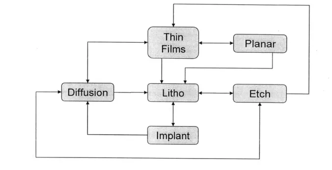
-A sequence of several hundred steps is necessary to complete this highly re-entrant manufacturing process. Figure 3.2 is a schematic of the re-re-entrant nature of a typical microprocessor product between the six major processing steps. These steps are discussed in more detail in the next section.
ns
Planar
Diffu sion
'LithoEtcah
Implant
Figure 3.2: Re-entrant Nature of Semiconductor Processing.'" 3.1.2 Wafer Fabrication Processes and Equipment
As indicated above, there are six primary processes involved with microprocessor production: diffusion, thin films, implant, photolithography (litho), etch, and planar. Each one of these is explained below.
0 Diffusion - In the diffusion area, wafers are heated in the presence of reactive
gases to grow layers on the wafer surface or un-reactive gases to "drive" implanted materials to their desired depth.
* Thin films - Thin films are deposited onto the wafer surface using chemical vapor
deposition, sputtering, or an electroplating process.
18 Adapted from Quirk, Michael, and Julian Serda. Semiconductor Manufacturing Technology. Upper
* Implant - In order for silicon to conduct electricity, impurities are implanted into the surface of the wafer by way of the ion implantation process.
" Litho - Patterns are printed onto masks (or reticles) which are then transferred to the wafer surface through the process of spinning resist onto the wafer, exposing the resist using the reticle, and developing the resist.
" Etch - Etching takes place in an acid bath (wet etch) or in an oxygen plasma environment (dry etch). This etching process removes the resist pattern from the wafer.
" Planar - During the planar or polishing steps, chemical and mechanical
processing of the wafer removes surface topography ensuring a smooth and flat surface for further processing.
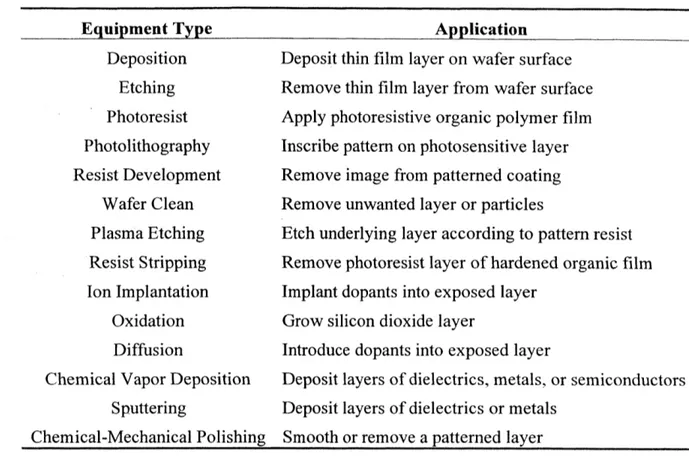
Semiconductor manufacturing is highly technical work accomplished by specialized equipment within a fabrication facility's clean room for minimum exposure to particulate contamination. In advanced fabs, as many as fifty different types of equipment may be necessary to complete this entire process. A brief summary of the major classifications of equipment types is shown in Table 3.1.
-Table 3.1: Semiconductor Equipment Types and Applications. 9
3.2 Semiconductor Metrology
Variations during the integrated circuit manufacturing process can result in defects in the semiconductor device's performance. At times, these product variations can result in dramatic reductions to a fab's yield. Therefore, manufacturing of integrated circuits includes metrology operations after each major processing step to improve the yield learning cycle (and ultimately, the fab's yield). These metrology steps verify that particle contamination is within certain parameters and product design requirements are
being met.
There are two main types of metrology operations studied during the course of this work at Intel's D2 process development wafer fab: photolithography (litho) metrology and defect metrology. Combined, these metrology operations account for roughly 30% of the total number of steps in the manufacturing sequence and 19 Atherton, Linda F., and Robert W. Atherton. Wafer Fabrication: Factory Performance and Analysis. Boston: Kluwer Academic, 1995. 7-9.
Equipment Type Deposition Etching Photoresist Photolithography Resist Development Wafer Clean Plasma Etching Resist Stripping Ion Implantation Oxidation Diffusion
Chemical Vapor Deposition Sputtering
Chemical-Mechanical Polishing
Application Deposit thin film layer on wafer surface Remove thin film layer from wafer surface Apply photoresistive organic polymer film Inscribe pattern on photosensitive layer Remove image from patterned coating Remove unwanted layer or particles
Etch underlying layer according to pattern resist Remove photoresist layer of hardened organic film Implant dopants into exposed layer
Grow silicon dioxide layer
Introduce dopants into exposed layer
Deposit layers of dielectrics, metals, or semiconductors Deposit layers of dielectrics or metals
approximately 39% of the cycle time required to complete the semiconductor device.2 The different types of metrology operations are briefly described in the next two sections. 3.2.1 Photolithography (Litho) Metrology
After the value-add processing step is completed for each litho layer, various problems are identified through four types of metrology operations: macro inspect, develop check, critical dimension verification, and image placement. For most products and layers, all four of these metrology operations are completed resulting in numerous occasions where manufacturing technicians handle the wafers checking for different defect types.
* Macro inspect - During this operation, a metrology technician uses special equipment to rotate the wafer under a monochromatic light to visually detect easily identifiable issues (at the macro level) resulting from the resist processing steps.
* Develop check - An optical microscope is used for the develop check operation to inspect wafers for resist pattern defects or other anomalies only visible under magnification.
* Critical dimension verification - A scanning electron microscope (SEM) is used to measure the critical dimensions of pre-defined features to verify they are within product parameters.
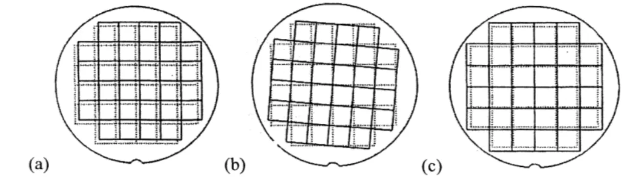
* Image placement - This step (known as registration) determines the amount of overlay between the current layer and an alignment layer underneath. Three
common errors are shown in Figure 3.3.
20 Data taken from a typical product (P8xB) manufactured at D2 in December 2003.
-27-(a) (b) (c)
Figure 3.3: Examples of (a) Translation, (b) Rotation, and (c) Magnification Defects.2 1
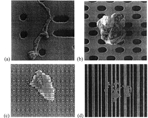
3.2.2 Defect Metrology
Litho metrology involves identification of errors specifically associated with the photolithography processes such as spinning resist onto the wafer, exposing the resist
using the reticle, and developing the resist. This second major classification of metrology, defect metrology, deals with other types of defects that negatively impact product value or functionality leading to lost revenue. These defects can be particles or other imperfections on the wafer that are not intended to be there or any feature missing from the wafer. These defects need to be located as early as possible during the
manufacturing process allowing for fewer wafers to be affected, a faster feedback loop
for problem resolution, and a lower cost of production.
Typically, either an optical microscope or a SEM would be used to initially
inspect wafers and locate the existence of defects such as those shown in Figure 3.4. Defect review tools are also used to further inspect and characterize the nature of unknown material enabling the root cause of the defect to be isolated and contained. The
equipment used for defect review is similar to the optical microscopes and SEMs.
However, the purpose of their use is to verify that a "detected" defect truly exists and to
provide for element classification.
Doering, Robert, and Yoshio Nishi, eds. Handbook of Semiconductor Manufacturing Technology. New York: Marcel Dekker, Inc., 2000.
(a) (b)
(c) (d)
Figure 3.4: Examples of Particulate (a & b) and Missing Pattern (c & d) Defects..
22 Diebold, Alain C., ed. Handbook of Silicon Semiconductor Metrology. New York: Marcel Dekker, Inc.,
2001.693.
-CHAPTER 4 - SAMPLING PLANS
The previous chapter presented an overview of semiconductor manufacturing, its complexities, and typical metrology operations necessary to improve yield learning. This chapter deals specifically with different methods to gather the inspection data while also reducing the impacts these activities have on manufacturing costs and productivity.
4.1 Acceptance Sampling
There are three approaches to the decision-making process regarding product lot
quality:2 3
0 Accept lots without any form of inspection
* Inspect all lots and remove, rework, or replace defective units 0 Implement the use of acceptance sampling for lot quality review
Accepting lots without inspection would typically only be done for those
processes that have been consistently proven to be in control over a long period of time.
At the other end of the spectrum, all lots may be inspected in those cases where critical
product features must be tightly controlled or when the process capability is inadequate to meet specifications. In between, acceptance sampling may be used for the following
types of situations:24
* When the testing procedure is destructive - making 100% inspection clearly impractical
" When the costs of 100% inspection are relatively high
0 When the inspection and analysis process takes a relatively long period of time * When a reduction from 100% inspection is desired, but the process capability
does not warrant zero inspections.
* When product liability justifies continuous monitoring
23 Montgomery, Douglas C. Introduction to Statistical Quality Control. New York: John Wiley & Sons, 1985. 351-354.
24 ibid
-Intel semiconductor metrology operations fall into the third and fourth categories above. A large amount of time is necessary for some test results to be returned to the technician who is making processing decisions (e.g. continue running the batch under current conditions or tweak the equipment settings to produce a better product). This can result in unwanted equipment idle time adversely affecting fab capacity, cycle time, and costs. Furthermore, due to the increasing shift towards high mix, low volume manufacturing, discussed in chapter 2, efforts have been initiated to reduce the quantity of measurements taken throughout the manufacturing process while still requiring some form of ongoing -monitoring.
Many advantages to acceptance sampling plans exist when compared to 100% inspection plans. These include a decreased number of inspections resulting in lower production costs, less metrology labor involvement, and less product manipulation where unnecessary product damage could result. However, there is also an increased opportunity for accepting "bad" lots and rejecting "good" lots. Another disadvantage is that the learning cycle gained from the data collected during the inspection process is
slowed due to the reduced number of measurements.
Therefore, the key to gathering data is to do so frequently enough that process changes are captured but not so often that the activity of data collection and analysis is too expensive to be useful. Many different types of inspection methodologies are used within manufacturing operations for the purpose of accepting or rejecting product based on adherence to a standard. Some of the more common acceptance sampling methods are described in the following sections for the purpose of providing context for Intel's acceptance sampling system.
4.2 Lot-by-lot Acceptance Sampling by Attributes
This section explains various types of lot-by-lot acceptance sampling plans using attribute data to classify items as either defective or non-defective based on pass/fail conditions.
4.2.1 Dodge-Romig Sampling Plans
Two types of sampling plans were developed by H. F. Dodge and H. G. Romig that use a set of sampling inspection tables specifically for lot-by-lot inspection: lot tolerance percent defective (LTPD) and average outgoing quality limit (AOQL). The LTPD sampling plan provides protection for the downstream customer in that it involves a risk no greater than the specified amount of accepting any given lot of unsatisfactory quality. AOQL sampling plans are designed for those situations where there is little interest in the quality level of individual lots. Here, protection is provided to the customer in terms of the average outgoing quality for the product over a series of lots.25 Both of these systems can be developed with the single and double sampling procedures explained in the following sections.
4.2.2 Single Sampling Plan
A single sampling plan is a decision-making process where one sample of n units is randomly chosen from a given lot. An acceptance number c is used to determine the disposition of the entire lot. If more than c defective items are found in the sample, the lot is rejected. Otherwise, the entire lot is accepted for further processing or delivery to a customer.
4.2.3 Double Sampling Plan
A double sampling plan is similar with additional complications. After the initial sample is evaluated, the entire lot is accepted, rejected, or submitted for a second sample. In those cases where a second sample is necessary, the information from both samples is used to disposition the lot. The parameters that define this type of sampling plan are a
sample size for the first and second samples (n, and n2), an acceptance number for the first sample (ci), and an acceptance number for the combined samples (c2).
If the number of defects observed in the first sample (di) is less than cl, then the lot is accepted. The lot is rejected if d exceeds C2. In those situations where d, is
between c1 and C2, a second random sample of size n2 is required. At this point, the lot is 25 Dodge, Harold F. "Notes on the Evolution of Acceptance Sampling." American Society for Quality Control (1973).
-33-accepted if the combined number of defects observed in both samples (d, + d2) is less
than c2 and rejected if it is larger than c2.
4.2.4 Multiple Sampling Plan
A multiple sampling plan is similar to the double-sampling plan except in the case where more than two samples may be necessary to disposition a given lot. After any stage of the sampling process, if the number of total defects observed (I d, ) is less than or equal to the acceptance number for that particular stage (cj), then the lot is accepted. The lot is rejected after any stage of sampling if the total number of defects observed is greater than the acceptance number for that stage. If neither situation occurs, then sampling continues until all stages of sampling are satisfied.
This sampling method is complex to implement but can result in cost savings associated with the sampling process since the sample sizes are typically smaller than single or double sampling plans.
4.2.5 Switching Procedures between Normal, Tightened, and Reduced Inspection Military standard 105D (or the civilian equivalent ANSI/ASQC ZI.4) provides for different inspection levels based on the specified acceptable quality level (AQL). Normal inspection is used at the start of the measurement activity and under normal conditions where the manufacturing process is producing acceptable results. Tightened inspection levels are required when quality degrades. Reduced inspection can be implemented with exceptionally good product quality.
Start -Production is
steady 2 out of 5
10 consecutive consecutive
ots accepted lots rejected
"and" conditions Reduced iNormal l hanes d - Lot rejected t s cynethes - irregular production d t otgmep (9d
V a Other conditions th
warrant return to 10 consecutive
normal w lots remain on
tightened inspection
Corctive nl
tol N equired Figure 4.1: Switching Rules for Normal, Tightened, and Reduced Inspection.
The criteria specified in Figure 4.1 are used to determine whether or not it is appropriate to switch from one state to another. For example, when the inspection process is operating under tightened conditions, the observation of five consecutive acceptable lots allows a switch to the normal operating conditions. The difference between normal, tightened, and reduced inspection. conditions involves changes to the lot size (n) and acceptance number (c). Full tables specifying these various inspection systems are available in MIL-STD 105D and reprinted in Montgomery (1985).
4.3 Acceptance Sampling by Variables
Variables sampling plans specify the product to be sampled and the criteria for decision-making using measurements to identify the quality characteristics of certain product features. Typically, this is accomplished based on the sample average and sample -standard deviation where lot acceptance depends on the sample average in relation to the upper or lower specification limit.
26 Adapted from Montgomery, Douglas C. Introduction to Statistical Quality Control. New York: John
Wiley & Sons, 1985.
-4.4 Continuous Sampling Plans
In some manufacturing environments, the natural formation of lots does not exist. Therefore, sampling plans involving continuous sampling versus lot sampling are used for processes consisting of a nearly continuous flow of products. Several different plans of this type are presented below.
4.4.1 The First Continuous Sampling Plan, CSP-1
The CSP-I plan specifies a clearing interval (i) and a sampling frequency (f). The process includes intervals of 100% inspection alternating with periods of random sampling from the continuous flow of products. During the 100% inspection period, once i consecutive units are found to be free from defects, random sampling at the rate of frequency
f
begins. When a defect is identified at any point during the sampling stage, 100% inspection resumes. Figure 4.2 shows these alternating periods of 100% inspection and acceptance sampling.100% Inspection Sampling 100% Inspection Sampling
+OCOSCD tCOOO O 0 0 0 . .. 0 0 0 0 0 00+ C 0 O 0X0 0 000 +
+
Defective Units0 Good Units
Figure 4.2: Alternating Periods of 100% Inspection and Sampling, CSP-1.2 7
4.4.2 Continuous Sampling Plans, CSP-2 & CSP-3
The CSP-1 acceptance sampling plan explained above requires the return to 100% inspection for any defect identified within the sample. This is equivalent to an acceptance number (c) equal to zero in a single sampling plan. However, it may not always be necessary to take action (such as returning to 100% inspection) when a defect is found. The CSP-2 and CSP-3 plans were developed for these situations.
27 Dodge, Harold F. "Notes on the Evolution of Acceptance Sampling." American Society for Quality
Another parameter called the clearing interval (k) is added which allows for sampling to continue as long as multiple defects are not found too close to each other. During sampling, no action is taken with the identification of the first defect. Only if multiple defects are found within k samples, does the process return to 100% inspection. A schematic of the CSP-2 procedure is shown in Figure 4.3.
Start 100% inspection Defects in i consecutive> Yes units? No
Inspect f units at,
random
Defect
No found?
Yes
No
Continue sampling & Defect
count number of units foundin
inspected after first defect k units? Yes
Figure 4.3: CSP-2 Sampling Procedure.2
The CSP-3 sampling plan differs slightly from the CSP-2 plan in that it also includes the inspection of the next four units after the first defect is found. If a defect is found within this mini-clearing interval, the process returns to 100% inspection.
28 Adapted from Montgomery, Douglas C. Introduction to Statistical Quality Control. New York: John Wiley & Sons, 1985. 468-470. and Stephens, Kenneth S. "Volume 2: How to Perform Continuous Sampling (CSP)." The ASQC Basic References in Quality Control: Statistical Techniques. Milwaukee: American Society for Quality Control, 1986. 12.
-37-4.4.3 Additional Continuous Sampling Plans
In addition to CSP-l, CSP-2, and CSP-3, several other continuous sampling plans have been developed and used over time. The more relevant ones are presented here.
" CSP-A plans are based on the CSP-1 concept but includes a stopping rule, identified by parameter a. This stopping rule limits the total number of defects that can be found within a production run. When more than a defects are found, production and inspection are suspended until the cause of the high rate of defective units is identified and corrected.
" CSP-M, or multi-level continuous sampling, is a continuation of CSP-3 type plans. Multiple levels of successive reductions to the sampling inspection rate (/) are allowed after zero defects are found on i consecutive units. Successive increases to the sampling rate are required when defects are found. This reduction and increase to the sampling frequency are done exponentially with integer powers off
" CSP-T, or tightened multi-level continuous sampling, is similar to CSP-M. However, the sampling rate
f
is reduced geometrically by one half when zero defects are found within i consecutive units.4.5 Skip Lot Sampling Plans
Skip lot sampling plans are an extension of the continuous sampling plans reviewed in earlier sections. Basically, these types of plans apply the same methodology described in the continuous sampling section to lots instead of to individual units. They have had extensive industrial application and are very useful in providing for reduced
inspections.29
Skip lot sampling (SkSP-1) is similar to CSP-1 in its primary plan parameters: the number of lots required to qualify for skip lot inspection (i), the fraction of lots inspected during skip lot inspection (f2), and the fraction of lots inspected during the temporary
29 Montgomery, Douglas C. Introduction to Statistical Quality Control. New York: John Wiley & Sons,
This program consists of three different states shown in Figure 4.4.
0 State I - Not qualified for skipping, lot-by-lot inspection (100% inspection of
lots)
0 State 2 - Qualified for skip lot inspection (when some lots pass by or skip
inspection)
9 State 3 - Re-qualifying for skipping due to temporary interruption
Start
State 1:
Lot-by-lot inspection
Qualification
Disqualification inspection, rate f2 Resuption
Interruption
State 3: Lot-by-lot temporary interruption of skip lot
inspection, rate f3
Figure 4.4: The Basic Structure of a Skip Lot System.30
At any given time, one of these three states is active. Switching rules protect against accepting "bad" lots while also minimizing the frequency of switching between the states. Once a product has qualified for skip lot inspection by having had i consecutive lots accepted during lot-by-lot inspection, the process is qualified for
30 Liebesman, Burton S., and Bernard Saperstein. "A Proposed Attribute Skip-Lot Sampling Program."
Journal of Quality Technology July 1983: 132.
- 39
skipping and enters state 2. While in state 2, the inspection frequencyf 2 determines how
many lots are inspected. Any rejected lot forces the process to state 3 where the inspection frequency
f3
is used. Regular skip lot inspection resumes with four consecutive accepted lots. Furthermore, when processing from state 2, skip lot inspection is disqualified if two lots are rejected within ten consecutive inspected lots, forcing a return to 100% inspection.4.6 Intel's Sampling Process
The acceptance sampling plan in place at Intel's wafer fabrication facilities is a combination of skip lot sampling and a variation of the tightened multi-level continuous
sampling plan (CSP-T). This system basically works within the parameters of the skip lot program; however, there is a continual change to the fraction of lots inspected during skip lot inspection (f2).
Using Intel's system, s lots are skipped followed by a single lot that gets inspected. There are three differences between Intel's system and CSP-T. First, the fraction of lots inspected is not geometrically reduced by half for each successfully accepted sequence of i consecutive lots. Instead, the skip rate s is incremented upward by one or more units after every successfully accepted lot. Second, a rejected lot returns the skip rate s back to its minimum value instead of slowly incrementing towardf2 as defined
by CSP-T. Third, random sampling is not performed. Intel uses a very organized approach of "skip s lots, and then measure one."
By increasing the skip rate upward by one or more units, Intel's sampling methodology is much more conservative than both the CSP-M and CSP-T plans. This implies more sampling and inspection will be performed with the Intel skip rate process. Furthermore, the non-random nature of Intel's system exposes the manufacturing process and quality system to errors or other defects that occur with regularity.
4.6.1 The SkipLot5 Application3 2
SkipLot5 is the name of the IT application at Intel that gives users the ability to define when lots can skip various metrology operations in the manufacturing process flow. It functions in coordination with Intel's WorkStream system33 enabling
WorkStream users to easily recognize which lots require measurements and which lots may skip the metrology operations. The SkipLot5 application is intended to allow lots to be processed quickly while taking a limited and controlled amount of risk.
In order to use this application, process engineers define a specific amount of risk to be taken based on statistics for a given set of circumstances. Skip rates are assigned based on the process capability (Cpk value). For example, a skip rate of four (measure one, then skip four) would be typical for a product, route, and operation combination having a' process capability value of 1.4. The statistics necessary to run the application are then entered into the SkipLot5 database via WorkStream (automatic updates for manufacturing data), the SPC++ system34 (automatic updates for measurement results),
and manual interfaces (data entry and skip algorithm definitions). Based on this data, the SkipLot5 application controls the movement of lots at metrology operations by forcing them to move through or allowing them to skip any given operation.
The SkipLot5 system is a state machine as described in Chapter 4.5. The algorithm starts in state 1 where it will remain until a predetermined number of lots (i1)
are tested and accepted. If any out of control instance is recorded during this period, the counters are reset until another consecutive set of il lots are accepted. At this point, the system switches to state 2. In state 2, skipping is allowed at the minimum skip rate (sm,,i) specified in the database. Once a lot is measured and accepted, the skip rate s increments upward by the rate change unit (r) until the maximum skip rate (smax) is reached. If the result of a tested lot is found to be out of control, the algorithm automatically shifts to state 3. While in this re-qualification stage, if a predetermined number of lots (i3) are
32 Intel Corporation. "SkipLot5." User's Guide, 1998.
3 WorkStream is the manufacturing shop floor application that technicians and engineers use to schedule
and process lots within the fab manufacturing environment.
3 SPC++ is a system that monitors and controls processes in the manufacturing facility. It detects when equipment is operating outside of specified parameters enabling process engineers to be warned of the problem to take corrective action.
-tested and accepted, the system returns to state 2 at smin. Otherwise, any out of control lot returns the program back to state 1 where 100% inspection is required.
It should be noted that skip rates, defined by s, and measurement rates, indicated by m, are often interchangeable depending on the purpose of the discussion. It is beneficial to provide a conversion between the two:
1 M =
SAverage +1
Therefore, a measurement rate of 20% results from having an average skip rate of four
-measure one, then skip four.
Data within the application is maintained through the use of tables and a user interface controlled by the Information Systems department. Those tables relevant to this document are explained here.
* Test Type table - Table 4.1 provides a sample SkipLot5 test type data table. This table contains the pieces of data necessary to define a given test type including: Qual - the number of lots that must be accepted for the system to qualify for skipping (i1), ReQual - the number of lots that must be accepted for the system to
re-qualify for skipping (i3), Rate Chg - the rate change interval (r), and the
maximum (Max Rate) and minimum (Min Rate) skip rates (smax and smin). The
Max Risk data field identifies the maximum number of lots that may be present ("at risk") between the value-add processing step and the metrology operation. The Max Interval column indicates the maximum number of hours that may pass between successive measurements for each given test type. A measurement is forced once either the Max Risk or Max Interval values are exceeded.