HAL Id: tel-02917964
https://tel.archives-ouvertes.fr/tel-02917964
Submitted on 20 Aug 2020HAL is a multi-disciplinary open access
archive for the deposit and dissemination of sci-entific research documents, whether they are pub-lished or not. The documents may come from teaching and research institutions in France or abroad, or from public or private research centers.
L’archive ouverte pluridisciplinaire HAL, est destinée au dépôt et à la diffusion de documents scientifiques de niveau recherche, publiés ou non, émanant des établissements d’enseignement et de recherche français ou étrangers, des laboratoires publics ou privés.
Optically addressed light modulators using an organic
photovoltaic layer
Thomas Regrettier
To cite this version:
Thomas Regrettier. Optically addressed light modulators using an organic photovoltaic layer. Mi-cro and nanotechnologies/MiMi-croelectronics. Université de Strasbourg, 2017. English. �NNT : 2017STRAD038�. �tel-02917964�
UNIVERSITÉ DE STRASBOURG
ÉCOLE DOCTORALE 269 MSII
Laboratoire ICube UMR 7357
THÈSE
présentée par :Thomas REGRETTIER
Soutenue le : 8 décembre 2017
Pour obtenir le grade de :
Docteur de l’Université de Strasbourg
Discipline/ Spécialité: Sciences de l'Ingénieur, Électronique et PhotoniqueModulateurs de lumière à commande optique
composés d'une couche photovoltaïque
organique
Optically addressed light modulators using an organic
photovoltaic layer
THÈSE dirigée par :
M. HEISER Thomas Professeur, Université de Strasbourg, France
RAPPORTEURS:
M. NEYTS Kristiaan Professor, Ghent University, Belgium
M. COLSMANN Alexander Doctor, Karlsruhe Institute of Technology (KIT), Germany
AUTRES MEMBRES DU JURY:
Mme. KACZMAREK Malgosia Professor, University of Southampton, United Kingdom
M. ADAM Philippe Docteur, RDS Photonique, DGA/MRIS, France
Science is made up of so many things that appear obvious after they are explained.
Acknowledgments
Acknowledgments
I would like to express my appreciation to all of you who make our common work together possible.
This thesis is part of a collaborative work between the University of Southampton and the University of Strasbourg. The UK-France PhD programme jointly managed by DSTL and DGA funded it. Thank you for providing such opportunities.
I am delighted to welcome and thank the members of my jury particularly Kristiaan Neyts and Alexander Colsmann that accept to assess this manuscript. A special thought for Malgosia Kaczmarek with whom I look forward to continuing this work.
I further wish to acknowledge the notable role of Giampaolo D'Alessandro and Christopher Burgess who have a different, but most of all, very interesting and inspiring ways of reasoning.
I do not forget to thank the scientific workforce of Southampton, especially Matthew Proctor who welcomed me to this magnificent city, as well as Nina Podoliak, Andrew Acreman and Elena Mavrona.
I apologize to the British readers if they feel offended, but I need to move on to a more subtle and elegant language.
Je tiens à remercier Philippe Adam et Stéphane Méry, membres francophones de mon jury d'avoir montré de l'intérêt pour mon travail.
Je tiens surtout à exprimer ma reconnaissance aux personnes qui m'ont encadré lors de mon passage au laboratoire, en commençant par le principal instigateur de ce projet, Thomas Heiser, sans qui rien n'aurait été possible. Tu as des qualités rares pour un encadrant, tu t'imposais, malgré un emploi du temps chargé, de suivre l'avancement de mes travaux de manière hebdomadaire, afin de me donner tes conseils et tu t'es toujours rendu disponible lorsque j'en avais besoin.
Acknowledgments
Je dois aussi remercier Patrick Lévêque d'avoir pris sur son temps et de m'avoir très bien formé lorsque j'étais stagiaire. Pour finir une course de fond, l'important, c'est de donner la bonne impulsion au départ.
Dans la même idée, je tiens à exprimer toute ma reconnaissance aux enseignants qui m'ont permis d'en arriver là. Pour m'avoir intéressé à la physique des composants, je remercie les professeurs Adele Carradò et Daniel Mathiot. Sans oublier tous les autres intervenants de la licence ESA et du master MNE, Denis Muller en tête, qui est une équipe pédagogique à lui tout seul. Un grand merci à mes camarades de promotion Nicolas Bresson, Hugo Machado, Jovan Nikolic et Jérémy Schlachter, je vous souhaite ce qu'il y a de meilleur pour le futur.
J'ai aussi eu la chance d'intervenir à l'IUT de Schiltigheim durant ma thèse grâce à deux de mes anciens enseignants : Denis Montaner et Gérald Ferblantier. Je vous suis reconnaissant de m'avoir donné cette opportunité.
Je remercie aussi le duo de choc composé de Jérémy Bartringer et de Nicolas Zimmerman qui m'a aidé à mettre en place des bancs de mesure ainsi que le reste de l'équipe administrative et technique du laboratoire : Marina Urban, Nicolas Colin, Stéphane Roques, Sébastien Schmitt et Florent Dietrich ("Liewer met de gläser ahnstosse àls met de käpf").
J'aimerais aussi remercier l'ensemble des gens avec qui j'ai pu avoir des discussions intéressantes et qui ont pu m'aider, d'une façon ou d'une autre, à débloquer des situations qui semblaient impossibles à résoudre. Je veux bien sûr parler de Nicolas Leclerc, Caroline Eckert, Rony Bechara, Frédéric Lincker, Sadiara Fall et Laure Biniek.
J'aurai toujours une pensée pour mes collègues doctorants, qui ont été, ou sont encore en thèse au laboratoire : Laurent Osberger, Abdellatif Chelouche, Nacereddine Boubiche, Octavian Maciu, Maroua Garci, Olzhas Ibraikulov, Tianyan, Imane Malass, Peter Lienerth, Rémy Claveau et Fitsum Aweke.
Pour finir, je souhaite remercier ma famille, ma mère, ainsi que mes deux sœurs Pauline et Marie, qui m'ont soutenu durant cette période.
Acknowledgments
À Sarah et à ma fille Liv : comme je n'ai jamais su exprimer mes sentiments aux gens qui comptent le plus dans ma vie, je préfère laisser ce travail aux personnes compétentes.
Comme l'a si bien dit Jean d'Ormesson: "Tout le bonheur du monde est dans l'inattendu."
Contents
Contents
1 Introduction ... 9
2 SCIENTIFIC BACKGROUND ... 14
2.1 Optically Addressed Spatial Light Modulators ... 14
2.2 Liquid crystals ... 16
2.2.1 Propagation of light through a birefringent medium ... 16
2.2.2 Liquid crystalline state ... 18
2.3 Alignment layer ... 19
2.3.1 Operating principle of LC devices ...20
2.3.2 Liquid crystal devices driven by a DC field ... 24
2.4 Photoconductive layer... 26
2.5 Organic semiconductors ... 29
2.5.1 Overcoming the exciton high binding energy and small diffusion length in organic semiconductors ...30
2.6 Thesis in context ... 32
3 State of the art ... 34
3.1 Bulk Semiconductor Crystals ... 34
3.1.1 Semi-Insulating GaAs (SI GaAs) ... 35
3.1.2 Silicon carbide (SiC) ... 36
3.1.3 Photorefractive crystals ... 38
3.1.4 Lithium niobate (LiNbO3), a “photovoltaic substrate” ... 38
3.2 Inorganic thin films ... 40
3.2.1 Amorphous hydrogenated silicon ... 41
3.2.2 Zinc Oxide (ZnO) ... 42
3.3 Organic thin films ... 43
Contents
3.4 Conclusion ... 47
4 Methods & materials ... 48
4.1 Materials ... 48 4.1.1 P3HT ... 48 4.1.2 PC61BM ... 48 4.1.3 PEDOT:PSS ... 49 4.1.4 PEIE... 50 4.1.5 E7 ... 51
4.2 Organic OASLM Fabrication ... 52
4.3 Characterization methods ... 55
4.3.1 Cross Polarized Intensity (CPI) ... 55
4.3.2 Voltage Transfer Function (VTF) ... 61
4.3.3 Impedance spectroscopy (IS)... 64
5 Electro-optic response of LC cell ... 67
5.1 IS measurement of the LC cell ... 67
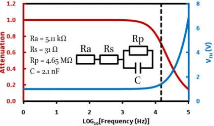
5.2 Impact of series impedance on a LC cell electro-optic response ... 71
5.2.1 Series resistance ... 71
5.2.2 Series capacitor impact ... 76
5.2.3 Simulated impact of a P3HT:PCBM layer. ... 78
5.2.4 Conclusion ...81
5.3 OASLMs lateral resolution ...81
6 OASLM with a P3HT:PCBM layer ... 88
6.1 Pure P3HT as PCL ... 89
6.2 P3HT:PCBM blends ... 94
6.3 Additional measurements ... 101
Contents
6.3.2 Electrical behaviour ... 104
6.3.3 Voc estimation from optical measurements ... 105
6.3.4 Measurement of the angle of pretilt ... 109
6.3.5 Diffraction efficiency ... 111
6.4 Conclusion ... 114
7 Impact of interfacial layers ... 115
7.1 PEDOT:PSS as an interfacial layer between the PCL and the LC. ... 115
7.2 OASLM with P3HT:PCBM used as photoconductive layer ... 117
7.2.1 Photoconductivity of P3HT:PCBM ... 118
7.3 Selection of appropriates interfaces ... 123
7.4 OASLM with P3HT:PCBM used as photovoltaic layer. ... 126
7.5 Electrical measurements ... 129
7.5.1 Current versus time measurements ... 129
7.5.2 Current vs voltage measurements ... 131
7.5.3 Impact of surface resistivity in PV OASLMs ... 135
7.6 Conclusion ... 139
8 Conclusions & perspectives ... 141
9 Résumé de la thèse en français ... 144
9.1 Introduction ... 144
9.1.1 Principe de fonctionnement ... 145
9.2 Méthodes ... 146
9.2.1 Conception des OASLMs ... 146
9.2.2 Caractérisation électro-optique des OASLMs ... 147
9.3 Résultats importants ... 148
9.3.1 OASLMs avec une couche P3HT:PCBM ... 149
Contents
9.4 Conclusion générale ... 153
9.5 Contributions scientifiques ... 156
9.5.1 Contributions par affiches ... 156
9.5.2 Brevet ... 156
9.5.3 Publication ... 156
BIBLIOGRAPHY AND APPENDIX CONTENT ... 157
Résumé ... 201
List of Abbreviations
List of Abbreviations
A Acceptor
AL Alignment layer C60 Buckminsterfullerene
CPI Cross-Polarized Intensity D Donor
DGA Direction Générale de l'Armement
DSTL Defence Science and Technology Laboratory EA Electron Affinity
HOMO Highest Occupied Molecular Orbital IP Ionisation Potential
ITO Indium Tin Oxide LC Liquid Crystal
LCD Liquid Crystal Display LCLV Liquid Crystal Light Valve
LUMO Lowest Unoccupied Molecular Orbital LV Light Valve
OASLM Optically Addressed Spatial Light Modulator OFET Organic Field-Effect Transistor
OLED Organic Light-Emitting Diode
ORFID Organic Radio-Frequency Identification Devices P3HT Poly(3-hexylthiophène-2,5-diyl)
PCBM [6,6]-Phenyl-C61-Butyric acid Methyl ester PCL Photoconductive Layer
PEDOT Poly-(3,4-ethylenedioxythiophene) PEIE Polyethylenimine-ethoxylated PSS Polystyrene Sulfonate Sodium PVK Poly-(N-vinyl carbazole)
PVL Photovoltaic Layer
SCLC Space charge limited current SLM Spatial Light Modulator WF Work Function
Introduction
1
Introduction
Who can predict the future impact of scientific discoveries in people's daily lives? Today's adds exhort us to buy the novel Organic Light-Emitting Diode (OLED) [1] television stating that "life is in every pixel". The road that led to this scientifically questionable but catchy slogan was long. It necessitated a considerable amount of efforts, time and long debates.
When Faraday discovered in 1833 [2], that, in some materials, electrical conductivity can be enhanced with increasing temperature, he did not realize that he made the first documented observation of a material class that we now call semiconductor. In addition, it was impossible for Friedrich Wöhler to anticipate the fact that when he synthesized urea in 1828 [3], organic synthesis will be another option to tailor semiconductors. At that time, scientific issues were different, but thanks to them and countless scientists, organic electronic was able to see the light of day.
Nowadays, conventional electronics mainly rely on inorganic semiconducting materials such as amorphous or crystalline silicon. Nonetheless, times are changing and silicon starts to be partially substituted by plastic electronics. It is a slow ongoing metamorphosis, only visible to the general public via commercial advertisements. Even though the main market for organic electronics is the OLED display's technology, other applications may find their way into our daily lives: OLED lightning [4], Organic Solar Cells (OSC) [5], organic field-effect transistor (OFET) [6], and Organic Radio-Frequency Identification Devices (ORFID) [7], to mention just a few.
For longer-term applications, organic materials are possible candidates as laser gain material [8], for thermoelectricity [9], or magnetoresistance applications [10]. More specifically, in our research team at ICube laboratory, organic semiconducting materials have been used for organic solar cells [11], to tailor gas sensors [11] and in 2014, via a French-UK collaboration, I started working on
Introduction
implementing these materials in Optically Addressed Spatial Light Modulators (OASLM) [12]. The latter is the main topic of my PhD project.
It is important to know that this subject gathers experts from different fields: Mathematics, optics, physics of semiconductors, organic chemistry and electronics. As a consequence, the people involved in my project work often originate from different disciplines and countries. Will I be capable to understand the very essence of what these people have to teach me? Fortunately, everyone speaks English, and therefore the language is not the main barrier. Nevertheless, I was not prepared after a master’s degree in microelectronics to deal with the fact that these people do not necessarily speak a common scientific language. It turns out that each scientific field has its own dialect, each community has its specific characteristics. For this reason, I realized that I needed to become proficient in basic communication skills with chemists, mathematician… This observation leads us to the next question.
Am I competent to work on this subject? I quickly understood that the answer is no. However, it has to be like this. At first, when I read the project, it seemed simple and I was confident. Replacing one inorganic photoconductor with its organic counterpart seemed easy. Yet, as the years went by, the well-defined outline of the project became more and more fuzzy. Who could predict with assurance the result of experiences not yet performed? This is the reason why I am writing this manuscript. A student without prior knowledge of the subject might be the more qualified for the job because he has time to learn and “try different things that have a low success rate” in other terms doing research.
During the bibliography phase inherent to every PhD student, I realized that all books or communications in my field of studies were very specific to a scientific domain. Consequently, it was difficult to understand them at first. For example, from a chemist point of view, liquid crystals are molecules with a certain chemical structure. Therefore, if chemists write a publication or a book, they will focus on the synthesis of liquid crystals. From a physical point of view, liquid crystals are rod-shaped molecules with a dipole. They consider liquid crystals as a molecule or mixture of molecules defined by physical parameters, for example, refractive
Introduction
index, elastic or dielectric constants. In order to simplify complex problems, some parameters should be set aside. The issues are also not exactly the same when it comes to the manufacturing of liquid crystal devices, which is the perspective of an engineer. With no prior knowledge of such a vast domain, a life is not long enough to become an expert. Nevertheless, one has to start somewhere and unfortunately, I did not find a book named OASδε “for beginners” when I began my thesis.
I hope that this manuscript will be more accessible to students or researchers that may have an interest for this topic and that by reading this document, they will be less lost than I was at the time. This might be the harder part to succeed and it is up to you, the reader, to decide if I have accomplished this last task.
Light valves (LV) and optically addressable spatial light modulators (OASLMs) are now part of a well-established technology. Currently available designs mainly rely on combining a photoconductive inorganic window, such as crystalline semiconductors (Gallium arsenide (GaAs) [13], Silicon (c-Si) [14]…) or amorphous silicon (a-Si) [15] with a liquid crystal layer. While reliable, their design is mainly limited to the reflection mode, as these photoconductors are strongly absorbing in the visible part of the spectrum. The spatial resolution of such devices is limited by charge diffusion in the photoconductive layer due to their inherently high charge carrier mobilities. In addition, the production costs of these technologies remain high.
For all these reasons, photosensitive organic semiconductors [16], [17] can compete with their inorganic counterparts for OASLM applications. They are not only responsive to light but are also easily processed at low cost from solution or by sublimation under vacuum and their absorption spectrum can be tuned (through molecular engineering). Additionally, the typically three orders of magnitude lower charge carrier mobility of organic semiconductors compared to amorphous silicon limits lateral charge diffusion and should lead to an improved spatial resolution.
Introduction
During my PhD project, I aimed to use a new class of organic semiconductors as the photosensitive layer in a liquid crystal OASLM, to investigate the underlying physical processes and to optimize the device performances.
The manuscript is organized as follows:
Chapter 2 repeats the general working principles of OASLMs followed by a detailed description of the different elements constituting such devices. The chapter will end with a presentation of the basic properties of organic semiconductors since these materials will be used as photosensitive layers in OASLMs.
Chapter 3 describes the different families of semiconductors used previously as photoconductive layers to tailor OASLMs. We will review the advantages and weaknesses of each technology such as inorganic crystals, inorganic thin films and organic semiconductors. In each case, we will describe the applications for which they have been designed or their potential uses.
Chapter 4 presents the organic semiconductors, P3HT and PCBM, used in my work and the OASLM fabrication procedure that I developed. The test bench that has been designed as well as the electro-optical characterization methods that I implemented, namely cross-polarized intensity (CPI), voltage transfer function (VTF), and impedance spectroscopy (IS), will be described in detail.
In Chapter 5 our first results obtained on liquid-crystal OASLMs will be described. A detailed analysis of CPI, VTF and IS data treatments will also be given. In order to better understand the impact of a change in the photoconductive layer impedance on the device response, the electro-optical response of a “standard”, i.e. non-photosensitive, LC cell will be presented. Although these tests were initiated to evaluate our device elaboration and characterization processes, the results give some useful hints for the interpretation of CPI, VTF and IS data obtained on OASLMs including an organic semiconductor layer. The last section covers the issue of OASLM spatial resolution. While our experimental set-up did not allow us to measure the resolution, I introduce a simple electrical model that allows us to clarify the link
Introduction
between the OASLM resolution and the electrical properties of the photosensitive layer.
Chapter 6 presents the behaviour of OASLMs including a blend of organic semiconducting materials (P3HT and PCBM) at different mass ratios. A detailed analysis of the experimental is given and reveals in particular that the organic layer does not behave as a standard photoconductive cell. The possible contribution of a photovoltaic effect to the device response is discussed.
Chapter 7 describes the changes brought in by modifying the nature of interfacial layers. In particular, the impact of interface engineering on photosensitivity, lateral resolution and LC alignment are discussed and used to rationalize the OASLM response. Finally, new routes to increase the performances of photovoltaic OASLMs will be presented.
Scientific Background
2
S
CIENTIFIC
B
ACKGROUND
In this chapter, we will begin by describing the working principle of optically addressed spatial light modulators (OASLMs). Afterwards, we will give more details on the different elements constituting such devices. Finally, we will discuss the reasons leading us to use organic semiconductors as photoactive materials in OASLMs.
2.1 Optically Addressed Spatial Light Modulators
A spatial light modulator (SLM) is a device that controls light in two dimensions. It consists of an address part and a light modulation part. The information written in the address part changes the optical characteristics of the light modulation part. The modulation of the readout light properties such as polarization state or intensity is tuned by the command part, producing an optical output that reflects the written information.
The simplest example of a spatial light modulator that you can find in everyday life is addressed electrically. It is used to change the amount of reflected light on a two-dimensional pixelated array. In short the screen of your calculator. There are many varieties of spatial light modulators: SLMs can be reflective, transmissive or transparent, controlled electrically or, in our case, optically.
Unlike electrically addressed spatial light modulators (EASLM) that use an addressing circuit formed on a silicon substrate with a pixel array structure [18], optically addressed spatial light modulators (OASδε’s) use a photosensitive material to control the light modulation part [19]. Transmissive OASLMs are the subject of our studies. They are also referred to as "light valve". The light modulation material can be a non-linear optical crystal such as lithium niobate (LiNbO3) [20], or more commonly a liquid crystal (LC) layer. The latter was used
in the course of this thesis due to its unique feature to control light properties as a function of molecular orientation, which can be tuned by the application of an electric field. These devices are helpful for the treatment of optical information,
Scientific Background
like real-time incoherent to coherent conversion [21], projection displays [22], optical limiters [23] and holography [24] [25].
A typical LC device can be used to change light properties such as its polarization state or transmitted intensity as a function of an applied voltage. Its device structure is as follows: A LC material is sandwiched between two transparent conductive electrodes, generally made of Indium Tin Oxide (ITO) glass plates coated with a LC alignment layer such as polyimide (PI), which will be described later. An electric potential applied to both electrodes drops across the different layers according to their electrical properties (dielectric constant, thickness, resistivity…). As an example, if the alignment layer is more resistive than the LC layer, the potential drop will be more important across the alignment layer and vice versa. The potential drop occurring across the LC layer and thus the value of the electric field controls the orientation of the LC molecules, which affects the optical properties of the LC medium.
The above description forms the fundamental basis of OASLMs made of a LC and a photoconductive layer (PCL).
If we replace one of the alignment layers with a photoresistive material assuming for simplicity that it also acts as an alignment layer, its conductivity will vary as a function of illumination intensity. Therefore, the potential drop across the LC cell and consequently the LC molecular orientation affecting the light properties will depend on light intensity as depicted in Figure 1.
Scientific Background
Figure 1: Schematic representation of a transmissive OASLM. Liquid crystal (LC) is sandwiched between two conductive glass slides (ITO), one of the ITO glass slides is coated with a thin insulating polymer layer, which serves as an alignment layer (AL), and the other ITO glass slide is coated with a photoconductive layer (PCL). Depending
on illumination intensity, charge carriers are generated, which modifies the PCL
impedance and change the voltage drop across the PCL layer (VPCL) consequently
altering the voltage drop across the LC layer (VLC).
A polarized incident light ray interacts strongly with such a device. This is due to the peculiar optical property of liquid crystalline materials known as birefringence. This physical property will be the subject of the next section.
2.2 Liquid crystals
2.2.1 Propagation of light through a birefringent medium
To change the properties of an incident light beam (phase, intensity or polarisation), materials with anisotropic optical properties are generally used. Anisotropic crystals like calcite have crystallographically distinct axes and interact with light in a manner that is dependent upon the orientation of the crystalline lattice with respect to the incident light. The refractive index of such an anisotropic crystal is dependent on the direction and polarization of light. Here we focus on uniaxial mediums that possesses two different refractive indices (no
Scientific Background
and ne respectively ordinary and extraordinary refractive index) also called
uniaxial materials. Birefringence (� ) is defined by the difference between the extraordinary and ordinary refractive indices of the material (� = − ). Figure 2 illustrates the effect of linearly polarized light travelling through a birefringent medium. In this arrangement, the transmission axis of the linearly polarized light (dashed black line) is half-way (45°) between the horizontal and vertical axis of the medium (black axis). Both, the vertical (blue line) and the horizontal (red line) components are initially in phase. When the light propagates through the birefringent medium, both components experience different refractive indices (no≠ ne) and therefore different phase velocities = and
=
� (c: Speed of light in vacuum). In this example, the refractive index of the vertical component is supposed to be higher than the horizontal one, i.e. the blue component “slows down”. Therefore, the phase difference between the two components increases as light travel through the medium. Their sum (black dashed line) or polarization is changing. In the example Figure 2, when the light ray exits the material, the originally linearly polarized light is elliptically polarized at the output.
Figure 2: Propagation of light through a birefringent medium
Polarization at the output varies as a function of light wavelength ( ), material thickness ( ), birefringence (� ) and polarization at the input.
Scientific Background
Waveplates are a common application of birefringent crystalline material and are often made of quartz. Careful adjustment of the crystal thickness is used to set the phase difference between both components of a specified wavelength to either π (half-wave plate) or π/2 (quarter-wave plate).
2.2.2 Liquid crystalline state
The first rule that we learn in school about states of matter is that three states exist: solid, liquid and gas. Nevertheless, if a rule exists, it has exceptions. In the field of matter states, one of these exceptions is the liquid crystalline state.
Although there seem to be some contradictions within the term “liquid crystal” (LC), it implies that these materials possess properties from both states. A material in the liquid crystalline phase is fluid and, when observed under polarized light, shows birefringent properties, indicating some order within the material.
In the 1880s, Friedrich Reinitzer an Austrian chemist and botanist discovered the first liquid crystal phase while working on cholesteryl benzoate. He found that this material possessed two melting points. At 145.5°C, the crystal melted into a distinctive state, which exists until 178.5°C where it became liquid. Convinced that his unusual observations were an important discovery, he collaborated with Otto Lehmann who obtained his PhD at the University of Strasbourg under the direction of crystallographer Paul Groth. Using a heating stage on a microscope with polarizing filters, he made experiments that confirmed Reinitzer's initial observations. Together they discovered this new state of matter, showing that something in-between solid and liquid exists. There are different classes of LC materials. The work of Georges Friedel established a classification scheme of the different LC phases. In this work, we will focus on thermotropic nematic (rod-like) LCs.
Nematic liquid crystals are composed of molecules that have a longitudinal, rod-like shape. This class of thermotropic LCs possess a nematic phase within a certain temperature range, as shown Figure 3. Below the melting temperature (Tm), the material crystallizes and each molecule has its specific position forming
Scientific Background
a periodic arrangement. Above the clearing temperature (Tc), the positions of the molecules are randomly distributed and the material acts as an isotropic fluid. Between these two points, the nematic phase exists. The periodic arrangement is lost and molecules orient themselves due to neighbouring molecules. An average director represents the average direction of all molecules ⃗ , but individual molecules may be more or less aligned with this vector.
Figure 3: Phase of thermotropic liquid crystalline material as a function of temperature.
In the nematic phase, the material appears milky, because many small domains exist (except if a special treatment has been applied), each with its own orientation.
2.3 Alignment layer
By depositing a layer of LCs on a glass substrate, the molecules will not be uniformly oriented along a single direction. However, most optical applications require a well-defined LC orientation. The deposition of a thin polymer film over the substrate subsequently rubbed using a rotating cloth, as depicted in Figure 4, permits the alignment of the LC molecules. The contact between the cloth and the polymer layer creates microscopic grooves on the surfaces of the polymer and
Scientific Background
aligns polymer chains [26]. Non-contact methods do also exist, such as photo-alignment, which uses polarized UV light to generate order on a photo-alignable material. In this work, we will exclusively use the rubbing method.
Figure 4: Generation of uniform alignment with the rubbing technique, a rubbing cloth is taped on a rotating drum, the polymer-coated substrate is moving toward the rotating drum. This treatment forces the organisation of the first layer of molecules.
Polyimides, whose structure is displayed in Figure 5, are an example of polymers routinely used as alignment layer material. They exhibit high thermal stability, are lightweight, cheap and easy to deposit.
Figure 5: Chemical structure of polyimide
2.3.1 Operating principle of LC devices
LCs and alignment layers introduced in the previous section are the building blocks of liquid crystal devices.
Scientific Background
The main applications of LCs are display devices (LCDs). In its simplest form, the LC material is sandwiched between two substrates with electrodes and alignment layers facing the inside of the cell. When a voltage is applied to the electrodes, an electric field is created which applies a torque to the LCs molecules so that their orientation is modified. It is important to note that the voltage applied needs to be superior to a certain threshold value called the Fréedericksz transition. Below this value, no reorientation occurs. Its value depends on the liquid crystalline material used. When LCs molecule reorients, the birefringence value changes, leading the incident polarized light to a different polarization state.
Generally, LC molecules possess an electric dipole moment. The electric dipole can be parallel to the long axis of the molecule, as shown in Figure 6, or perpendicular to the long axis of the molecule, as depicted in Figure 7. The chemical structure of the LC molecules affects the direction of the electrical dipole moment, which in turn leads to different electrical and optical properties. Above a critical voltage, the molecular dipoles reorient parallel to the electric field.
Figure 6: Nematic LC molecule with an initial planar orientation with respect to the substrate surface, a longitudinal dipole moment and positive dielectric anisotropy.
The direction and amplitude of the dipole moment of the molecule determine the dielectric anisotropy defined as ∆ = ‖− ⊥, with ‖ and ⊥ being the dielectric constants parallel and perpendicular to the average direction of the δC molecule’s long axes, respectively. LC molecules with a dipole moment directed along their long molecular axis lead to positive dielectric anisotropy (∆ = ‖− ⊥> ),
Scientific Background
whereas LC molecule with a dipole moment direction perpendicular to their long molecular axis leads to negative dielectric anisotropy (∆ = ‖− ⊥ < ).
Figure 7: Nematic LC molecule with an initial vertical orientation with respect to the substrate surface, a transversal dipole moment and negative dielectric anisotropy.
Commercially available liquid crystalline materials are rarely composed of a single molecule. Different LC molecules are blended together forming a so-called mixture. The liquid crystal optoelectronic properties, such as the Fréedericksz threshold voltage, birefringence etc. depends on the type of LC materials used and on their molar ratio.
Apart from the mixture composition, device engineering is another way to tune the response of a LC cell. The substrate properties need to be taken into account in order to align LC molecules. For instance, the alignment layer used to obtain an initially vertical orientation of 90° is different from the one used to obtain a planar orientation (0°).
It is sometimes desirable to form a small angle (also known as the pre-tilt angle) between the LC molecules and the substrate plane to reduce the threshold voltage or to increase the switching speed. The counterpart is that doing so, the LC cell birefringence diminishes because the molecules are already tilted before the application of an electric field.
An angle can also be formed between the two aligning substrates, which results in a twisted cell. The discovery of the so-called twisted-nematic effect was a
Scientific Background
breakthrough that permitted the use of LCs in displays [27] (see below). This type of cells is used to control the intensity of transmitted light. When placed between properly arranged polarizers, each polarizer is oriented with its axis parallel to the rubbing direction of the adjacent electrode (so that the polarizer and analyzer are crossed), the LC pixel appears transparent due to the induced rotation of light in the LC cell waveguide by 90°. When a voltage is applied, the LC molecules reorient, the birefringence tends toward zero and the LC cell becomes dark.
2.3.1.1 Examples of LC devices
In my thesis, I mainly used homogeneously aligned anti-parallel cells (where the top and bottom substrates are rubbed in the opposite direction, to avoid a splay deformation [28]). This corresponds to a liquid crystal device geometry that is used to change the polarization of light as a function of the applied voltage. Figure 8 depicts the two different types of LC cells and their respective response as a function of an applied bias.
Figure 8: On top homogeneously aligned anti-parallel LC cell structure (left) and light transmission as a function of the applied bias (right). Below, homogeneously aligned Twisted Nematic cell structure (left) and light transmission as a function of the applied bias (right). The arrows indicate the rubbing direction both cells are filled with a liquid
Scientific Background
The transmission versus voltage curve of a homogeneously aligned anti-parallel cell is a consequence of the LC birefringence properties that was discussed in section 2.2.1. When a monochromatic ray of light is polarized at 45° with respect to the slow and fast axis of the LC material, its output polarization at the cell exit depends on the wavelength of the light, the cell thickness and total birefringence of the LC material. In the example shown in Figure 8, the output polarization is opposite to the polarizer (analyzer) axis and the fact, that without applied bias the cell transmission is close to null, depicts this particular case. With increasing applied voltage, we observe the Fréedericksz transition (around 1V) after which the LC molecules start to reorient inducing a birefringence decrease resulting in a different polarization state at the cell output.
In the twisted nematic configuration, the directions of the LC molecular alignment on both plates exhibit an angle of 90°. This induces a continuous rotation of the long axes of the liquid crystal molecules across the LC layer thickness. The polarisation direction of linearly polarized light travelling through such a twisted-nematic configuration follows the rotation of the molecule's long axes (this is the so-called twisted-nematic effect). At the cell output, the light is rotated by 90°, following the twist formed by the LC molecules. When such a layer is placed between linear cross polarizer with its axis parallel to the rubbing direction of the adjacent electrode, the light rotates by 90° due to the LC cell and can pass the second (crossed) polarizer. Inversely, if the second polarizer direction is the same as the first polarizer, the light is blocked. In Figure 8, the polarizers are crossed and the wavelength monochromatic. With increasing voltage, the LC molecules reorient, breaking the twisted configuration so that the light polarisation does not rotate by 90° and is blocked. This principle is still used nowadays for displays based on the twisted nematic effect.
2.3.2 Liquid crystal devices driven by a DC field
Ions are always present in liquid crystals. They may result from an undesired contamination during cell manufacturing. The glue used to encapsulate the cell, as well as the spacers and alignment layers, may contain ions that can diffuse into the LC.
Scientific Background
Unwanted ionic contamination is known to have a negative impact on the LC cell performances and many studies have been made to reduce ionic contamination. For example, the use of nanoparticles that trap ions and decrease the overall ionic conductivity of liquid crystals, have been reviewed in reference [29].
One detrimental effect of ionic contamination occurs when the LC cell is driven by a DC bias. When a DC electric field is applied across a LC cell, ions start to drift towards their respective electrodes (which are supposed to be impermeable to ions): positive ions move towards the negatively charged electrode and negative ions towards the positive electrode. As a result, accumulated ions compensate the charges accumulated at the electrode and the potential gradient is limited to a region close to the electrodes. In addition, selective adsorption of ions by the alignment layer cause an irreversible performance degradation of the LC cell subjected to a DC bias [30].
Figure 9: Schematic representation of ionic charge build-up and potential vs distance as a function of time when a LC cell is driven by a DC field.
This effect is commonly referred to as electrical double layer (EDL). It cancels the effect of the voltage on the liquid crystal orientation. For this reason, LC-based devices are generally driven by AC fields.
Scientific Background
2.4 Photoconductive layer
Photoconductivity is the phenomenon that gives rise to a change in the electrical resistivity of a material upon illumination. This phenomenon is generally observed in semiconducting materials. The properties of semiconductors can be understood in terms of the band structure sketched in Figure 10. The valence and conduction energy bands indicate the possible energy states of the most weakly bonded electrons in the crystal and are separated by an energy gap or bandgap (Bg). At thermal equilibrium, the probability that an electron occupies a state of energy E is given by the Fermi-Dirac function, which depends on the Fermi level position (EF). The electrons occupying states of the conduction band (so-called
conduction electrons) and empty states of the valence band (or holes) are responsible for the electrical conductivity. It is important to note that, according to the band theory, a full energy band (for instance the valence band at ) does not contribute to an electrical current.
For a metal, the valence and conduction bands overlap (no energy gap). The resulting band is partially filled and leads therefore to a high conductivity. In an insulator, both bands are separated by a large bandgap (Bg), that renders the probability for an electron to reach the conduction band negligible. Finally, semiconductors possess a small bandgap (1-3 eV). At non-zero temperature, thermal energy allows electrons to transit from the valence band to the conduction band, leading to a non-zero temperature-dependent conductivity. These different situations are depicted in Figure 10.
Scientific Background
Figure 10: Schematic of band theory.
Light absorption is another way to excite electrons from the valence band to the conduction band, provided that the photon energy is larger than the bandgap. As depicted in Figure 11, the vacuum level is generally taken as a reference to define the conduction and valence band edges. The energy difference between the vacuum level and the Fermi level is the work function (WF). The electron affinity
(EA) is the energy gained if you add an electron from the vacuum to the bottom of the conduction band (Ec). Finally, the ionization potential (IP) is the amount of energy required to remove the most loosely bound electrons from the valence band (Ev).
Scientific Background
A photoconductor is generally composed of a slab of semiconductor (in bulk or thin film form) with ohmic contacts affixed to opposite ends. By definition, “Ohmic contacts” induce a negligible voltage drop, compared to the voltage drop across the semiconductor bulk, when current is flowing across the device. Under illumination, free charge carriers (i.e. conduction electrons and holes) are generated either by band-to-band transitions (intrinsic) or by transitions involving forbidden-gap energy levels (extrinsic). In both cases, the conductivity increases [31].
From the previous definition, we learn that two routes exist in order to generate free carriers from light absorption. The first one is to use photons whose energy is higher than the bandgap energy difference, also called intrinsic transition. In this case, the long wavelength cutoff is given by:
=ℎ =
�
where h is the Planck constant, c the light celerity and c is the wavelength
corresponding to the semiconductor bandgap Eg. For a photoconductor, the conductivity is given by:
� = + ,
where nand p are the electrons and holes mobility, n and p are the electron and
hole densities and q the elementary charge. The increase of conductivity under illumination is mainly due to the increase in the number of carriers. "Semi-insulating (SI)" or intrinsic (undoped) semiconductors with a low charge carrier density are generally used. In this case, a low light intensity is sufficient to generate more charge-carriers than the density already present in the dark state. The density of charge carriers in the dark state is therefore an important parameter that influences the sensitivity (detectivity) of the photoconductor. For sub-bandgap or extrinsic transitions, discrete energy levels within the band-gap, due for instance to defects in the crystalline lattice or impurities, must be
Scientific Background
present. In such cases, the long wavelength cutoff is determined by the defects energy level position within the bandgap.
Generally, inorganic materials (such as amorphous silicon, BaTiO3, CdTe, GaAs, InP…) are used as photoconductive layers. Unfortunately, these photosensitive materials are generally thick (hundreds of micrometres) and decrease the OASLM's transparency. Moreover, the high charge carrier mobility in some inorganic photoconductive crystals lead to lateral charge diffusion that limit the spatial resolution of OASLM devices [32]. In addition, the production costs of these materials remain high. Replacing inorganic photoconductors with novel organic photoconductors having the potential to increase the resolution and reduce the OASLM production costs is the main motivation of my PhD thesis.
2.5 Organic semiconductors
Organic materials are carbon-based molecules or polymers that can adopt a crystalline, semi-crystalline or amorphous structure. We can categorize organic materials into two families. Low molecular weight materials or small molecules and higher molecular weight polymers. This difference has its importance when it comes to implement the material in a device. Though both polymers and small molecules can be deposited in thin layers using a wet deposition method (spin-coating, doctor blading, inkjet printing …), only small molecules can be thermally evaporated.
Rather than using crystalline inorganic semiconductors, whose arrangement of atoms in crystalline lattice gives rise to delocalised electronic states and band structure, an alternative approach is to use organic semiconductors with intrinsic semiconducting behaviour. Semiconducting organic molecules include generally chains of sp2-hybridised carbon atoms. The existence of π electrons, whose
orbitals are delocalized along the molecular backbone give rise to the semiconducting properties. More or less random intramolecular coupling (between the molecular segments along the polymer chain) and/or intermolecular coupling (between the π orbitals of neighbouring molecules) give rise to a Gaussian distribution of the molecular orbital energy levels named
Scientific Background
HOMO (Highest Occupied Molecular Orbital) and LUMO (Lowest Unoccupied Molecular Orbital) levels. These energy level distributions are named HOMO and LUMO band, respectively, and play a similar role to the valence and conduction bands of inorganic semiconductors. HOMO and LUMO are often referred to as frontier orbitals, and can respectively be determined by measuring the IP and EA of the material (see Figure 11 in the previous section). The HOMO (IP) and LUMO (EA) energy difference corresponding to the electrochemical bandgap of the organic semiconductor.
The fact that organic semiconductors can be processed from solution is a major advantage compared to rigid, thick (hundreds of microns) silicon wafers with a limited surface area obtained from Czochralski processes [33] at high temperature (more than one thousand degree Celsius). Organic materials are more flexible, thinner (hundreds of nanometers) and can be processed at low temperature (from room temperature up to a few hundreds of degree). Although it is unlikely to replace silicon by organic semiconductors in high-end electronic circuitry like central processing units, in view of the ease of implementation of these materials, applications that require flexibility and/or large areas might be cheaper to produce using organic semiconductors.
Unfortunately, organic materials have several drawbacks: lower charge-carrier mobility, sensitivity to ambient atmosphere (oxygen for instance) that affect their lifespan and one major drawback for the application of this project, which requires a high photosensitivity: the strong exciton binding energy and limited diffusion length.
2.5.1 Overcoming the exciton high binding energy and small
diffusion length in organic semiconductors
Organic semiconductors (OSC) are van der Waals materials, i.e. low-density materials with weak intermolecular coupling, and are therefore characterized by a rather low relative permittivity r (typically between 3 and 4). Therefore,
absorption of photons with energies above the OSC band-gap generates coulombically bound electron-hole pairs (or “excitons”) rather than free charge carriers.
Scientific Background
Dissociation of photo-induced excitons into free charge carriers may be achieved by introducing a heterojunction composed of an electron-donor (D) material (i.e. having a low ionisation potential) and an electron-acceptor (A) material (i.e. having a high electron affinity). If the differences in electron affinity and ionisation potential between both materials are sufficiently large (typically above 0.3 eV which correspond roughly to the exciton binding energy [34]), excitons generated close enough to the D/A interface may be dissociated into a pair of free charge carriers by charge transfer (CT) from the D to the A (or vice versa). An illustration of this concept is depicted in Figure 12. Note that to make this mechanism efficient, most photons need to be absorbed at a distance less than the exciton diffusion length to the D/A interface (i.e. typically less than 10 nanometers [35]).
To overcome this bottleneck, the concept of bulk heterojunction (BHJ) has been introduced a few decades ago [36] and has since allowed the development of organic photovoltaic devices with power conversion efficiencies exceeding 10%. In brief, in a BHJ the photon-absorbing layer is composed of a blend of D and A materials (Figure 12c) rather than of a planar D/A heterojunction (Figure 12b). Controlled micro-phase separation occurring during the film deposition or upon thermal annealing leads to an interpenetrated network of nanometre-sized D and A domains, with a large D/A interfacial area, making exciton dissociation highly efficient. The free charge carrier density (and therefore the electrical conductivity) in a BHJ increases upon exposure to light.
Scientific Background
Figure 12: Energy level diagram of an organic heterojunction (a) and schematic representation of a planar (b) and bulk (c) heterojunction.
If similar electrodes are used on both sides of the heterojunction and if the random morphology is isotropic, a metal/BHJ/Metal device will act as a photoresistor. In other words, if no external voltage is applied, the free carriers will have no preferential pathway towards the electrodes. Therefore, no current should flow and no voltage difference should appear at the device electrodes under illumination.
2.6 Thesis in context
My thesis is in the continuity of the work done by the Soft Photonic Systems Group led by Professor Malgosia Kaczmarek from Southampton University. They have been working on OASLMs using PVK (Poly-(N-vinyl carbazole)) a polymer historically used as xerographic photoreceptors since 1970 [37].
PVK is an electron-donating molecule when blended with electron-accepting molecules such as fullerene (C60) or trinitrofluorenone (TNF). It shows
interesting photoconductive properties [37]. Due to its wide band-gap (3.5 eV) PVK possess the advantage of being almost transparent to visible light. Unfortunately, this system, although functional, suffers from several drawbacks.
Scientific Background
Its operation in an OASLM has been found to be limited to low frequencies (< 1 Hz) [38]. Also if the conductivity (due to ionic impurity) of the LC mixture is too high, no liquid crystal modulation by light can be achieved [38]. To address these issues, novel organic materials circumventing those drawbacks are needed.
To address the need for novel organic semiconductors, a collaboration was initiated between the groups of Malgosia Kaczmarek, specialized in the experimental and theoretical response of light modulators from Southampton University, and the group of Thomas Heiser specialized in devices made of organic semiconducting materials, from Strasbourg University. A UK-French PhD program, jointly managed by DGA and DSTL, funded this work.
State of the art
3
State of the art
The numbers of photoconductors and LCs available on the market are high, so is the number of possible combinations of both objects to design an OASLM. In this section, we will focus on state of the art photoconductors. We can classify them into three categories: Bulk inorganic crystals, inorganic thin films and organic thin films. Several parameters are important such as the spectral sensitivity, the transparency/reflectivity, the spatial resolution, the working frequency, the response time and the fabrication method, which influences the device cost.
The required specifications depend on the focused application. As an example, for the design of a light valve that acts as an optical shutter to protect for instance human eyes from high light intensity, it is most necessary to use transparent photoconductors with a sufficiently high response time, whereas the spatial resolution is not very important. However, if the goal is to design an OASLM for telecom applications that widely use wavelengths around 1500 nm, the transparency in the visible is not as important as the transparency and photosensitivity in the Infrared (IR) region. If the objective is to encrypt an image as a function of LC modulation in holographic applications, the spatial resolution is most important. For a display device, the resolution is limited by the pixel size and is defined by the following equation:
. − = /
× �
The perfect photoconductor does not exist. There are pros and cons for each semiconductor technology, as illustrated in this chapter.
3.1 Bulk Semiconductor Crystals
Modern semiconducting technologies mainly rely on monocrystalline substrates made of Silicon or III-V compounds. The common trait of these semiconductors is that they have been manufactured using a crystal growth method, the
State of the art
Czochralski process [33] being the most frequently used technique. The thickness of such commercial wafers is around hundreds of micrometres and the wafer size limits the maximum device area. To my knowledge, the main advantage of this class of materials is the perfect control of most electrical and optical parameters achieved after decades of research, which facilitates the conception of an OASLM. Even the defects within the bandgap are well defined. These defects are important to define the spectral sensitivity of crystalline photoconductors, as they permit sub-bandgap absorptions. One of the best known crystalline defects used in OASLMs is the native defect level known as EL2 in Gallium arsenide (GaAs) [39] [40]. It permits to design infrared sensitive OASLMs.
3.1.1 Semi-Insulating GaAs (SI GaAs)
In the specific application of fiber optics sensors, the attenuation of the optical signal is lowest around 1500 nm. Therefore, it is necessary to choose a photoconductor sensitive to telecom wavelengths. IR sensitive GaAs photoconductors have been recently used to design an OASLM which serves as holographic medium in an adaptive interferometer based on two-beam coupling [13], [24] and is to be used in conjunction with optical fiber technology. The working principle is as follows: a linearly polarized continuous-wave fiber laser beam ( = 1.55 μm) is divided into two optical paths, forming the reference and signal wave of the interferometer. The two waves recombine on the OASLM. Along the "signal arm", a calibrated phase modulator induces a small phase shift that induces a phase grating inside the OASLM, which in turn diffracts incident light. By measuring the intensity of the diffracted orders with a photodiode, it is possible to measure small phase shift differences between the reference and the signal fiber. For some applications, the phase difference may be induced by the modulation of the signal fiber length. It can for instance, be applied to probe mechanical deformations induced by sound waves or by mechanical stress. Figure 13 schematizes the adaptive interferometer in which the OASLM is the recombining medium.
State of the art
Figure 13: (a) Adaptive interferometer setup: a 1.55 m laser source is split into two paths, reference and signal, and then recombined on the OASLM. A calibrated phase modulator is inserted in the signal arm. BS, beam splitter; D, diaphragm; L, far-field
lens (400 mm focal length); PC, polarization controller; TIA, transimpedance amplifier. (b) Two-beam coupling process occurring in the OASLM. Reproduced from
[13]
Even though the light modulation has been demonstrated at a wavelength of 1.55 μm, the very high charge carrier mobility of this semiconductor, around 5000 cm2/(V.s), limits the spatial resolution to hundreds of microns (around 5 lp.mm-1)
due to lateral charge diffusion [32]. Improving the spatial resolution would permit the integration of OASLM in systems that are more compact. However, for non-holographic applications, the spatial resolution is less important. Moreover, it is often more interesting to use visibly transparent semiconductors (i.e. with a wide band-gap) such as silicon carbide (SiC).
3.1.2 Silicon carbide (SiC)
Silicon carbide is well-known for its polymorphism [41], which is the ability of a crystalline material to exist in more than one crystal structure. It is a complex material, due to the wide variety of polytypes, which give rise to different bandgap energies [42]. SiC bandgap varies in a broad energy range, from 2.4 to 3.3 eV. It is correlated to the material crystalline lattice structure, as illustrated Figure 14.
State of the art
Figure 14: The bandgap energies of seven SiC polytypes, namely 3C (Cubic 2.390 eV), 8H (2.80 eV), 21R (2.86 eV), 15R (2.986 eV), 33R (3.01 eV), 6H (3.023 eV) and 4H (3.263 eV), as a function of the hexagonality, reproduced from [42]. The indicated line
was only drawn as a guide to the eye.
Vanadium is known to create both a deep donor level and a deep acceptor level in 4H [43] and 6H [44] [45] SiC crystals, with the deep donor level located below the deep acceptor. It has therefore the unique capability to compensate residual dopants in order to confer semi-insulating properties to both p-type and n-type SiC, whatever polytype 4H or 6H. The position of the acceptor and donor levels for these two polytypes as a function of different crystal growth techniques has been the subject of many scientific papers and is summarized in reference [46]. 4H or 6H SiC polytypes wide band-gap photoconductors are transparent in the visible spectrum, while the presence of Vanadium related deep levels enhances its spectral sensitivity in the visible and IR range [47], [48]. The charge carrier concentration is generally very low at room temperature [44], [45] which makes V-doped SiC an ideal candidate for applications as optical limiters. The V-SiC photoconductor has been used to design a liquid crystal light valve in order to protect devices or human eyes from high-intensity light source [23] [49]. Figure
State of the art
15 depicts the operation of such devices with the LC being in a twisted nematic configuration.
Figure 15: Operation of a transparent optically addressed light valve. The cell is in the twisted nematic configuration, located in-between a polarized light source and a polarizer, an external electric field is applied to the ITO/glass sheet. When the red laser
is on, the impedance locally diminishes and the LC reorient rendering the illuminated area opaque (right). The video is available online on Ploughshare Innovations YouTube
channel. Ploughshare Innovations is the UK government’s technology transfer organisation.
3.1.3 Photorefractive crystals
Another photoconductor known as Bismuth Silicon Oxide (BSO) has particularly interesting optical properties (see reference [23]). It has been shown to be optically active, causing a wavelength-dependent rotation of linearly polarized light passing through the crystal medium. BSO belongs to the class of photorefractive semiconducting crystals. Upon illumination, the local refractive index of a photorefractive medium is modified. Consequently, the light ray self-modifies its propagation conditions in the medium. Photorefractive crystals, when used in conjunction with liquid crystals, can lead to novel properties. Lithium Niobate (LiNbO3) is another photorefractive material used as light
modulation medium in Microchannel Spatial Light Modulator (MSLM) [20].
3.1.4 Lithium niobate (LiNbO
3), a “photovoltaic substrate”
LiNbO3 has been recently used as "photovoltaic substrates" for liquid crystal cells
[50] [51]. LiNbO3 is a trigonal crystal system, which lacks inversion symmetry
State of the art
abnormal “bulk photovoltaic effect” [52]. In non-centrosymmetric crystals, such as LiNbO3, the probabilities for electron photo-excitation, electron scattering or
relaxation are anisotropic. Consequently, a photocurrent may arise under illumination and build up space charge. Such photocurrents are sometimes called “photogalvanic” currents to differentiate them from the usual photovoltaic effect. In addition, the electric field changes the refractive index of photorefractive LiNbO3.
In iron doped LiNbO3 (LiNbO3:Fe) the bulk photovoltaic effect is significantly
enhanced due to the presence of two valence states of the iron dopant: Fe2+
(donor ions) and Fe3+ (acceptor ions) [53]. Upon illumination, the excited charges
follow a statistically favourable direction of motion. Therefore, the orientation is critical to obtain an electric field in the desired direction. LiNbO3 substrates are
cut in the Z direction (C-plane). Upon illumination, it gives rise to an electric field that is perpendicular to the substrate plane as depicted Figure 16.
Figure 16: Light-induced charge separation in z-cut LiNbO3 crystals, reproduced from
[54]
A hybridized LC cell arrangement utilizing the bulk photovoltaic field and consisting of a LC layer comprised between two LiNbO3:Fe substrates was
initially proposed by Carns in 2006 [50]. When illuminated, the bulk photovoltaic effect in each substrate creates an internal electric field between the two substrates that is sufficient to reorient the LC molecules. No external electrical field is required, as illustrated in Figure 17.
State of the art
Figure 17: Principle of a voltage free LC light valve using two LiNbO3:Fe substrates cut
in the C-plane, reproduced from [50]
Such devices display a transient response of several seconds, which depends on the illumination time. The possibility to optically generate a static electric field, avoids the need for electrical contacts, wires and power generators, rendering the device more compact. Therefore, LiNbO3 is a promising material for all-optical
devices and has been suggested to be integrated in optofluidic systems, where a high degree of compactness is required [55]. However, the concept still needs to be demonstrated in practical applications.
To conclude, bulk semiconductor technology is a vast topic that has been for decades the focus of intense research, triggering its application to OASLM devices. However, they generally suffer from low resolution (some tenth of lp.mm-1) and high production costs (due for instance to high-temperature
processing). In addition, the crystal size is hard to control and impedes the development of large area devices.
3.2 Inorganic thin films
Unlike the previous bulk crystalline materials, inorganic thin films do often lack long-range structural order. Wide varieties of deposition methods are available to deposit inorganic thin films: from the utilization of a gaseous precursor to wet deposition techniques. The material process parameters strongly affect the resulting semiconducting properties and often lead to lower electronic performances. However, these materials can be processed at a lower temperature,
State of the art
allowing deposition on plastic substrates and making them compatible with roll-to-roll processing techniques. The latter has a great impact on the production costs. Inorganic semiconducting nanoparticles, such as ZnO, can be processed from solution, while amorphous silicon (a-Si) can be deposited over large areas by Plasma-Enhanced Chemical Vapor Deposition (PECVD).
3.2.1 Amorphous hydrogenated silicon
Hydrogenated amorphous silicon, a-Si:H was first fabricated by Chittick using a silane gas (SiH4) precursor [56], a hazardous gas that has already caused
explosions in photovoltaic fabrication plants [57].
Despite these technical issues, amorphous silicon possesses a major advantage compared to crystalline silicon as the photoconductive material for OASLM. The charge carrier mobility is three orders of magnitude lower [58] than its crystalline counterpart, improving the OASLM spatial resolution [32]. However, despite thinner films, the strong extinction coefficients of a-Si:H (direct bandgap material) [59] limits its use to reflexion mode structures. OASLMs based on a-Si:H thin films were first proposed by Ashley and Davis in 1987 [60]. To address the OASLM they use the reflection mode proposed by Grinberg in 1975 [61] schematize in Figure 18. In this configuration, a write light is used to address the photoconductor, which spatially modulates the LC layer. The LC spatial modulation is probed by the read-light (labelled as projection light in Figure 18) which is spatially modulated by the light pattern induced by the writing light. The dielectric mirror and the blocking layer separate the photoconductor from the read-out light.
![Figure 14: The bandgap energies of seven SiC polytypes, namely 3C (Cubic 2.390 eV), 8H (2.80 eV), 21R (2.86 eV), 15R (2.986 eV), 33R (3.01 eV), 6H (3.023 eV) and 4H (3.263 eV), as a function of the hexagonality, reproduced from [42]](https://thumb-eu.123doks.com/thumbv2/123doknet/14448638.518217/41.892.228.629.131.536/figure-bandgap-energies-polytypes-cubic-function-hexagonality-reproduced.webp)
![Figure 18:Schematic of the reflective LC light valve reproduced from [61]](https://thumb-eu.123doks.com/thumbv2/123doknet/14448638.518217/46.892.208.706.137.502/figure-schematic-reflective-lc-light-valve-reproduced.webp)
![Figure 19: Variation of hole and electron drift mobility with TNF:PVK molar ratio, reproduced from [77] at an electric field of × /](https://thumb-eu.123doks.com/thumbv2/123doknet/14448638.518217/49.892.272.595.134.549/figure-variation-electron-drift-mobility-molar-reproduced-electric.webp)