Thin Films by a Laser-Induced Thermal Gradient
The MIT Faculty has made this article openly available. Please share how this access benefits you. Your story matters.Citation Singer, Jonathan P., Pao-Tai Lin, Steven E. Kooi, Lionel C. Kimerling,
Jurgen Michel, and Edwin L. Thomas. “Direct-Write Thermocapillary Dewetting of Polymer Thin Films by a Laser-Induced Thermal
Gradient.” Advanced Materials 25, no. 42 (August 21, 2013): 6100– 6105.
As Published http://dx.doi.org/10.1002/adma.201302777
Publisher Wiley Blackwell
Version Author's final manuscript
Citable link http://hdl.handle.net/1721.1/89412
Terms of Use Article is made available in accordance with the publisher's
policy and may be subject to US copyright law. Please refer to the publisher's site for terms of use.
DOI: 10.1002/adma.((please add manuscript number))
Direct Write Thermocapillary Dewetting of Polymer Thin Films by a Laser-Induced Thermal Gradient
By Jonathan P. Singer†, Pao-Tai Lin†, Steven E. Kooi, Lionel C. Kimerling, Jurgen Michel, and Edwin L. Thomas*
[*] Prof. Edwin Thomas
Department of Mechanical Engineering and Materials Science Rice University
6100 Main Street Houston, TX 77005 E-mail: elt@rice.edu
Dr. Jonathan P Singer, Dr. Steven E. Kooi
Department of Materials Science and Engineering, Institute for Soldier Nanotechnologies Massachusetts Institute of Technology
77 Massachusetts Ave Cambridge, MA 02139
Dr. Pao-Tai Lin, Prof. Lionel C. Kimerling
Department of Materials Science and Engineering, Materials Processing Center Massachusetts Institute of Technology
77 Massachusetts Ave Cambridge, MA 02139 Dr. Jurgen Michel
Materials Processing Center
Massachusetts Institute of Technology 77 Massachusetts Ave
Cambridge, MA 02139
[†] These authors contributed equally to this work
Keywords: Direct write, Thermocapillary effect, Dewetting, Pattern transfer
The demand for lithographic methods that provide rapid, high resolution patterning with a maximum degree of control continues apace. Laser direct write (DW) is an
attractive alternative to the more ubiquitious, slower vacuum chamber particle beam DW techniques, as it can achieve up to cm/s patterning rates. These laser techniques, however, come at the cost of reduced resolution and require high numerical aperture (NA)
immersion objectives (and even the overlapping of multiple beams)[1] to achieve their most impressive sub-wavelength results. In addition, the materials employed for both laser and charged particle DW are often themselves expensive, designer materials. While
nanomachining by femtosecond ablation can also achieve sub-micron patterning in a general set of materials,[2] it often results in rough features due to the high-energy nature of the ablation process. By taking advantage of the interaction between optical and thermal effects, we have developed a positive-tone DW technique that can achieve sub-wavelength pattering by non-linear overlap effects in a conventional polymer system with relatively inexpensive free-space optics, where the resulting features are robust enough for transfer to the underlying substrate. Further, this method skips the usual development step and promises the possibility of a solvent-free lithographic technique.
We recently introduced focused laser spike (FLaSk) annealing (Figure 1a) as a DW analog to laser spike annealing (LSA). LSA, where annealing is performed by rapidly scanning a high intensity continuous or pulsed laser across an absorbing substrate, has been utilized as an alternative to a standard thermal treatment in semiconductor
technology[3] and also for the annealing of soft materials, such as the post-exposure bake of chemically amplified photoresists[4] and for inducing the microphase separation of a polystyrene-polymethylmethacrylate block copolymer.[5] In this technique, the
temperature and annealing time can be controlled by selection of laser intensity and exposure time to perform the anneal while avoiding unwanted effects, such as material degradation or component lateral diffusion. FLaSk utilizes continuous visible or near-IR light and a high numerical aperture objective to accomplish LSA on a micron or
submicron scale and has been similarly demonstrated for full 3D post-exposure bake of absorbing-dye-doped chemically amplified resists[6] and the 2D ordering and alignment of a polystyrene-polydimethylsiloxane block copolymer film swollen with ~40 vol% toluene
solvent from surrounding vapor.[7] In this latter study, the ordering mechanism was based on large thermal gradients (1-1000 K/µm) that occurred from substrate absorption to drive a type of cold zone annealing. Here, we perform DW FLaSk dewetting of a polystyrene (PS) homopolymer thin film by using the same gradients to drive thermocapillary-induced dewetting.
Dewetting has been utilized as a method to generate nanopatterns in thin films of metals[8] and polymers[9] through film-stability-based self-assembly, most generally under near-global heat provided by a hotplate or large-area pulsed LSA. In these techniques, the driving force is the large change in film surface energy due to increased temperature leading to formation and growth of isolated droplet features. A related technique based on the flow of liquids down a thermal gradient (the thermocapillary effect)[10] has been developed to form large area nanopillar arrays[11] and, most recently, for the nanoscale removal of a protective thin film by resistive heating of carbon nanotubes.[12] The generalized expression for thermocapillary force is:
T dT d n ~ ˆ (1)
Where ~ is the shear stress, nˆ the surface normal, and γ the surface tension. The surface tension almost always decreases with temperature leading to a net force down the thermal gradient. In the case of the nanopillars, the thermal gradient was generated along the film normal by using a heated substrate under a thin film, an air gap, and a floated cooled superstrate to create sharp (~50 K µm-1) thermal gradients, which drives formation of the pillars. The nanotube patterning employed similar magnitude gradients to displace a protective thin film above only the higher-resistivity, conducting tubes, with the gradients emanating from the nanotubes being essentially 1D. For the FLaSk technique, the in-plane gradients generated radially from the spot can be equal to or much greater than those
generated in either previous technique. Beyond this, FLaSk provides these gradients on-demand to a sub-micron region of the film, thus enabling a DW technique.
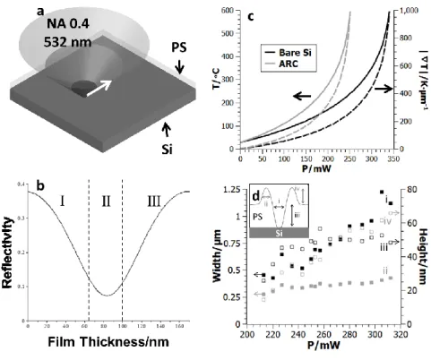
To understand the mechanism of 2D FLaSk dewetting, it is important to first consider the temperature of the silicon substrate during writing. Determining this is complicated by the fact that the polymer layer acts as an anti-reflective coating (ARC) for the silicon. The transfer matrix method (described in the SI)[13] was used to determine the expected ARC effect for the simplest case of purely normal incidence, which should apply at the laser focal point (Figure 1b). In a dewetting process, both thinning and thickening occur, since the formed trench generates a surrounding ridge by material displacement. Considering only one cycle of the periodic film-thickness ARC effect, it is possible to identify three regimes of dewetting behavior (indicated in Figure 1b): (I) where thinning the film increases reflectivity and thickening decreases it, (II) where any sizable change in thickness will result in an increase in reflectivity, and (III) where thinning the film
decreases reflectivity and thickening the film increases it. Each of these regimes can be expected to have very different pattern formation behaviors. For example, in (III) the temperature initially increases as the material thins, raising the risk of crossing the damage threshold, but then cools, making it unlikely that full dewetting will occur. (II) can be considered the “safest” thickness since any large changes in thickness result in cooling. (I) results in cooling in the highest intensity, heated, regions, and additional heating in the ridge areas and was thought to be the best initial target for high resolution patterning for reasons explained below, though all regimes will be explored in the future.
With this as a starting point, finite element method (FEM) simulations, informed by the observed damage threshold of the bare wafer, were used to estimate the
temperatures and gradients that the polymer would experience during the FLaSk anneal both with and without a 60 nm ARC (simulation details in the SI) using
temperature-dependent values for silicon thermal conductivity, heat capacity, and density,[14] along with the optical absorption of near-intrinsic silicon excited with 532 nm light.[15] Using these simulations, it is possible to plot the range of peak temperatures and thermal
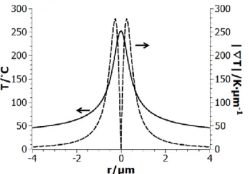
gradients in the thermal spot expected for a given power as the PS film dewets (Figure 1c). A typical thermal profile is shown in Figure S1, consisting of a FWHM=~1 µm Gaussian distribution, which for the 100 µm s-1 speed employed in this study translates roughly to a 10 ms thermal spike. During this excursion, the optical absorption can be expected to track through a range of temperatures as the film heats from the moving source and
simultaneously dewets and then cools. This is a highly complex process since the film will heat faster when it is thicker and thus likely thins before the peak temperature is reached; however, the largest magnitude thermal gradients, which are spatially in front of the temperature peak, may be experienced during this process. As a result, the full kinetics will have to remain for future work, but could be approached by an elaboration of the 1D method developed by others.[12] Regardless, it can be seen that for the power range employed (200-320 mW) gradients of approximately 100~1000 K/µm, around an order greater than those from vertical dewetting, can be expected.
The results of this dewetting can be observed by AFM, as shown in Figure 1d for isolated FLaSk lines patterned at different powers at a write speed of 100 µm s-1. Each line shows two distinct features, a trench formed by dewetting and the accompanying ridge due to the displacement of material from the trench. As can be seen, with increasing power the trench width (measured as the FWHM of the bottom of the trench to the top of the ridge) increases roughly linearly from ~0.4 to ~1.2 µm, while the depth (defined from the film surface) increases rapidly until it asymptotes at the full thickness (here ~50 nm at ~230 mW). Ridge height grows linearly, even past the asymptotic limit of the trench depth, due to the fact that the ridge width (defined as the FWHM from the surface of the film)
remains relatively stable compared to the trench width, only increasing from ~0.3 to ~0. 45 µm. This difference in feature size may be explained due to the fact that, while the trench includes increasingly more material that is above the flow temperature of the PS, the ridge is always in a low mobility region of the film, leading to a buildup. One significant feature of both the lines and ridges is that they are below both the width of the optical spot
(FWHM for ideal NA=0.4 focus is 0.66 µm) and the thermal spot size. By the metric of either feature, the apparently-linear feature increase of the single FLaSk lines still manages to possess regions of sub-optical limit resolution.
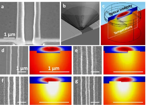
The ultimate goal for most lithographic processes is pattern transfer into the underlying substrate. Therefore, pattern transfer into silicon and FIB cross-sectioning was approached to demonstrate the capabilities for the technique (Figure 2a). It can be seen that at this power and focus the individual lines consist of ~0.85 µm width trenches
bounded by ~0.5 µm rectangular buildups, with trench depth of ~0.78 µm. The accessible depth of patterning can be increased with the selectivity of the utilized polymer, but indicates that submicron pattern transfer is even possible with a conventional polymer (like PS).
An interesting distinction between dewetting and ablation is the displacement of material as opposed to its complete removal as would be the case with ablation. Due to this, the patterning behavior of lines as the line-to-line distance decreases is of
considerable interest. An analogous phenomenon has been recently used to increase the feature resolution and pitch of nanotip indentation fabricated gratings by exploiting the overlap of the material displaced by formation of a trench.[16] While there are highly dynamic processes involved in material’s displacement by FLaSk, further FEM simulation (Figure 2 b,c) can elucidate some of these behaviors. To accomplish this, full 3D
using the observed cross-section ratios from Figure 1d as a starting point (details in the SI). The critical factor is the effect of film thickness on the optical absorption of the substrate. As shown in Figure 1b, for regime (I) lines, thicker portions of the PS film lead to higher optical absorption, while thinner films lead to lower optical absorption. The net result is that a line patterned with a majority of the focal intensity within a trench will have a lower peak temperature. Alternatively, when some portion of the incident intensity is within the ridge, a hotspot can develop with a size independent from the actual beam spot, but rather depending on the overlap. Based on this, several distinct regimes of behavior can occur. This can be seen clearly in the second line patterned, which is shown for several values of the offset between the first and second line in Figure 2d-g. As the beam spot approaches the ridge, at first (offsets between 0-0.1 µm) the temperature is insufficient to generate any line formation. Then, (at offsets of 0.2-0.4 µm) a reduced spot due to overlap and ARC effect causes the formation of very high resolution lines. Once the overlap becomes great enough (0.5-0.7 µm), the spot fills the ridge leading to larger lines and complete dewetting of the ridge (allowing for some of the uniform periodicities observed at these spacings). Finally (>0.5 µm), the line reaches the other side of the ridge and causes the formation of an entirely new line. The formation of these second lines does not necessarily leave the same spacing between the patterned region and the ridge as the line that formed it, leading to the potential for each of the successive lines to display a differing behavior. This is shown for increasing numbers of lines patterned at different spacings in Figure S2.
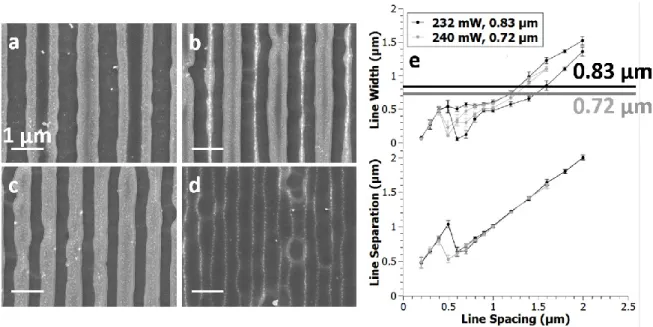
Having now developed some intuition for the patterning mechanisms, it is useful to approach a systematic set of patterns. Figure 3a-d shows several characteristic 1D grating patterns. As the periodicity changes, several regimes of patterning occur. This is shown for two sets of gratings starting from different-sized single line patterns (~0.83 µm in the
black trace corresponding to the shown SEMs in Figure 3a-d and ~0.72 µm for the grey trace). First, (not shown) the ridge spacing will be equal to the separation minus the line width when the lines are far enough away not to interact. Then (~2 µm), a bifurcated line width regime (shown for 1.4 µm in Figure 3a) will begin with alternating large and small ridges as discussed above and spacings equal to exactly the write spacing, since every line written is a line patterned. Once the widths of these features approach the isolated feature size, their width difference can be seen to narrow, as each patterned line finds itself in a very similar environment as the one prior due to the filling of the ridge observed in Figure 2. With decreasing separation, the bifurcation increases (and some spacing bifurcation is also observed) due to the overlap effect shown in Figure 2d-g until high resolution (down to ~70 nm) features are observed for the smaller line (Figure 3b for 0.7 µm, possessing ~0.1 µm features). Finally, the smaller feature disappears entirely (~0.5 µm writing
spacing), thus leading to an increase in the feature-to-feature distance. After this transition, multiple lines will pattern a single feature in a relatively uniform fashion (Figure 3c for 0.4 µm), but this behavior will only be stable down to a certain point, shown with ~70 nm features for 0.2 µm writing spacing in Figure 3d.
A few interesting observations: first, it can be noted that more than two line spacings are never (or rarely, considering all samples fabricated) observed, at least at a noticeable enough difference to exceed the displayed error bars. Rather, there seem to always be either alternating line sizes (and spacings) or a single dominate size and spacing. Why this is the case is not entirely clear, but it is definitely convenient for the purposes of a lithographic technique. One unfortunate result for the small spacings is a side effect of multiple lines patterning the same feature, which is sensitive to process fluctuations. This is especially evidenced in Figure 3c,d. The result is line ‘wiggling’ and small laser
variations or impurities. This will have to be addressed to be able to get these high resolution features with acceptable quality. That being said, the grating structures
fabricated at higher spacings are still below the optical limit (~1 µm for these optics) and are of a reasonable quality. In comparing the grey and black traces in Figure 3e, it can be seen that the transition to single, low-periodicity lines occurs later in the smaller feature patterns (grey) as may be expected, but despite this, the trend for both the feature size and spacing appears to follow the same linear traces. The slopes of these lines are ~1.7 for the line spacing and ~2.0 for the line width. Both observations are unexpected considering that, as can be seen in Figure S1, lines may be formed from different numbers of
exposures. This is a behavior that could be expected to greatly depend on the size of the optical spot. Rather, the suggestion of these observations is that there is a fundamental shape and size that is adopted for a given film thickness, polymer, and written line-to-line spacing. The last parameter, being a property of the experiment, is very surprising, and will definitely need to be investigated further both through 3D simulations of the line evolutions and experiments with different spot sizes to see if this trend holds for larger variations.
Thermocapillary dewetting of a simple polymer system (PS) was demonstrated as a positive tone direct write process that can be used effectively for pattern transfer of
submicron lines without the necessity of a development step. While this is already a useful technique, the patterning capability becomes even greater as the lines are brought together – due to the fact that the driving force for dewetting and pattern formation (proportional to thermal gradients) is a result of a combination of the optical exposure and the thermal properties of (primarily) the absorptive substrate, consecutively patterned lines near to one another possess anti-reflection effects leading to subwavelength thermal profiles. In this manner of decoupling the optical resolution from the resultant thermal pattern, isolated
features down to <100 nm or grating patterns with near constant periodicity near the optical limit (0.5-1 µm) and line widths still below the optical limit either in a large-small alternating pair or constant size may be generated. The resultant polymer film height variation features are still robust enough for pattern transfer to the underlying substrate and therefore represent a new method to create high resolution features in a three step (resist deposition, laser patterning, and etching) process, eliminating the necessity for wet chemical development. To improve the resolution and consistency of this method, the current NA (0.4) could be increased. In addition, different thin film materials possessing either more beneficial properties for patterning or pattern transfer could be approached. In the former regard, it is not clear a priori what properties will lead to superior response, but it is likely that increasing the softening temperature and decreasing the mobility (such as with higher Tg or molecular weight polymers) could achieve a smaller extent of isolated dewetted features. Finally, it may be possible to employ water or alcohol soluble polymers to completely remove the need for hazardous chemicals from the lithographic process. Experimental:
Thin Film Preparation:
Lightly doped p-type silicon substrates ([100] orientation, 10 Ω·cm) were coated with films of PS (18 kg/mol, Sigma Aldrich) from 1.8 wt% solutions in propylene glycol monomethyl ether acetate to prepare films of 50-60 nm thickness by spin coating. The film thickness was determined by ellipsometry with a J. A. Woollam Co. M-2000D spectroscopic ellipsometer.
FLaSk Annealing:
FLaSk zone annealing was performed using circularly polarized 532 nm light from a Coherent Verdi V5 diode pumped solid state laser system. Power was controlled by the system controller and measured with a power meter (Newport 818-UV) using an in-path
partially reflecting mirror placed before the lens. The power meter was also positioned after the objective to determine the amount of light that reached the sample relative to the standard positioning of the meter. The objective lens used was a Zeiss LD Achroplan 20X objective with numerical aperture 0.4. The last optic before the objective was a green dielectric mirror, allowing for simultaneous imaging in transmission with red and near-IR light from a white light source via a camera mounted above the stage. Motion of the sample for direct write was controlled by a Physik Instruments PIMars™ piezostage with 300 μm of travel on all three axes mounted on a PI M-686 stage for larger motion.
Patterning was controlled by a LabView program that controlled both the stage and an electronic shutter.
Imaging:
AFM imaging was performed with a Veeco Dimension 3100. Patterns were
transferred from polymer into the underlying Si substrate using STS ICP-RIE. The etching gas is a mixture of C4F8/SF6 with a 2 min etching time at a power of 1200 W and gas rates of 50 and 80 sccm respectively. SEM imaging was performed on a JEOL 6700 microscope at 5 keV with 8 mm working distance for top views and 15 mm working distance for the 25º angled view shown in Figure 2a after focused ion beam milling with a JEOL 9320 FIB.
Simulations:
FEM simulations of the FLaSk process were conducted using the commercial package, COMSOL Multiphysics. COMSOL allows for simultaneous solution of multiple differential equations in the same model. For this study, we used the packages for thermal conduction and electromagnetic waves.
This research was supported (in part) by the U.S. Army Research Office under contract W911NF-07-D-0004, by the Semiconductor Research Corporation, TEL and TSMC. Supporting Information is available online from Wiley InterScience or from the author.
Received: ((will be filled in by the editorial staff)) Revised: ((will be filled in by the editorial staff)) Published online: ((will be filled in by the editorial staff))
[1] a) J. Fischer, G. von Freymann, M. Wegener, Adv. Mater. 2010, 22, 3578; b) L. Li, R. R. Gattass, E. Gershgoren, H. Hwang, J. T. Fourkas, Science 2009, 324, 910; c) J. Fischer, M. Wegener, Opt. Mater. Express 2011, 1, 614.
[2] a) B. Yalizay, T. Ersoy, B. Soylu, S. Akturk, Appl. Phys. Lett. 2012, 100, 031104; b) R. R. Gattass, E. Mazur, Nat Photon 2008, 2, 219; c) M. Huang, F. Zhao, Y. Cheng, N. Xu, Z. Xu, Opt. Express 2008, 16, 19354.
[3] a) A. Gat, L. Gerzberg, J. F. Gibbons, T. J. Magee, J. Peng, J. D. Hong, Appl. Phys. Lett. 1978, 33, 775; b) Y. F. Chong, H. J. L. Gossmann, K. L. Pey, M. O. Thompson, A. T. S. Wee, C. H. Tung, IEEE T. Electron Dev. 2004, 51, 669; c) A. Shima, A. Hiraiwa, Jpn. J. Appl. Phys. 2006, 45, 5708.
[4] a) B. Jung, J. Sha, F. Paredes, C. K. Ober, M. O. Thompson, M. Chandhok, T. R. Younkin, Proc. of SPIE 2010, 7639, 76390L; b) B. Jung, M. Chandhok, T. R. Younkin, C. K. Ober, M. O. Thompson, J. Photopolym. Sci. Technol. 2011, 24, 487.
[5] T. Jaw-Luen, T. Ming-An, presented at the CLEO-PR 2007, Seoul, Korea, August
2007.
[6] J. P. Singer, S. E. Kooi, E. L. Thomas, Nanoscale 2011, 3, 2730.
[7] a) J. P. Singer, K. W. Gotrik, J. H. Lee, S. E. Kooi, C. A. Ross, E. L. Thomas, in Submission; b) J. P. Singer, Ph.D. Thesis, Massachusetts Institute of Technology, USA
2013
[8] J. Trice, D. Thomas, C. Favazza, R. Sureshkumar, R. Kalyanaraman, Physical Review B 2007, 75, 235439.
[9] B. Du, F. Xie, Y. Wang, Z. Yang, O. K. C. Tsui, Langmuir 2002, 18, 8510.
[10] a) F. Brochard, Langmuir 1989, 5, 432; b) V. Ludviksson, E. N. Lightfoot, AlChE J.
1971, 17, 1166; c) A. A. Darhuber, J. P. Valentino, J. M. Davis, S. M. Troian, S. Wagner,
Appl. Phys. Lett. 2003, 82, 657.
[11] a) E. McLeod, Y. Liu, S. M. Troian, Phys. Rev. Lett. 2011, 106, 175501; b) M. Dietzel, S. M. Troian, J. Appl. Phys. 2010, 108, 074308.
[12] S. H. Jin, S. N. Dunham, J. Song, X. Xie, J.-h. Kim, C. Lu, A. Islam, F. Du, J. Kim, J. Felts, Y. Li, F. Xiong, M. A. Wahab, M. Menon, E. Cho, K. L. Grosse, D. J. Lee, H. U. Chung, E. Pop, M. A. Alam, W. P. King, Y. Huang, J. A. Rogers, Nat Nano 2013, 8, 347.
[13] a) R. R. Dammel, R. A. Norwood, 1996, 754; b) B. M. Rathsack, C. E. Tabery, C. E. Philbin, C. G. Willson, in BACUS Symposium on Photomask Technology (Eds: F. E. Abboud, B. J. Grenon), SPIE, California 1999.
[14] H. R. Shanks, P. D. Maycock, P. H. Sidles, G. C. Danielson, Physical Review 1963, 130, 1743.
[15] J. G. E. Jellison, F. A. Modine, Appl. Phys. Lett. 1982, 41, 180.
[16] W. Shim, K. A. Brown, X. Zhou, B. Rasin, X. Liao, A. L. Schmucker, C. A. Mirkin, Small 2013, 10.1002/smll.201203014.
[17] H. W. Lo, A. Compaan, J. Appl. Phys. 1980, 51, 1565.
Figure 1. (a) Schematic of FLaSk patterning of a thin PS film on silicon. (b) Effects
(computed by transfer matrix method) on the surface reflectivity of the polymer film considered as an ARC. (c) Expected peak temperatures (solid) and thermal gradients (dashed) from FEM simulations for the bare wafer (black) and a 60 nm PS ARC (shown in grey). Thermal histories of the film start on the grey curve (at a lower effective power) and gradually move to the black at the exposure power as the film dewets. (d) AFM analysis of isolated dewetted lines written at different powers and 100 µm s-1 write speed. The scan of a single line is shown in the inset (with materials schematic added). The extracted features are as indicated in the inset: (i) trench FWHM (black, filled symbols),
(ii) ridge FWHM (grey, filled), (iii) trench depth (black, empty), and (iv) ridge height (grey, empty).
Figure 2. (a) Tilted (25º) SEM image of FIB section of a transferred FLaSk patterned at
310 mW, 100 µm s-1. The observed geometry consists of a trench bounded by two ridges. (b) Schematic and (c) simulation of second line patterning at 100 nm second line offset. Full 3D simulation determines the coupling between the optical intensity (top in red-blue scale) and thermal profile (bottom in red-white scale). The shape of both did not depend strongly on writing power. Analysis of sequential line patterning at 305 mW, 100 µm s-1. (d-f) Top-down SEM of second line patterns and associated 3D simulations for (d) 0.1 µm, (e) 0.3 µm, (f) 0.5 µm, and (g) 0.9 µm second line offset. It can be seen that small line features are best formed when the ridge amplifies the edge of the patterned line only.
Figure 3. Grating patterns written at 232 mW, 100 µm s-1 at written line spacings of (a) 1.4 µm, (b) 0.7 µm, (c) 0.4 µm, and (d) 0.2 µm, along with aggregated apparent line width and separation (e, black). Also shown in (e, grey) is the aggregated data for a set of lines with a smaller isolated feature size (written at 240 mW, 100 µm s-1). The ridge-center-to-ridge-center width of the isolated line (~0.83 µm and ~0.72 µm respectively) are marked by the horizontal black and grey lines.
TOC Figure
A positive-tone 2D direct-write technique that can achieve sub-wavelength patterning by non-linear overlap effects in a conventional polymer system is described. The technique involves relatively inexpensive free-space optics, skips the usual
development step, and promises the possibility of a lithographic method that is free of hazardous solvents.
Jonathan P. Singer†, Pao-Tai Lin†, Steven E. Kooi, Lionel C. Kimerling, Jurgen Michel, Edwin L. Thomas*
Direct Write Thermocapillary Dewetting of Polymer Thin Films by a Laser-Induced Thermal Gradient
Supplementary Information Transfer Matrix Method
As discussed in the text, the polymer layer acts as an anti-reflective coating (ARC) for the silicon during the patterning. To determine the effects of such an ARC, the transfer matrix method is used to determine the total reflectivity of the sample.[13] The three-material, normal-incidence reflection may be expressed as:
j i j i ij n n n n (S1) d n i d e 2 2 (S2) 2 2 23 12 2 23 12 1 d d R (S3)
Where i and j are indicies that indicate the layers which the light is propagating from (i) and to (j) in a particular step, n is the index of refraction, d is the ARC thickness, λ is the free space wavelength and R is the total reflection after all three layers, being air (1), polymer (2), and silicon (3) are considered. The intermediate values ρij, τij, and τd are
the reflection, transmission, and phase shift values through the respective layer pairs of the ARC, respectively.
Finite Element Method Simulations
The finite element method (FEM) simulations utilized for peak temperatures and gradients were performed by taking the polymer layer to be a 60 nm ARC of index n=1.55 on the silicon substrate (n=4.14). The thermal profile was analytically modeled as a
Gaussian source (NA=0.4) along with the optical absorption and heating that would be expected to occur. This allowed for the simulation to be performed with radial symmetry within a 100 µm quarter circle of the substrate, thus greatly reducing the necessary computational resources. For materials properties, temperature-dependent values for silicon substrate were utilized for the thermal conductivity, heat capacity, and density.[14] The optical absorption also displays an exponential dependence on temperature, so it was simulated using a previously derived empirical model for near-intrinsic silicon excited with 532 nm light.[15] Finally, to determine the fraction of the measured laser intensity that arrives at the sample and is absorbed by the substrate (to be modified by the ARC results) the damage threshold of bare silicon was determined. This was found to be 350-355 mW, which is then set to a peak temperature of ~1400 °C where the silicon surface melts.[17] A characteristic resulting temperature and gradient magnitude profile utilized for the results shown in Figure 1c are shown in Figure S1.
Figure S1. Temperature (solid) and thermal gradient magnitude profile for a characteristic thermal simulation of the optical heating.
For the second line simulations, a full 3D cell was required – while the initial line possesses could be represented by a 2D cross-section, the beam itself is circular breaking the planar symmetry. Thermal and optical properties from the radial simulation were maintained; however, full electromagnetic simulations were performed instead of the ARC approximation to incorporate interaction with the dewetted film. These simulations require high mesh resolution (around 2-4 elements per wavelength), much greater than required for the thermal simulation. For this reason, the electromagnetic step was performed separately and then the heating calculated due to absorptive losses was incorporated as a source term into a hemispherical thermal cell commensurate with the radial cell utilized above. To simulate the offset of the second line, the dewetted trench ridge structure was shifted horizontally within the cylinder.
Figure S2. Ten line evolutions, with a single line on the far left and ten lines at the far right, for (a) 0.1 µm, (b) 0.4 µm, and (c) 0.9 µm (g). Three different patterning regimes are evinced: the building up of a single, very narrow line (0.1 µm), the complex evolution of a regular grating (0.4 µm, showing the following number of line features: 0, 1, 1, 1, 2, 3, 3, 3, 4, 5), and the simple formation of a regular grating (0.9 µm).
Figure S2 shows a sequence of multiline patterns written with different offsets
with increasing numbers of lines starting with a single line and going up to ten lines. In the case of the 0.1 µm spacing (Figure S2a), each successive line slowly approaches the ridge, leading to gradual buildup of a single line. It is interesting to note that, since the small feature does not cause a significant ARC effect, it remains cold and the dewetted portion of the ridge, pushed down the gradient, appears to be pulled to build up the feature rather than starting a new feature at a distance commensurate to the second line (~0.4 µm) from the ridge. The 0.4 µm set (Figure S2b), leads to an interesting (apparently cycling) behavior of (i) three successive lines building up a single ridge, (ii) the fourth line creating a fully formed ridge of a similar size, and (iii) the fifth line starting the small nucleus for the next two lines. The net result is surprisingly a relatively uniform grating, though the first patterned feature is always smaller, as it takes a few lines to establish the pattern that will dominate. Finally, the 0.9 µm set (Figure S2c) shows an instance where the grating forms regularly with each successive line.