HAL Id: cea-02953371
https://hal-cea.archives-ouvertes.fr/cea-02953371
Submitted on 30 Sep 2020
HAL is a multi-disciplinary open access
archive for the deposit and dissemination of
sci-entific research documents, whether they are
pub-lished or not. The documents may come from
teaching and research institutions in France or
abroad, or from public or private research centers.
L’archive ouverte pluridisciplinaire HAL, est
destinée au dépôt et à la diffusion de documents
scientifiques de niveau recherche, publiés ou non,
émanant des établissements d’enseignement et de
recherche français ou étrangers, des laboratoires
publics ou privés.
Very High Brightness, High Resolution CMOS Driving
Circuit for Microdisplay in Augmented Reality
Margaux Vigier, Thomas Pilloix, Bertrand Dupont, Guillaume Moritz
To cite this version:
Margaux Vigier, Thomas Pilloix, Bertrand Dupont, Guillaume Moritz. Very High Brightness, High
Resolution CMOS Driving Circuit for Microdisplay in Augmented Reality. MWSCAS 2020 - IEEE
63rd International Midwest Symposium on Circuits and Systems, Aug 2020, Springfield, United States.
pp.876-879, �10.1109/MWSCAS48704.2020.9184480�. �cea-02953371�
Clean Sky 2 - Systems ITD
Document Title
Very High Brightness, High Resolution CMOS Driving
Circuit for Microdisplay in Augmented Reality
Authors
Margaux VIGIER, Thomas PILLOIX, Bertrand DUPONT, Guillaume
MORITZ
a
Université Grenoble Alpes, CEA-LETI, Minatec Campus
Issue date
August 9, 2020
Journal
2020 IEEE 63rd International Midwest Symposium on Circuits and
Systems (MWSCAS)
Doi
10.1109/MWSCAS48704.2020.9184480
Acknowledgment
This project has received funding from the Clean Sky 2 Joint
Undertaking under the European Union’s Horizon 2020 research
and innovation programme under grant agreement No 755497.
Disclaimer
The content of this article reflects only the author's view.
The Clean Sky Joint Undertaking is not responsible for any use that
may be made of the information it contains.
Very High Brightness, High Resolution CMOS
Driving Circuit for Microdisplay in Augmented
Reality
Margaux VIGIER, Thomas PILLOIX, Bertrand DUPONT, Guillaume MORITZ Univ. Grenoble Alpes, CEA LETI, Minatec Campus, Grenoble, France Email:{margaux.vigier,thomas.pilloix,bertrand.dupont,guillaume.moritz}@cea.fr
Abstract—In augmented reality applications, high brightness at high resolution is crucial to guarantee a good user experience. Explorations on efficient light sources have already been undertaken, and GaN µLEDs tend to be a good candidate. Nevertheless, micro-display driving circuits usually do not provide sufficient luminance level to offer good contrast against ambient light. We report the design and fabrication of a GaN LED microdisplay driving circuit enabling, to our knowledge, the highest brightness for such a pixel pitch and resolution. The driving circuit was designed in a 0.18µm CMOS process with 1640x1033 resolution. Each LED is controlled individually by a CMOS pixel of 9.5µm pitch. A monochrome green microdisplay enables more than WSXGA resolution and can reach 3.8MCd/m² for a fully ON micro-LED array.
Keywords— microdisplay driving circuit, GaN micro-LED, high brightness, augmented reality, pulse width modulation, HUD, near-to-eye.
I. INTRODUCTION
The trend on devices for virtual and augmented reality increases continuously, requiring high-resolution microdisplays at small pitches. While virtual reality offers a complete immersion, augmented reality aims at merging user environment with a displayed content. Then, augmented reality requires taking into account the environment. A sufficient luminance from microdisplay is one of the challenges to offer contrast against ambient light, and allow a good user experience. Microdisplay with quite mature technology such as LCD, LCoS, micro-mirrors or OLEDs are already marketed, but do not tackle the need for high brightness [1]. Despite the lack of maturity, GaN LED technology could be a good candidate, demonstrating high contrast, high brightness, high efficiency as well as good lifetime [2]. Integration of low-resolution micro-LED GaN arrays with a driving CMOS demonstrated early the feasibility of a high yield and complex driving circuit [3], [4], [5]. Other technology of microdisplay with driving CMOS were presented, and can show high resolution but limited brightness -up to 20kcd/m²- [1], [6]. Circuits with micro-LED GaN technology can demonstrate brightness reaching up to 2.2.107cd/m², but on single source
measurement, or a limited resolution [7], [8], [9]. Indeed, the challenge of scaling high brightness at high resolution and low pitch induces important power densities. Under those conditions, it is very difficult to guaranty good luminance uniformity across the array, because of voltage drop and lack of headroom for circuit drive.
This work focuses on the design of a CMOS microdisplay control circuit, capable of delivering sufficient
power to enable high luminance at high resolution and reduced pixel pitch, along with an important luminance range, and adapted to GaN micro-LED technology. To our knowledge, this is the first circuit gathering all these aspects together.
The designed CMOS is also suitable for monochrome, bicolor and full color use, with multiple color mode and white temperature tuning. Once again, to our knowledge, this circuit is also the first enabling full color monolithic GaN array control.
II. PROPOSEDARCHITECTURE
A. Microdisplay stack
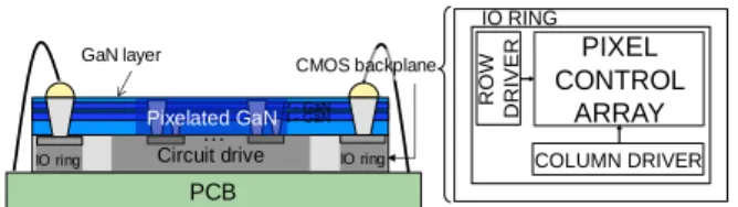
The microdisplay consists in an array of pixelated GaN micro-LED at 9.5µm pitch [10], stacked on top of a CMOS driving circuit (backplane), shown Fig. 1. Depending on final microdisplay application, GaN array can be monochrome green, for very high luminance need, or monochrome blue, combined with conversion layers to obtain a bicolor or a full color microdisplay. CMOS circuit configuration enables adapted polarization depending on desired color mode (see Fig. 1 and detailed CMOS architecture Fig. 7).
Last metal layer in CMOS circuit offers electrical connection in pixel for both anode and cathode. Anode is pixelated individually for each LED, whereas cathode is common for the whole microdisplay, and routed in grid on LED array die. PAD opening on GaN layer, above CMOS IO ring, enables a microdisplay external control, with an electrical connection from PCB to the circuit core via multiple bondings.
B. LED mismatch compensation
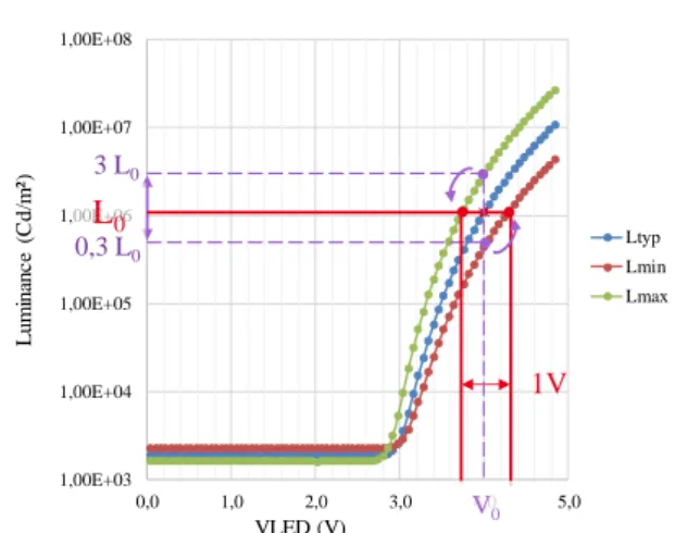
As mentioned earlier, GaN LED maturity level has some drawbacks. It can influence directly control circuit architecture. Typically, non-negligible process mismatch is an important concern. Then, it is necessary to apply an individual correction to each LED to ensure good luminance uniformity. Fig. 2.and Fig. 3 show performances from previous GaN µLED characterizations. Fig. 2 shows the
PCB N - GaN P - GaN GaN layer IO ring IO ring CMOS backplane Pixelated GaN Circuit drive … R O W D R IVER COLUMN DRIVER PIXEL CONTROL ARRAY IO RING
Fig. 1. GaN layer stack with CMOS backplane, and CMOS display circuit drive principle.
1,00E+03 1,00E+04 1,00E+05 1,00E+06 1,00E+07 1,00E+08 0,0 1,0 2,0 3,0 4,0 5,0 L u m in an c e (C d /m ²) VLED (V) Ltyp Lmin Lmax 1V 3 L0 L0 0,3 L0 V0
Fig. 2. Measured minimal, maximial and typical luminance versus µLED voltage for a 8µm pitch µLED
nominal voltage V0 for a goal luminance L0, and 10 times
min to max luminance error due to dispersion without correction, for the fixed V0.
On Fig. 3, nominal current induces 4 times min-max luminance error on a linear curve, easier to correct. Hence, current correction architecture is chosen. Current control is also a good solution for other emissive technology such as OLED. Evolution of electro-optical characteristics with increased temperature tend to deliver larger current for a constant voltage. Microdisplays with a voltage control will deliver more current, leading to circuit ageing, and could suffer from supply collapse, thus degrading microdisplay performance.
Assuming that luminance uniformity of 10% is not perceptible to human eye, we can deduce current correction range and accuracy. To ensure the 10% uniformity, we chose a harder correction specification of 5%. Then, a 5 bits current correction is enough for required luminance uniformity. Before normal use of microdisplay, a calibration phase will evaluate LED-to-LED dispersion with a 5 bits accuracy. The resulting 5bits mismatch picture will be stored in an external memory, and will define the pixel current polarization later, during a normal use.
C. Pixel Circuit
On the proposed pixel Fig. 4, the transistor P1 and P2 act as current sources. During current initialization, Fig. 5.a, P5 and P6 are turned ON, and P1 and P2 are diode connected. This configuration prevents from error copy due to voltage drop and threshold voltage variations of P1 and P2. According to 5 bits LED correction, a column foot DAC will provide the appropriate current IDAC through P1 and P2. At the end of initialization phase, voltage Vg(P1,P2) is
stored in P1 and P2 parasitic capacitor Cgs1 and Cgs2 .
In the meantime, a color data is written in the digital memory. To minimize pixel area, grey level information is expressed by binary mode PWM called BCM (for Binary Code Modulation), with an in pixel digital memory. During LED emission phase Fig. 5.b, LED is turned either ON or OFF depending on PWM current bit emission. For a logical ‘1’, LED will be turned ON, with a Luminance value L(IDAC).
During emission phase, LED to LED voltage variation on anode is expected, because of LED process variations. This
1,00E+03 1,00E+04 1,00E+05 1,00E+06 1,00E+07 1,00E+08
10E-10 01E-8 10E-8 01E-6 10E-6 01E-4
L u m in an c e (C d /m ²) ILED (A) Ltyp Lmin Lmax 1,5 I0 2 L0 0,5 L0 I0 L0
Fig. 3. Measured minimal, maximal and typical luminance versus µLED current for a 8µm pitch µLED.
may cause an unpredictable Vds(P1) and Vds(P2) variation
between initialization and emission phase, leading to current variations, and then luminance non uniformity. To minimize current error from drain to source voltage difference of P1 and P2, current source is cascoded.
Coarse adjustment of microdisplay global luminance is implemented directly in pixel with HIGHL_EN signal. When HIGHL_EN=’1’, both P1 and P2 are selected to deliver full current amplitude. When HIGHL_EN=’0’, only P2 current source is activated, and drives LED with a lower
current depending on P1 and P2 W/L ratio, given by:
Assuming current is linear with luminance, for a chosen high luminance level L0, lower luminance only depends on
P1 and P2 W/L ratio.
When HIGHL_EN=’0’, no current flows through P1. In this luminance mode, gate node voltage Vgs(P2) is highly
sensitive to variations (flicker or charge injection), because of small storage capacitor Cgs2 . Proposed pixel architecture
uses P1 as a MOS capacitor connected to gate current source Vg(P2) when HIGHL_EN=’0’. P2 gate is then loaded by a
bigger capacitor than Cgs(P2), and lowers gate sense node
Vg(P2) sensitivity to variations. GND VDD P1 P3 P2 P4 MEMORY Vcasc Vcasc Init_Current ID A C P5 P6 HIGHL_EN Cgs1 Cgs2 SPWM
GND VDD P1 P3 P2 P4 MEMORY ID A C Vcasc SPWM GND VDD P1 P3 P2 P4 Logical ‘1’ ID A C Vcasc SPWM
Fig. 5.a) Pixel current initialization phase, example with HIGHL_EN=’1’ Fig. 5.b) Pixel emission phase, example with HIGHL_EN=’1’
GND VDD P1 P4 Vcasc Cgs1 P2 Cgs2
Fig. 6. Pixel equivalent current source in low luminance mode (for HIGHL_EN = ‘0’)
D. Pixel layout
As discussed previously, high brightness microdisplay leads to an important amount of power delivered by CMOS control circuit. Then, power dissipation and voltage drop are both limiting microdisplay performance. Voltage drop will decrease locally supply headroom, and prevent current source from delivering the proper current value, resulting in a decreased luminance in micro-display’s center [9]. To mitigate those effects, pixel routing strategy consists in using thick metals and high-density metal routing in pixel. LED common cathode is also electrically connected to CMOS circuit in each pixel, and can benefit from the high density routing strategy, helping to minimize voltage drop. Final pixel pitch is 9.5µm (see Fig. 8).
E. Top architecture
CMOS driving circuit comprises a 1640x1033-pixel array of the presented pixel (see Fig. 4), and its integrated control electronics (see Fig. 7). Row driver acts as a rolling shutter control of the array, enabling row current initialization, memory initialization and micro-LED emission. Row driver also allows a precise dimming function via emission control with PWM switch. Color Data Driver addresses the appropriate color data to the corresponding column. Mismatch data Driver addresses column Current DACs by distribution of the appropriate 5 bits mismatch data to each column DAC.
Each column DAC consists in a 5 bits current steering DAC architecture, with unity current sources pondered depending
on DAC bit. DAC current IDAC derived from classical
current steering DAC formula is given by:
I0 is the minimal current per pixel, for a given color and
luminance mode. ILSB is the DAC unity current. i is the bit
weight for mismatch correction.
For example, with a monochrome green microdisplay with configuration HIGHL_EN=’1’, minimal current I0 is 5µA
with Datamismatch[4:0]=’00000’, and maximal current is 20µA, with Datamismatch[4:0]=’11111’.
Knowing that DAC to DAC current mismatch decreases when WxL of unity current source increases [11], design of DAC cell consisted in a tradeoff between DAC to DAC dispersion, and DAC affordable pitch. The DAC final footprint is 19µm x 80µm.
DAC BIAS cell controls the unity DAC current. According to COLOR_MODE[1:0], VBIAS[3:0] will impose same voltage to each VBIAS in monochrome mode, or different value for bicolor and full color mode. Selection of different color current references in DAC BIAS cell enables relative color modification via current ratio tuning. This enables color temperature adjustment, or correction of micro-LED wavelength shift from expected values.
Total circuit footprint is 20mm x 14.5mm (Fig. 8).
1640 X 1033
PIXEL array
5bit CURRENT DAC COLOR DATA DRIVER
R O W D R IV ER
MISMATCH DATA DRIVER
DAC BIAS Datacolor[1639:0] IN IT _ C U R R E N T [1 0 3 2 :0 ] W R IT E_ M EM O R Y[ 1 0 3 2 :0 ] IDAC[1639:0] Datamismatch[8199:0] V BI A S[ 3 :0 ] CLK, VSYNC HIGHL_EN COLOR_MODE[1:0] REF_COLOR_R[7:0] REF_COLOR_G[7:0] REF_COLOR_B[7:0] DATAMISMATCH[4:0] DATACOLOR[9:0]
Fig. 7. Top architecture of CMOS driving circuit.
20mm
14.5mm
15.58mm
9.82mm
Active matrix Core
Active matrix Control
T
EST
9,5µm PIXEL
III. RESULTS AND DISCUSSION
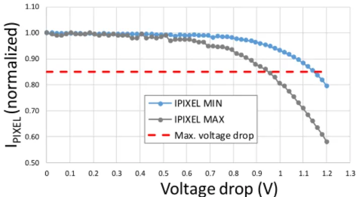
The curve of Fig. 9 shows the luminance versus supply voltage drop. Voltage drop affects particularly luminance drop for highest pixel current (equivalent to maximal mismatch correction). Under high currents, Vsg(P1) and
Vsd(P1) are more important and suffer from a lack of
headroom.
Voltage drop will cause current decrease, and affect luminance uniformity across the array. However, human eye is less sensitive to luminance gradient caused by voltage drop than pixel-to-pixel variation due to LED mismatch. Then, luminance uniformity specification is less constraint than for LED correction calculation, so 15% luminance loss is already acceptable. As soon as total voltage drop does not exceed 950mV, current decrease is under 15%, as well as luminance decrease. Expected voltage drop is 0.27V for ground supply and 0.24V for power supply. Total column voltage drop is 0.51V < 0.95V. Thus, the whole column can be turned ON with acceptable luminance loss due supply drop.
This is particularly interesting in avionics applications needing high contrast for displaying information or symbology.
Expected luminance for a fully ON monochrome green microdisplay with 20µA nominal current is 3.8MCd/m² [10].
Expected pixel performances are summarized TABLE I. .
TABLE I. PIXELSPECIFICATIONS
Pixel specification Expected results
Value Unit
Max. Brightness 3.8x10⁶ cd/m²
Pixel pitch 9.5 µm LED mismatch correction 5 bit Pixel current 5 to 20 µA Pixel voltage 5.5 V
IV. CONCLUSION
We report the design and fabrication of a CMOS control circuit for a future 1640x1033 array of GaN µLEDs. To our knowledge, this is the first circuit providing sufficient power to drive micro-LEDs array with a luminance level suitable for outdoor applications. With a monochrome green array of GaN micro-LED, we expect 3.8MCd/m², if the whole array is turned ON at highest luminance. Two analog luminance modes allow a coarse dimming. Thinner dimming adjustment is also possible via PWM duration control. Multi-color mode enables several emissive source nature, with different type of array: monochrome, bicolor, full color. Color temperature can also be adjusted depending on source nature and ageing. This versatile circuit enables multisource usage, and paves the way for further GaN micro-LEDs evolution. 0.50 0.60 0.70 0.80 0.90 1.00 1.10 0 0.1 0.2 0.3 0.4 0.5 0.6 0.7 0.8 0.9 1 1.1 1.2 1.3
I
PIX EL(n
o
rm
al
iz
ed
)
Voltage drop (V)
IPIXEL MIN IPIXEL MAX Max. voltage dropFig. 9.LED current delivered vs. Supply voltage drop
ACKNOWLEDGMENT
The author acknowledge funding from the CleanSky-H2020 European project (under H2020-EU.3.4.5.6-ITD Systems, Project ID: 755497).
REFERENCES
[1] V.Gohri et al., “High Brightness Green OLED Microdisplay With High Resolution and Low Power Consumption”, SID Conference
Record of the International Display research Conference, pp.81-84,
2011.
[2] Z.J.Liu,W.C.Chong,K.M.Wong, K.H.Tam, and K.M.Lau, “A Novel BLU-Free Full-Color LED Projector Using LED on Silicon Micro-Displays”, IEEE Photonics Technology letters, vol.25, no.23, pp.2267-2270, 2013.
[3] Z.J.Liu, K.M.Wong, C.W.Keung, C.W.Tang, and K.M.Lau, “Monolithic LED MicroDisplay on Active Matrix Susbstrate Using Flip-Chip Technology, IEEE Journal of Selected Topics in Quantum
Electronics, vol.15, pp.1298-1302, 2009.
[4] J.J.D.McKendry et al., « Individually Adressable AlInGaNMicro-LED Arrays With CMOS Control and SubNanosecond Output Pulses”, IEEE Photonics Technology Letters, vol.21, no.12, pp811-813, 2009.
[5] F.Templier et al., “High Brightness GaN LED Arrays Hybridized on Silicon Interconnect at a Pixel Pitch of 10µm”,Proceedings of the
International Display Workshops,pp.1279-1282,2014.
[6] H.S.El-Ghoroury,C.L. Chuang,Z.Y. Alpaslan, “Quantum Photonic Imager (QPI): A novel Technology That enables more than 3D Applications”, SID Symposium Digest of Technical Papers,vol.46, pp 371-374, 2015.
[7] F.Templier et al., “GaN based emissive microdisplays: A very promising technology for compact, ultra-high brightness display systems,’Journal of the Society for Information Display, vol.24, pp669-675, 2016.
[8] J.Day, J.Li, D.Y.C.Lie, C.Bradford, J.Y.Lin, H.X.Jiang, “III-Nitride full-scale high-resolution microdisplays”, Applied Physics Letters, vol.99, pp.031116-031116, 2011.
[9] J.Herrnsdorf et al., “Active-Matrix GaN Micro Light-Emitting-Diode Display with Unprecedent Brightness”, IEEE Transactions on
Electron Devices, vol.62, no.6, pp.1918-1925, 2015.
[10] E.Quesnel et al., “Dimensioning a full color LED micro-display for augmented reality headset in a very bright environment”,Journal of
the Society for Information Display, accepted, in press, 2020.
[11] B.Zhao et al., « An Accurate Current Scaling Circuit for Self-Emissive Microdisplay driving circuit », 2018 14th IEEE International
Conference on Solid-State and Integrated Circuit Technology, pp.1-3,
2018