HAL Id: hal-01741465
https://hal.laas.fr/hal-01741465
Submitted on 11 Apr 2018
HAL is a multi-disciplinary open access
archive for the deposit and dissemination of
sci-entific research documents, whether they are
pub-lished or not. The documents may come from
teaching and research institutions in France or
abroad, or from public or private research centers.
L’archive ouverte pluridisciplinaire HAL, est
destinée au dépôt et à la diffusion de documents
scientifiques de niveau recherche, publiés ou non,
émanant des établissements d’enseignement et de
recherche français ou étrangers, des laboratoires
publics ou privés.
Clément Arlotti, Gael Lafleur, Alexandre Larrue, Pierre-François Calmon,
Alexandre Arnoult, Guilhem Almuneau, Olivier Gauthier-Lafaye, Stéphane
Calvez
To cite this version:
Clément Arlotti, Gael Lafleur, Alexandre Larrue, Pierre-François Calmon, Alexandre Arnoult,
et al..
Coupled-mode analysis of vertically-coupled AlGaAs/AlOx microdisk resonators.
IEEE
Journal of Quantum Electronics, Institute of Electrical and Electronics Engineers, 2018, 54 (3),
�10.1109/JQE.2018.2811739�. �hal-01741465�
Abstract—This article reports the experimental and theoretical assessments of the optical characteristics of recently-introduced
vertically-coupled microdisk resonators made by selective oxidation of AlGaAs multilayer structures. Experimental measurements show that the Q-factors are in the 103 to 104 range for diameters ranging from 75 to 300 µm. To establish the origins of this limited performance a coupled-mode-theory-based model of the single-access-waveguide-coupled resonator system was developed. It includes features which are specific to oxide-based vertically-coupled resonators, namely losses towards the slab waveguide lying under the resonator and a coupling region with an asymmetric and multilayer structure. Setting this simulation tool required the proposal and validation of a general criterion to select an appropriate set of decomposition permittivity profiles to be able to accurately model the characteristics of these more complex couplers using the coupled-mode-theory approach. This theoretical development is generic and can be now deployed to simulate any device which includes multi-waveguide couplers with arbitrary piece-wise-constant profile of the dielectric permittivity. Exploiting this particular development and experimental measurements of the disk sidewall roughness and of the coupling lengths, the calculated and experimental Q-factors are found to be in good agreement and allow establishing that the current performance is limited by the scattering losses and the slab-leakage losses for small- and large-diameter devices respectively.
Index Terms— microresonators, coupled-mode analysis, integrated optics, optical waveguide components
I. INTRODUCTION
HISPERING-GALLERY-MODE resonators, in the form of micro-disks, rings or racetracks, have become a key building block in many high-performance photonic components [1][2][3] including high-purity spectral filters, low-threshold lasers and nonlinear converters, and high-sensitivity sensors. Embodiments using III-V semiconductors are particularly attractive since they allow active and passive sections to be integrated on the same photonic chip and broaden the range of achievable functions. In this context, the vertical integration of the resonator above its access waveguide(s) has several advantages over the lateral integration method where these elements are located side-by-side. Indeed, the former approach is considered to be technologically preferable for WGM resonators since in-situ reflectometry can be used to reliably and reproducibly control the device critical dimension, i.e. the separation between the resonator and its evanescently coupled input/output ports. Additionally, by allowing active and passive elements to be distributed in different planes, the vertical integration scheme offers a greater design and material flexibility as well as an easier fabrication route than would be achievable using respectively (quantum-well)-intermixing [4] or selective-area growth [5] lateral integration methods [6][7]. Practically, the vertical integration requires establishing a technological process flow leading to waveguide structures being defined in, at least, two different layers. To-date, there has been essentially three ways to do so. The first and most common approach relies on the planarization of an encapsulated etched waveguide followed by the definition of the upper etched waveguides (by deposition and etching [8][9], or by wafer-bonding separately-defined waveguides and removing their supporting substrate [10][11]). The second method uses a substrate transfer to be able to etch waveguides on both sides of a membrane structure [12]. The third technique exploits a localized oxidation to define the buried waveguide structure underneath the etched resonator [13][14]. The relative complexity associated with the above-described fabrication procedures has somewhat hindered the general uptake of the vertical integration scheme. Similarly, there is limited number of reports dealing specifically with the simulation of vertically-coupled resonators. Explanations for this fact can be traced back to a relative lack of experimental data, but also to the greater simulation complexity
Manuscript received 14/11/2017; accepted. Date of publication ; date of current version XX/XX/2018.
This work has been supported by the French Space Agency (CNES), by the DGA and by Renatech, the French network of microfabrication facilities. C. Arlotti, G. Lafleur, A. Larrue, P.-F. Calmon, A. Arnoult, G. Almuneau O. Gauthier-Lafaye and S. Calvez are with CNRS, LAAS, 7 avenue du colonel Roche, F-31400 Toulouse, France and with Univ de Toulouse, UPS, LAAS, F-31400 Toulouse, France (e-mail: [email protected])
A. Larrue is now with III-V Lab, Campus de Polytechnique, 1, avenue Augustin Fresnel , RD128, F-91767 Palaiseau Cedex (e-mail: [email protected])
G. Lafleur is now with AET Technologies, 8 chemin de malacher, Inovallée, 38240 Meylan, France.
Coupled-mode analysis of vertically-coupled
AlGaAs/AlOx microdisk resonators
Clément Arlotti, Gaël Lafleur, Alexandre Larrue, Pierre-François Calmon, Alexandre Arnoult,
Guilhem Almuneau, Olivier Gauthier-Lafaye and Stéphane Calvez
characteristics even over wide spectral spans [15][16][17][18]. In particular, such simulation tool has permitted to emphasize that, for microring or microdisk resonators that are vertically-coupled to straight access-waveguides, the coupling is not point-like as for laterally-coupled devices but does occur over an extended length and, as a result, bears a significant influence on the resulting spectral characteristics [17][18].
In this paper, following our recent extension of the use of selective lateral oxidation [19][20] to create vertically-coupled microdisk resonators on an (Al)GaAs platform [14], we provide a more extensive set of experimental characterization results. Additionally, the device performances are quantitatively analyzed using a CMT-based model taking into account the specificities of this embodiment namely a slab-waveguide loss channel and an asymmetric multi-layer separation between the access and resonator waveguides. As an integral part of the here-described modelling work, we establish a method to perform the critical step ensuring an accurate CMT treatment of the coupling region which is to decompose the multilayer asymmetric coupler into a set of individual constitutive elements. To address all these points, the manuscript is organized into five sections. In the first part, the device structure layout is described together with the assessment of the resonator quality factor as a function of microdisk diameter and relevant information regarding the microdisk sidewall rugosity and coupler length evaluation. The CMT model is presented in detail in the second section whilst the loss and coupling parameters are evaluated numerically in the following two sections. Finally, the numerical results are confronted with the recorded experimental data in the last part of the manuscript.
II. DEVICE STRUCTURE AND EXPERIMENTAL RESULTS
The vertically-coupled AlGaAs/AlOx microdisk resonators under study have been introduced and described in detail, including their fabrication, in [14]. The device layout and operation principle can be inferred from the microscope image and simplified cross-sectional view provided in Fig. 1. As shown, the structure can be divided into two regions: a disk section of chord length, L, where the 680-nm-thick-GaAs-core resonator lies above an access waveguide (materialized by the pink region where the 68nm-thick Al0.98Ga0.02As layers are still unoxidized) and the remainder of the disk which is separated from a GaAs-slab waveguide by an Al0.3Ga0.7As (100 nm)/AlOx (63 nm)/ Al0.3Ga0.7As (330 nm)/ AlOx (63 nm)/ Al0.3Ga0.7As (150 nm) multilayer. The change in thickness (from 68 nm to 63 nm) between the Al0.98Ga0.02As and AlOx layer is the result of the conventionally-observed volumic contraction occurring during the oxidation process [21][22].
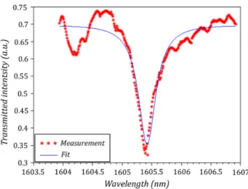
Experimental intensity transmission spectra under TE-excitation were recorded using a step-tunable laser with a central wavelength of 1.6 μm, a 10-pm spectral resolution and a 100-kHz linewidth. As shown in [14], the devices sustain two radial families of modes. Individual resonances of the fundamental modes were subsequently fitted with Lorentzian curves as shown in Fig. 2, displaying loaded quality-factors of the order of Q~103 to 104 (see Fig. 8).
As the device response is set by the interplay between the access-waveguide-to-resonator coupling and the resonator loss level, further experimental information is needed to be in a position to reproduce the above-presented results.
Fig. 1. (left) Microscope top-view image with superimposed mode propagation paths (red and orange dashed arrows) [12] and (right) cross-sectional schematic of the vertically-coupled microdisks. The green arrows represent the coupling between the oxide-confined access waveguide and the resonator whilst the orange arrow indicates the resonator mode leakage to the slab waveguide. 680nm GaAs 68nm Al 0,98Ga0,02As 63nm AlOx Al0,3Ga0,7As 480nm GaAs Al0,6Ga0,4As GaAs substrate L
The first useful experimental parameter to measure is therefore the coupling (chord) length, L, since it controls the amount of light coupled between the access waveguide and the resonator (and vice-versa) and, most importantly, since it strongly depends on the alignment between the lithographic steps which successively defines the access and resonator waveguides. As shown in Fig. 1, this coupling length, L, can be directly quantified from the optical microscope images of the devices. The evolution of this parameter as a function of diameter of the fabricated microdisks is represented in Fig. 3.
Furthermore, since a source of optical loss in the resonator originates from the roughness of its etched sidewall, scanning-electron microscope (SEM) images of the microdisk periphery were taken to evaluate it. As Fig. 4 shows, the etch quality (smoothness) worsens with increasing etch depth, a commonly observed result when fabricating devices by dry etching [23]. After post-processing the images using a Canny-filter edge-detection [24] and performing the statistical analysis as commonly done for line edge roughness analysis [25], the etched sidewall is found to exhibit a 19.6-nm-rms roughness with a ~503 nm correlation length. It should be pointed out that the latter value is consistent with the laser (400 nm x 800 nm) spot-size used to perform the photolithography steps.
III. MODEL OF THE WAVEGUIDE-COUPLED RESONATORS
The analysis carried out here is based on the universal description of a resonator coupled to a single access waveguide [26]. As it will be described in full in section V, the behavior in the evanescent coupling section of length L (see Fig. 1) is treated using the complete Coupled-Mode Theory (CMT) as in references [18] and [27]. The assumption made here is that bothf the resonator and access waveguides are each taken to only support one single transverse mode. In this case, the intensity transmission T characteristic recorded at the exit of the access waveguide is given by:
Fig. 2. Measured transmission characteristic of a 75-µm-diameter microdisk resonator and associated Lorenzian fit showing a Q-factor of 4610 ± 374
Fig. 3. Measured coupling (chord) lengths of the fabricated microdisks.
Fig. 4. Typical SEM image of the sidewall of a 75µm-diameter microdisk used for roughness analysis.
Inner part of the disk
Outside of the disk
where t is the amplitude transmission coefficient of the codirectional coupler, a represents the single-pass transmission coefficient of the resonator and ϕ is the single-pass round-trip phase accumulated over the total length of the resonator, LR. The latter parameter is expressed as follows:
𝜑 = 𝛽𝑅(𝐿𝑅− 𝐿) + 𝜙𝑡 (2)
βR being the effective propagation constant in the resonator, and ϕt the complete-CMT phase-shift introduced by the coupler. The device transmission response can be approximated as a set of Lorentzian dips separated by the cavity free spectral range. The full-width at half maximum of these dips, Δλ, is related to the resonator loaded quality factor, Q, whose expression is:
𝑄 =Δλλ =�𝑎|t|(𝛽𝑅(𝐿𝑅−𝐿)+𝜙𝑡)
2(1−𝑎|t|) (3)
To be able predict and analyze the behaviour of the coupled resonator, this model requires the evaluation of the two parameters a and t, i.e. of the internal and external loss rates. This is the object of the following two sections.
IV. LOSS-RATE EVALUATION
The internal loss rate of the resonator, a, is usually calculated from the intensity loss propagation rate, ρ, averaged over the whole length of the resonator, LR, using the following relationship [28]:
𝑎 = 𝑒− 𝜌2𝐿𝑅 (4)
Here, the resonator losses are assumed to originate from three different contributions:
ρ=ρbend+ ρslab+ρscatter (5)
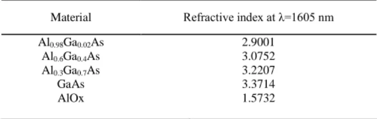
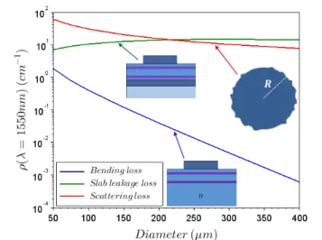
where ρbend represents the bending loss rate, ρscatter represents the scattering losses due to roughness of the disk edge and ρslab represents the loss rate due to coupling of the resonant cavity modes to leaky modes supported by the underlying slab waveguide. The resonator-mode effective propagation constant, βR, bending and slab leakage losses were obtained from the finite-difference open-source programme Wgms3d [29], by extracting the real and imaginary parts of the TE-polarized fundamental mode complex effective index, calculated for the two different structures whose cross sections are represented on Fig. 5. The material refractive indexes used for these calculations are taken to follow the wavelength-dependent expressions provided in [30][31] and a list of the values at a wavelength of 1605 nm is summarized in Table 1 for completeness. We note that the trapezoidal mesa opening (see Fig. 1) was not taken into account in the above-mentioned calculations as it was deemed to be sufficiently far away from the disk edge to induce negligible additional loss to the considered tightly-confined fundamental radial modes. When comparing the mode profiles resulting from the simulations without (bend loss calculation) and with the leakage slab (leakage loss calculation), the mode profile is found to essentially shift downwards in the presence of the leakage slab. As a result, the bending losses are taken to be identical in both scenarios and the extracted leakage losses are obtained after subtraction of the bending losses as calculated in the absence of the slab. This might lead to a slight over-estimation of the slab leakage losses but not of the combined loss level.
Finally, the resonator scattering losses due to sidewall roughness were calculated from an analytical approximation of the volume current method quality factor, Qss, corresponding to surface scattering of TE-modes of the disk [32] using the experimental roughness values determined in section II. This allowed us to compute the scattering loss rate ρscatter=βR/Qss shown in Fig. 5 (red curve). As expected, this contribution is a decreasing function of the disk diameter. Indeed, with increasing disk diameter, the confinement of the fundamental whispering-gallery mode improves (as βR increases), and the interaction of this optical field with the vertical sidewall imperfections weakens.
Straightforward analysis of Fig. 5 reveals that, should the internal losses be the dominating source of loss, the devices gradually change from being scattering-loss-limited for small diameters to slab-leakage-limited at large diameters.
TABLEI USED REFRACTIVE INDEXES
Material Refractive index at λ=1605 nm
Al0.98Ga0.02As 2.9001 Al0.6Ga0.4As Al0.3Ga0.7As GaAs AlOx 3.0752 3.2207 3.3714 1.5732
V. COUPLING-RATE ASSESSMENT
The second element required to be in a position to analyze the device performance is the coupling-rate. Here, we follow a standard coupled-mode description [33]. For a coupler made of two parallel waveguides of length, L, the coupling-rate, t, is given by:
t = cos(Г𝐿) + 𝑗𝛿�Гsin(Г𝐿) = |t|𝑒−𝑖𝜑𝑡 (6) with the wavevector of the power transfer oscillations given by:
Г = �κ𝑎κ𝑏+ 𝛿̂2 (7)
In the latter expression, κa and κb are the reduced form of the mode-overlap integrals and 𝛿̂ represents the complete-CMT effective propagation constant mismatch. The latter parameter is given by:
δ� =βwg-βR
2 +
αa-αb
2 (8)
where αa and αb are the complete-CMT self-coupling coefficients, i.e corrections induced by the coupling interaction to the propagation constants of the isolated waveguide and resonator (respectively βwg and βR).
The expressions for the reduced coupling coefficients appearing in (8)-(9), are 𝜅𝑎=𝜅121−|𝑐−𝑐1212𝜅|222 (9) 𝜅𝑏=𝜅21−𝑐12∗ 𝜅11 1−|𝑐12|2 (10) 𝛼𝑎=𝜅121−|𝑐𝑐1212−𝜅|211 (11) 𝛼𝑏=𝜅21𝑐12 ∗ −𝜅22 1−|𝑐12|2 (12) where κkm= ωε0∬�ε-εm� Em∙ Ek*dxdy, (13)
represent the evanescent coupling coefficients from waveguide m to waveguide k (with k=1,2 and m=1,2 here) and quantify how efficiently the power transfers between the two parallel waveguides. For reference, the y-axis was taken to be the vertical axis with its origin set at the top of the disk and pointing towards the substrate. Since the analysis is carried out for vertically-stacked slab waveguides, the x-axis location is irrelevant.
The butt-coupling coefficients, ckm, are given by:
ckm= ∬ ez. �Em× Hk* + Ek* × Hm�dxdy (14)
They represent the excitation efficiency from a field propagating into a waveguide with an eigen-modes basis {Em(x, y)} to a field propagating into a waveguide with an eigen-modes basis{Ek(x, y)}, �Em,k(x, y)�being the transverse mode profiles of the individual isolated waveguides.
As we will show hereafter, a crucial step in this type of CMT calculations is, given the coupler overall permittivity distribution,
ε, to define an appropriate set of individual decomposition permittivity profiles, εm, (and associated set of mode basis{Em(x, y)}) in order to be able to accurately calculate the above-defined coefficients and the coupler associated characteristics. In most cases, as when the coupler is made of two laterally-coupled waveguides, the choice of the isolated waveguide distributions is straightforward. However, for couplers with an asymmetric multilayer permittivity profile, as relevant for the device structures considered here, this task becomes less obvious but is, nevertheless, often ambiguous in the relevant literature [34]–[36]. Using
Fig. 5. Evolution of calculated loss rate with microdisk diameter for the various types of internal losses.
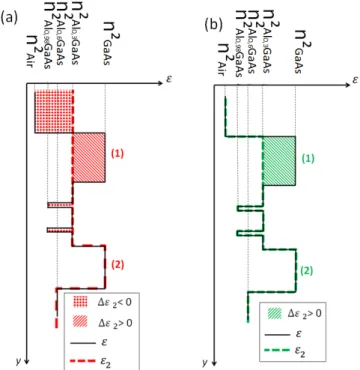
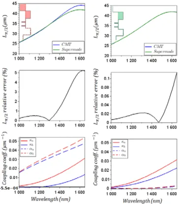
The overall permittivity profile of the considered vertical coupler is depicted in Fig. 6. The proposed selection process relies on choosing the individual permittivity distributions, εm, such that, on each piece of the distribution, the value of the difference Δεm=ε-εm is either positive or null and as small as possible, in order to best fit the perturbative nature of the CMT and thereby ensure the accuracy of the results. Moreover, εm is chosen such that the permittivity perturbation value Δεm is minimized, positive and non-zero only in the core region of waveguide k, and zero everywhere else. This way, the integration domain is restricted to the latter waveguide core and it becomes easier to understand that κkm is the evanescent field overlap leading to a guided power transfer from waveguide m to the core of waveguide k.
Due to the simplicity of deriving their eigen-modes, 3-layer slab-like individual permittivity decompositions are often proposed as alternatives to multilayer (>3 layer) decompositions in the relevant litterature [34]–[36]. At this stage and as shown in Fig. 6, it is worth pointing out that the resulting Δεm is, in this case, no longer piece-wise minimized as it presents larger variations from ε than the proposed multilayer decomposition.
To compare these two sets of decompositions, the reduced coupling coefficients and the coupler beat-length, Lπ/2, which is the required coupler length to obtain the maximum transfer of power from one guide to the other, are calculated for these two cases. With the CMT approach, the coupler beat-length is given by [33]:
𝐿𝜋/2 =2𝛤𝜋 (15)
However, the coupler behaviour can also be analyzed in terms of the supermodes of the structure. The latter modes, also called array modes, are the modes supported by the complete multilayer stack of the coupler. Neglecting the higher order modes, the total electric field of the coupler can be understood to result from the interference effect between the first two supermodes (respectively even and odd supermodes) and the coupler beat-length can thus be expressed as:
𝐿𝜋/2=𝛽𝑒−𝛽𝜋 𝑜 (16)
where βe and βo are the propagation constants of the even and odd supermodes respectively.
Fig. 7 displays the reduced form of the mode overlap coupling coefficients yielded by the individual permittivity decompositions described in Fig. 6 and computed with the corresponding one-dimensional vertical field overlap integrals. It highlights the importance of the permittivity decomposition criterion. As shown in the topmost panels of Fig. 7, a first observation is that the Lπ/2 calculated using the supermode and CMT decomposition exhibits larger differences (especially at long wavelengths) when using a 3-layer decomposition rather than the proposed multilayer decomposition. As attested in the middle panel (left and right), the accuracy in the Lπ/2 evaluation is, at least, an order of magnitude better with the proposed multilayer CMT decomposition and, therefore, justifies favoring the latter decomposition. It also turns out that Fig. 7 (bottom left) also demonstrates that the 3-layer decomposition is in fact inadequate for the two reasons. First and foremost, the values of the self-coupling coefficients (αa,b) are greater than the mutual-coupling coefficients κa,b, a result inconsistent with standard CMT predictions since the latter parameters describe the primary source of the power exchange in the coupler and the former only
Fig. 6. Coupled-mode theory decomposition using (a) a 3-layer structure (b) a multi-layer structure derived from the proposed selection criterion.
represent second-order effects. Additionally, the coefficient κb is seen to be null at a wavelength close to 1250 nm, whilst κa remains positive. This zero value of κa originates from the fact that the one of the decomposition profiles leads Δεm to have regions with both positive and negative values (respectively inside and outside of the core of waveguide k) which, in turns (upon the integration over the entire set of regions), leads to an artificial and dubious absence of power transfer from waveguide m to waveguide k. On the contrary, the right panel of Fig. 7 shows that the multi-layer permittivity decompositions described in Fig. 6, which follows our selection criterion, is free from the above-mentioned shortcomings and enables a much more accurate estimation of the coupler beat-length. It is therefore this decomposition which was used in the remainder of this work for the evaluation of the coupler and device characteristics.
VI. MODEL VALIDATION
Having derived all the necessary elements, the Q-factor of the experimentally-fabricated vertically-coupled micro-disk resonators was evaluated as a function of their diameter, D. As described above and as in [15][16][17][18], the coupler characteristics were computed using a one-dimensional (vertical) CMT analysis of the coupler. The coupling length, L, was considered to follow:
𝐿 = 2�(𝑊 − 𝑋0)(𝐷 + 𝑋0− 𝑊) (17)
with W being the width of the oxide aperture and, X0 a fixed lateral offset. Their values (W=5.3 µm, X0=1.6 µm) were obtained by fitting the measured coupling lengths shown in Fig. 3.
Fig. 7. Coupler characteristic coefficients derived from (left) a 3-layer decomposition structure, (right) the proposed multilayered decomposition. The Lπ/2 error is established by comparison to the value derived from the supermode analysis of the coupler.
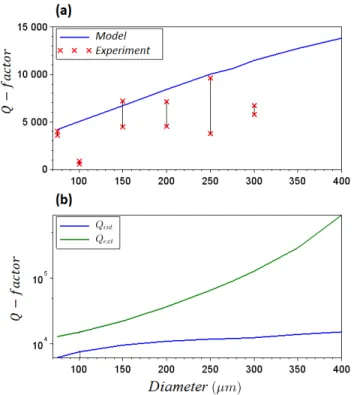
The direct comparison between the measured (on 50 resonances per diameter point) and calculated Q-factors is shown in Fig. 8 (a). Given that the model only relies on experimentally-inferred parameters, does not include any adjustable parameter nor coupling to higher-order radial modes (which do experimentally exist – see Fig. 2), the fact that the simulated Q-factors lie at the upper level of their corresponding experimentally-inferred values (except for the 300µm-diameter devices) is considered as achieving a good agreement between the modelled and experimental datasets. Unravelling the different loss contributions from the modelled Q-factors, the device performance is established to be limited by the internal and not the external (access-waveguide-coupling-only) losses (see Fig. 8(b)). In light of this and of Fig. 5, the current device limitation is thus the leakage to the underlying slab waveguide for large diameter devices and the disk sidewall scattering losses for small diameter devices.
VII. CONCLUSION
In this paper, we have reported further experimental characterization of vertically-coupled microdisk resonators fabricated by selective oxidation of AlGaAs structures. A quantitative analysis of the measured quality factors was also performed using a model including the evaluation of the slab-waveguide loss inherent to these devices and a full coupled-mode-theory (CMT) treatment of the coupler. The device performance was shown to be limited by the internal losses whose dominant contribution was estimated to be the scattering losses for the small diameter resonators and the slab-waveguide loss for the larger microdisks. Since the scattering losses could be reduced with an improved etching procedure [37], the key to obtain higher quality factors will be a modification of the structure vertical layout to lower the leakage of the optical field into the underlying slab waveguide, which could be effectively achieved using designs with thicker oxide layers and/or mismatched waveguides. Furthermore, as part of the model development, a clarification of the method to select appropriate decomposition permittivity profiles to perform accurate CMT simulations of asymmetric and multilayer couplers was proposed and validated, thereby simplifying its use to analyze the optical characteristics of all kinds of coupler-based devices.
ACKNOWLEDGMENT
C. Arlotti thanks the French Space Agency (CNES) and the Direction Générale de l’Armement (DGA) for financial support of his PhD.
REFERENCES
[1] Matsko, A. B.., Ilchenko, V. S., “Optical resonators with whispering gallery modes I: basics,” IEEE J Sel Top Quantum Electron 12(1), pp. 3–14, 2006. Fig. 8. (a) Comparison between the calculated and measured Q-factors.
The red crosses correspond to the standard deviation limits extracted on 50 resonances. (b) Calculated internal (bending, substrate leakage and scattering) and external (coupling) contributions of the resonator losses.
[2] Ward, J.., Benson, O, “WGM microresonators: sensing, lasing and fundamental optics with microspheres,” Laser Photonics Rev. 5(4), pp. 553–570, 2011.
[3] Feng, S., Lei, T., Chen, H., Cai, H., Luo, X.., Poon, A. W, “Silicon photonics: from a microresonator perspective,” Laser Photonics Rev. 6(2), pp. 145–177, 2012.
[4] W. D. Laidig et al., “Disorder of an AlAs-GaAs superlattice by impurity diffusion,” Appl. Phys. Lett., vol. 38, no. 10, pp. 776–778, May 1981. [5] E. Tokumitsu, Y. Kudou, M. Konagai, and K. Takahashi, “Molecular beam epitaxial growth of GaAs using trimethylgallium as a Ga source,” J. Appl.
Phys., vol. 55, no. 8, pp. 3163–3165, Apr. 1984.
[6] M. Smit et al., “An introduction to InP-based generic integration technology,” Semicond. Sci. Technol., vol. 29, no. 8, p. 083001, Jun. 2014. [7] L. Hou and J. H. Marsh, “Photonic Integrated Circuits Based on Quantum well Intermixing Techniques,” Procedia Eng., vol. 140, pp. 107–114, 2016. [8] S. Suzuki, K. Shuto, and Y. Hibino, “Integrated-optic ring resonators with two stacked layers of silica waveguide on Si,” Photonics Technol. Lett. IEEE,
vol. 4, no. 11, pp. 1256–1258, 1992.
[9] M. Ghulinyan, R. Guider, G. Pucker, and L. Pavesi, “Monolithic Whispering-Gallery Mode Resonators With Vertically Coupled Integrated Bus Waveguides,” IEEE Photonics Technol. Lett., vol. 23, no. 16, pp. 1166–1168, Aug. 2011.
[10] K. Djordjev, Seung-June Choi, Sang-Jun Choi, and P. D. Dapkus, “High-Q vertically coupled InP microdisk resonators,” IEEE Photonics Technol. Lett., vol. 14, no. 3, pp. 331–333, Mar. 2002.
[11] F. Mandorlo, P. Rojo Romeo, J.-M. Fedeli, H. MD Sohrab, and R. Orobtchouk, “Mode Density Reduction and Coupling in Microdisk LASERs Processed on a 200-mm CMOS Pilot Line,” IEEE Photonics Technol. Lett., vol. 23, no. 17, pp. 1183–1185, Sep. 2011.
[12] P. P. Absil, J. V. Hryniewicz, B. E. Little, F. G. Johnson, and K. J. Ritter, “Vertically Coupled Microring Resonators Using Polymer Wafer Bonding,”
IEEE Photon. Techno. Lett., pp. 49–51, Jan-2001.
[13] P. Koonath, T. Indukuri, and B. Jalali, “Vertically-coupled micro-resonators realized using three-dimensional sculpting in silicon,” Appl. Phys. Lett., vol. 85, no. 6, p. 1018, 2004.
[14] S. Calvez et al., “Vertically Coupled Microdisk Resonators Using AlGaAs/AlOx Technology,” IEEE Photonics Technol. Lett., vol. 27, no. 9, pp. 982– 985, May 2015.
[15] F. Mandorlo, P. Rojo Romeo, X. Letartre, R. Orobtchouk, and P. Viktorovitch, “Compact modulated and tunable microdisk laser using vertical coupling and a feedback loop,” Opt. Express, vol. 18, no. 19, pp. 19612–19625, 2010.
[16] M. Ghulinyan et al., “Oscillatory Vertical Coupling between a Whispering-Gallery Resonator and a Bus Waveguide,” Phys. Rev. Lett., vol. 110, no. 16, p. 163901, Apr. 2013.
[17] F. Turri, F. Ramiro-Manzano, I. Carusotto, M. Ghulinyan, G. Pucker, and L. Pavesi, “Wavelength Dependence of a Vertically Coupled Resonator-Waveguide System,” J. Light. Technol., vol. 34, no. 23, pp. 5385–5390, Dec. 2016.
[18] C. Arlotti, O. Gauthier-Lafaye, A. Monmayrant, and S. Calvez, “Achromatic critically coupled racetrack resonators,” J. Opt. Soc. Am. B, vol. 34, no. 11, p. 2343, Nov. 2017.
[19] J. M. Dallesasse, N. El-Zein, N. Holonyak, K. C. Hsieh, R. D. Burnham, and R. D. Dupuis, “Environmental degradation of Al x Ga 1− x As-GaAs
quantum-well heterostructures,” J. Appl. Phys., vol. 68, no. 5, pp. 2235–2238, Sep. 1990.
[20] J. M. Dallesasse and N. Holonyak, “Oxidation of Al-bearing III-V materials: A review of key progress,” J. Appl. Phys., vol. 113, no. 5, p. 051101, 2013. [21] T. Takamori, K. Takemasa, and T. Kamijoh, “Interface structure of selectively oxidized AlAs/GaAs,” Appl. Phys. Lett., vol. 69, no. 5, pp. 659–661, Jul.
1996.
[22] K. D. Choquette et al., “Selective oxidation of buried AlGaAs versus AlAs layers,” Appl. Phys. Lett., vol. 69, no. 10, p. 1385, 1996.
[23] J. W. Bae et al., “Characterization of sidewall roughness of InP/InGaAsP etched using inductively coupled plasma for low loss optical waveguide applications,” J. Vac. Sci. Technol. B Microelectron. Nanometer Struct., vol. 21, no. 6, p. 2888, 2003.
[24] J. Canny, “A Computational Approach to Edge Detection,” IEEE Trans. Pattern Anal. Mach. Intell., vol. PAMI-8, no. 6, pp. 679–698, Nov. 1986. [25] C. Shin, “Line Edge Roughness (LER),” in Variation-Aware Advanced CMOS Devices and SRAM, vol. 56, Dordrecht: Springer Netherlands, 2016, pp.
19–35.
[26] A. Yariv, “Universal relations for coupling of optical power between microresonators and dielectric waveguides,” Electron. Lett., vol. 36, no. 4, pp. 321– 322, 2000.
[27] C. Arlotti, G. Almuneau, O. Gauthier-Lafaye, and S. Calvez, “Coupled mode analysis of micro-disk resonators with an asymmetric-index-profile coupling region,” in Photonics West 2017, 2017, vol. Proc. of SPIE Vol. 10090 100901D-1.
[28] A. E. Siegman, Lasers. Mill Valley, California: University Science Books, 1986.
[29] M. Krause, “Finite-Difference Mode Solver for Curved Waveguides With Angled and Curved Dielectric Interfaces,” J. Light. Technol., vol. 29, no. 5, pp. 691–699, Mar. 2011.
[30] M. A. Afromowitz, “Refractive index of Ga1−xAlxAs,” Solid State Commun., vol. 15, no. 1, pp. 59–63, Jul. 1974.
[31] K. J. Knopp, R. P. Mirin, D. H. Christensen, K. A. Bertness, A. Roshko, and R. A. Synowicki, “Optical constants of (Al0.98Ga0.02)xOy native oxides,”
Appl. Phys. Lett., vol. 73, no. 24, pp. 3512–3514, Dec. 1998.
[32] M. Borselli, T. J. Johnson, and O. Painter, “Beyond the Rayleigh scattering limit in high-Q silicon microdisks: theory and experiment,” Opt. Express, vol. 13, no. 5, p. 1515, 2005.
[33] K. Okamoto, Fundamentals of optical waveguides. San Diego: Academic Press, 2000.
[34] R. Stoffer, K. R. Hiremath, M. Hammer, L. Prkna, and J. Čtyroký, “Cylindrical integrated optical microresonators: Modeling by 3-D vectorial coupled mode theory,” Opt. Commun., vol. 256, no. 1–3, pp. 46–67, Dec. 2005.
[35] A. Hardy and W. Streifer, “Coupled mode theory of parallel waveguides,” J. Light. Technol., vol. 3, no. 5, pp. 1135–1146, 1985.
[36] Little, Brent E., and W. P. Huang, “Coupled-mode theory for optical waveguides.,” Progress In Electromagnetics Research 10, pp. 217–270, 1995. [37] G. A. Porkolab, P. Apiratikul, B. Wang, S. H. Guo, and C. J. K. Richardson, “Low propagation loss AlGaAs waveguides fabricated with plasma-assisted
![Fig. 1. (left) Microscope top-view image with superimposed mode propagation paths (red and orange dashed arrows) [12] and (right) cross-sectional schematic of the vertically-coupled microdisks](https://thumb-eu.123doks.com/thumbv2/123doknet/14259417.489135/3.918.272.639.714.867/microscope-superimposed-propagation-sectional-schematic-vertically-coupled-microdisks.webp)
![[PDF] Formation à ActionScript 2.0 dans Flash | Cours informatique](data:image/gif;base64,R0lGODlhAQABAIAAAP///wAAACH5BAEAAAAALAAAAAABAAEAAAICRAEAOw==)