HAL Id: hal-00384223
https://hal.archives-ouvertes.fr/hal-00384223
Submitted on 14 Mar 2020
HAL is a multi-disciplinary open access
archive for the deposit and dissemination of sci-entific research documents, whether they are pub-lished or not. The documents may come from teaching and research institutions in France or
L’archive ouverte pluridisciplinaire HAL, est destinée au dépôt et à la diffusion de documents scientifiques de niveau recherche, publiés ou non, émanant des établissements d’enseignement et de recherche français ou étrangers, des laboratoires
Paving the way for multiple applications for the
3D-AFM technique in the semiconductor industry
J. Foucher, E. Pargon, M. Martin, S. Reyne, C. Dupré
To cite this version:
J. Foucher, E. Pargon, M. Martin, S. Reyne, C. Dupré. Paving the way for multiple applications for the 3D-AFM technique in the semiconductor industry. SPIE 2008, 2008, San Jose, United States. pp.6922, �10.1117/12.772675�. �hal-00384223�
Paving the way for multiple applications for the 3D-AFM technique
in the semiconductor industry
J.Fouchera, E.Pargonb M.Martinb, S.Reynea, C.Dupréa,c
a
CEA-LETI-MINATEC, 17 avenue des Martyrs, 38054 Grenoble Cedex 9, France [email protected] b
LTM/CNRS, 17 avenue des Martyrs, 38054 Grenoble Cedex 9, France c
IMEP-LAHC, INPG-MINATEC
The 3D-AFM technique is a very well known technique as a non destructive reference to calibrate CD-SEM and Scatterometry metrology. However, recent hardware, tip design and tip treatment improvements have offered to the technique new capabilities that pave the way for multiple applications in the semiconductor industry. The 3D-AFM technique is today not only a calibrating technique but also a process control technique that can be use either at the R&D level or in fab environment.
In this paper, we will address the limits of the 3D-AFM technique for the semiconductor industry depending on the applications by focusing our study on tip to sample interactions. We will identify, test and validate potential industrial solutions that could extend the 3D-AFM potentialities. Subsequently, we will show some interesting applications of the technique related to LER/LWR transfer during silicon gate patterning and related to advance multiwires devices fabrication.
Keywords: CD, 3D-AFM, tip wear, interaction, capabilities, accuracy, LER, LWR
1. INTRODUCTION
The 3D-AFM technique is a derived technique from conventional and very well-known AFM technique1 . The discovery of the AFM technique in 1986 by Binnig, Quate and Gerber, has demonstrated the capability of the technique to investigate conductive and insulator materials with high sensitivity to measure forces as small as 10-18N and based on tunneling detection of the lever deflection. Since then, many improvements have been done related to this technique. Martin and Wickramasinghe demonstrate the capability of the AFM technique to investigate surfaces with high sensitivity based on optical detection of the lever deflection2. It is only in 1994 that Martin and Wickramasinghe
invented the CD-AFM3 and demonstrate the capability of the technique to image pattern sidewall through the
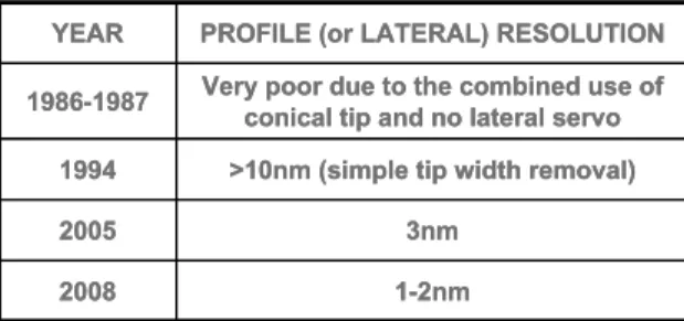
combination use of flared silicon tip and local surface slope detection in 2 dimensions. Afterwards, we had to “wait” until 2005 in order to see high order tip effects that are taken into account during tip shape extraction4 after measuring the pattern. In 2007, scan enhancements have lead the CD-AFM technique to really become the 3D-AFM technique by reducing drastically the sidewall noise level and by removing the notching data artifact at the bottom of measured patterns5. As an immediate result, the lateral resolution (or profile resolution) of the technique has reached today the nanometer level6 (cf. figure 1).
Today, there is a special need for accuracy in most of the semiconductor industry fields. Indeed, the continuous scaling down of patterns has reached such level that conventional industrial CD metrology techniques (such as CD-SEM and Scatterometry…) are very challenged in term of accuracy.
Therefore, CD metrology tool suppliers request for accurate tool calibration and the semiconductor industry increasingly requests also for accuracy in their production CD standards (golden wafers) calibration and requests for accuracy in their process development metrology such as OPC control, process window determination based on FEM (…). The 3D-AFM technique has a key role to play in order to fulfill on time advanced roadmap recommendations in order to reduce R&D and Production costs. The success of the 3D-AFM technique relies on its ability to reach sub-1nm accuracy. This level of accuracy relies on: 1- Scanning code enhancement; 2- Servoing quality; 3- Tip design;
4-Tip shape characterization; 5- Tip shape extraction and 6: Tip wear control.
1-2nm 2008
3nm 2005
>10nm (simple tip width removal) 1994
Very poor due to the combined use of conical tip and no lateral servo 1986-1987
PROFILE (or LATERAL) RESOLUTION YEAR
1-2nm 2008
3nm 2005
>10nm (simple tip width removal) 1994
Very poor due to the combined use of conical tip and no lateral servo 1986-1987
PROFILE (or LATERAL) RESOLUTION YEAR
Figure 1: Profile resolution or lateral resolution evolution of the AFM technique
Standing waves
= A /2 n Dense trench I 3 (2*1 574 57.6cc s=*d!*9
65mm Ieplaet
In this paper, we will address this last item (“the tip wear control”) by presenting an advanced study illustrating the main origin of the tip wear related to the use of standard flared silicon tip and the potential solution in order to avoid this wear. This study is based on physical and chemical surface and bulk materials characterization based on XPS, FTIR, ATR and Contact Angle analysis techniques. We will conclude with various new promising applications of the 3D-AFM technique that open the way for multiple applications of the technique for the semiconductor industry such as LER/LWR mechanisms transfer during plasma etching and a new promising multiwires device application.
2. EXPERIMENTAL SET-UP
In this paper, the 3D-AFM equipment used is the Dimension X3D from Veeco which has been well described in other papers7,8,9. The flared silicon tip used is the CDR70 model from Team Nanotec GmbH which corresponds to a 70nm diameter tip. Concerning the advanced tip wear study, the analysis techniques used are X-Ray Photoelectron Spectroscopy (XPS), Fourier Transform Infrared (FTIR) Spectroscopy, Attenuated Total Reflection (ATR) and Contact Angle measurement.
3. 3D-AFM ADVANCED STUDY 3.1. CONTEXT OF THE STUDY
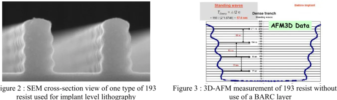
At the origin of this study, we would like to simply use the benefit of using the 3D-AFM technique in order to benchmark different resists for implant lithography process development. The goal was to study and optimize standing waves on the final resist profile and study how the profile was impacted after an implant process step. As illustrated in figure 2, after the lithography step, as there was no BARC layer we can clearly identify standing waves formation on the cross-section SEM view. After measuring it by 3D-AFM, we have validated that we were able to obtain the same level of accuracy without cleaving the wafer and therefore saving time and cost as illustrated in figure 3 that shows the 3D-AFM results on such resist profile. The tapered profile observed on figure 3 is just due to a non 1:1 scale. In this case, there was no issue with the 3D-AFM used as there was no tip wear and excellent data quality.
AFM3D Data
Figure 2 : SEM cross-section view of one type of 193 resist used for implant level lithography
Figure 3 : 3D-AFM measurement of 193 resist without the use of a BARC layer
Afterwards, we applied an implant process on the resist and look at the new resist profile with the 3D-AFM technique in order to see how this type of resist was degrade during the process and if the new profile was acceptable for the following technological steps. The results are illustrated on figure 4. On a first look, we can clearly see that standing waves amplitude does not change during the implant process from 5keV up to 20keV. However, the important point that we have to look at is represented on figure 5. Indeed, as we can clearly see on this figure, for a 40keV implant process, the tip wear level (20% diameter drop after only 5 measurements) is very important and has reached a level which is definitely not acceptable for the use of the 3D-AFM technique in a fab environment.
Based on this result, we decide to evaluate and quantify the modifications induced by implantation on resist surface. Subsequently, the final goal is to understand the reason why these new surface characteristics lead to changes in 3D-AFM tip-surface interactions.
AnaIysis Type olanalysis: Characteristics:
XPS Exeme surface
(depth 10 nm)
Surbce (depth 50 nm)
Contact ane Etheme surtace
(depth I nm)
- non dest,thve
— in - itij measurement
- chemical bindings and atomic quanhficabon - non desbuclive
- Ajnctonal groups hands of vibrations dersnination
- non desthjche
- wettabity and surtace free energy detemilnaton
Leaving Lactone Polar
Group
Group Group
—+-=o1 jJ
\1.\F\1.•%/a-GBI%IAIRA]\IA
L/S 130 nm 1:1 0 20 40 60 80 100 120 140 160 180 200 220 240 -350 -250 -150 -50 50 150 250 350 Li n e s H e ight in nmBefore implant 5 KeV 10 keV 20 KeV
0.6 0.65 0.7 0.75 0.8 0.85 0.9 0.95 1 0 1 2 3 4 5 6 Number of measurements N o rm iliz e d t ip d ia m e te r Tip diameter 20% drop 40keV
Figure 4: 3D-AFM measurements of resist profiles after an implant process for various energy levels
Figure 5: Normalized 3D-AFM flared silicon tip width variation as a function of number of measurements on resist profiles after applying a 40keV implant process
3.2. PROTOCOL OF THE ADVANCED STUDY ON TIP WEAR ORIGIN
Our reference resist for the study is a 193 resist (a Methacrylate matrix-based resist). We have compared two different implant process conditions: 1-40keV/8.5E14at/cm2
and 2-10keV/5E13at/cm2. After the
evaluation of all the modifications on surface that would be responsible for 3D-AFM tip damaging, we will correlate data from the different analysis methods and afterwards try to find a tip coating allowing reliable measurements with the 3D-AFM technique in order to implement it potentially in a production environment.
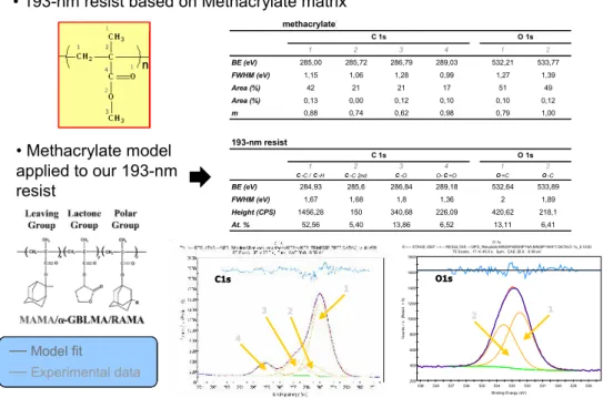
For this specific study, we decide to move from patterned wafers to blanket wafers in order to allow the chemical surface analysis with XPS, FTIR, ATR and contact angle measurements on the same wafers. The figure 6 summarizes the measurement capability of each technique. We have divided the study in 3 parts, extreme surface analysis (XPS and Contact angle), surface analysis (ATR) and volume analysis (FTIR). As a reminder, the figure 7 represents the typical chemical compositions of a 193 resist based on a methacrylate matrix. Each group that has been represented on this figure play a key role in the resist behavior related to lithography performance, the etching selectivity during plasma etching, resist adhesion on substrate (…). In our study we will identify and follow the behavior of each group.
3.3. RESULTS
3.3.1. Reference measurements
We have started to acquire reference data from each technique in order to have access to the chemical “signature” of the initial 193 resist before applying the implant process. The presented FTIR and ATR spectra are only data extracted from the full spectrum. The figure 8 and 9 show respectively the XPS and FTIR/ATR signatures of the 193 resist.
We can clearly see on figure 8, that the model choose (Methacrylate model, blue curve), for our XPS analysis fit, is in keeping with the experimental data (red curve). On the figure 9, we can clearly identify all the main groups’ constituents of our 193-nm resist.
Figure 6: Material’s chemical analysis capability of each technique
Figure 7: Typical chemical composition of a Methacrylate matrix-based 193nm resist
193-nm resist: Reference XPS
• 193-nm resist: based on PMMA matrix
1 2 4 3 C1s 1 2 4 3 C1s 1 2 4 3 C1s 200 400 600 800 1000 1200 1400 1600 1800 528 529 530 531 532 533 534 535 536 537 538 539 C oun ts / s ( R es id. × 5)
Binding Energy (eV) O 1s
E:\--- STAGE 2007 ---\--- RESULTAS ---\XPS_Résultats\M925P\M925P19A\M925P19AFT.DATA\O 1s_0.VGD 75 Scans, 17 m 45.0 s, 0µm, CAE 20.0, 0.09 eV 1 2 O1s 200 400 600 800 1000 1200 1400 1600 1800 528 529 530 531 532 533 534 535 536 537 538 539 C oun ts / s ( R es id. × 5)
Binding Energy (eV) O 1s
E:\--- STAGE 2007 ---\--- RESULTAS ---\XPS_Résultats\M925P\M925P19A\M925P19AFT.DATA\O 1s_0.VGD 75 Scans, 17 m 45.0 s, 0µm, CAE 20.0, 0.09 eV 1 2 O1s 1 2 O1s 1 2 3 4 1 2 BE (eV) 285,00 285,72 286,79 289,03 532,21 533,77 FWHM (eV) 1,15 1,06 1,28 0,99 1,27 1,39 Area (%) 42 21 21 17 51 49 Area (%) 0,13 0,00 0,12 0,10 0,10 0,12 m 0,88 0,74 0,62 0,98 0,79 1,00 C 1s O 1s
Poly(methyl methacrylate) (PMMA)
1 2 3 4 1 2 C -C / C -H C -C 2nd C -O O-C =O O =C O -C BE (eV) 284,93 285,6 286,84 289,18 532,64 533,89 FWHM (eV) 1,67 1,68 1,8 1,36 2 1,89 Height (CPS) 1456,28 150 340,68 226,09 420,62 218,1 At. % 52,56 5,40 13,86 6,52 13,11 6,41 C 1s O 1s 193-nm resist
• PMMA model applied
to our 193-nm resist
¨
n 1 2 3 4 2 1 1 n 1 2 3 4 2 1 1 n 1 2 3 4 2 1 1 n 1 2 3 4 2 1 1 O C H2 20 C C O O C H2 C C O O CH2 40 C CH3 O 40 CH3 C H3 O H O O O C H2 20 C C O O C H2 C C O O CH2 40 C CH3 O 40 CH3 C H3 O H O O¨
—Model fit —Experimental data —Model fit —Experimental data• 193-nm resist based on Methacrylate matrix
• Methacrylate model applied to our 193-nm resist
Figure 8: XPS reference data on our 193-nm resist before the implant process
193-nm resist: Reference FTIR and ATR
2700 2800 2900 3000 3100 3200 3300 3400 3500 3600 3700 3800 -0,001 0,000 0,001 0,002 0,003 0,004 0,005 0,006 0,007 0,008 A bs or banc e Wavenumber [cm-1] Reference 2700 2800 2900 3000 3100 3200 3300 3400 3500 3600 3700 3800 -0,005 0,000 0,005 0,010 0,015 0,020 0,025 A b s o rbanc e Wavenumber [cm-1] Reference FTIR
¨
FTIR¨
ATR¨
ATR¨
1500 1550 1600 1650 1700 1750 1800 1850 1900 0,000 0,005 0,010 0,015 0,020 A bs or banc e Wavenumber [cm-1] Reference (1) (3) (2) (5) (4) (4) Abso rb an c e A b so rb an ce Wavenumber [cm-1] Wavenumber [cm-1] 1500 1550 1600 1650 1700 1750 1800 1850 1900 0,000 0,005 0,010 0,015 0,020 A bs or banc e Wavenumber [cm-1] Reference (1) (3) (2) (5) (4) (4) Abso rb an c e A b so rb an ce Wavenumber [cm-1] Wavenumber [cm-1] —Reference —Reference (1) (3) (2) (5) (4) (4) 1500 1550 1600 1650 1700 1750 1800 1850 1900 -0,005 0,000 0,005 0,010 0,015 0,020 0,025 0,030 A bs or banc e Wavenumber [cm-1] Reference Wavenumber [cm-1] Ab s o rb an ce Ab s o rb an ce Wavenumber [cm-1] (1) (3) (2) (5) (4) (4) 1500 1550 1600 1650 1700 1750 1800 1850 1900 -0,005 0,000 0,005 0,010 0,015 0,020 0,025 0,030 A bs or banc e Wavenumber [cm-1] Reference Wavenumber [cm-1] Ab s o rb an ce Ab s o rb an ce Wavenumber [cm-1] CH3 CH2 C CH3 CH2 C CH3 CH2 C O C = O C = O C = O O OH O m n q (4) (5) (3) (2) (3) (1) O = O CH3 CH2 C CH3 CH2 C CH3 CH2 C O C = O C = O C = O O OH O m n q (4) (5) (3) (2) (3) (1) O = O 5 1 2 4 301 a) N
0
=
to=
=
0
0
1—Reference Implant 1 = 4OkeVBinding energy [eV]
] — = ] — — — —
Imp/ant: 4OkeVvs. IOkeV- Contact angle
Reference Implant I = 4OkeV
® Implant2 = lOkeV • Polar part • Disperse part
3.3.2. Measurements after implant processes at 10keV and 40keV
XPS
The figure 10 shows the O1s peak after XPS analysis. The Reference and the two implant conditions are compared on this figure. The Implant 1 condition induces a soft shift to lower binding energy. It seems that eventually other
type of O bonding (i.e H2O or OH) has appeared.
However the implant 2 has no impact on the O1s bindings.
FTIR and ATR
The figure 11 shows the results obtained with FTIR and ATR techniques and compares the reference to the two implant conditions. The thing that is very important in our case to focus on is the H2O/-OH peak that appears on both FTIR and ATR results. It confirms our initial hypothesis makes after the XPS results that the 193-nm resist which is initially relatively hydrophobic seems to become hydrophilic after the 40keV implant process condition because of H2O adsorption.
On the basis of this result, we have carried out some contact angle measurements in order to confirm the trend observed in the case of the two process conditions.
CONTACT ANGLE
Polymers are low compact material with low surface free energy, generally ranging from 10 to 50mN/m (assuming a repeatability of 2-3mN/m). The figure 12 shows the results coming from contact angle measurements and comparing the reference to the two implant process conditions. We can clearly see that in the case of the implant 1 condition, the surface is drastically modified as the surface free energy increases both for the dispersive and polar parts. However, the implant 2 condition does not show any increase and the polar part tends to decrease compare to the reference.
Figure 10: XPS data analysis comparing the reference and the two implant process conditions for the O1s peak
FTIR
ATR
H2O/-OH H2O/-OH
Figure 11: FTIR and ATR data analysis comparing the reference and the two implant process conditions and showing the presence of
H2O/-OH
Figure 12: Contact angle data analysis comparing the reference and the two implant process conditions
Finally we can clearly conclude that the main origin of the premature wear of flared silicon tip used in this particular case seems to be the hydrophilicity of the sample during measurements which leads to higher sticking coefficient of the tip. This idea related to the use of the 3D-AFM technique has been previously mentioned in Liu et al10 work but they do not demonstrate anything. It is the case now based on our work. In order to confirm this hypothesis, we have developed our homemade hydrophobic conformal coating. The figure 13 shows the results obtain with this hydrophobic treatment by measuring 193-nm resist after a 40keV implant process. The tip diameter evolution is compared to the first result obtain with a conventional flared silicon tip.
This conclusion and potential industrial solution open the way for multiple applications for the 3D-AFM technique in the semiconductor industry as one the main issue (the tip wear) could be solved.
4. LER/LWR TRANSFER DURING PLASMA ETCHING FOR ULTIMATE PATTERNING
As an illustration of this work, we have started to work on LER/LWR transfer during plasma etching for ultimate gate patterning. The measurement protocol for this work is presented on figure 14. It consists of using the 3D-AFM technique and its ability to track sidewall information in
order to extract LER and LWR information after each technological step involved in gate patterning. In our case, the studied material stack is quite simple and consists in 193 resist, BARC layer and Poly-Silicon layer for the final transistor gate definition.
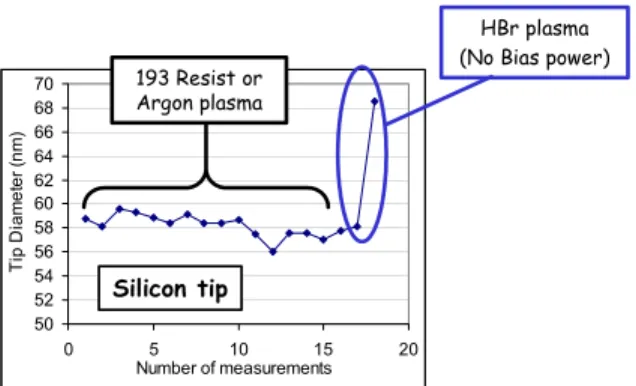
The step 1 representing the initial 193-nm resist LWR measurement is quite simple to carry out with the 3D-AFM technique. Typically, before carrying out the step 2 that consists in opening the BARC layer, we have to improve the 193-nm resist selectivity to plasma etching by applying an HBr plasma (so called: cure process) otherwise the transfer of the pattern into the final gate could be difficult for ultimate
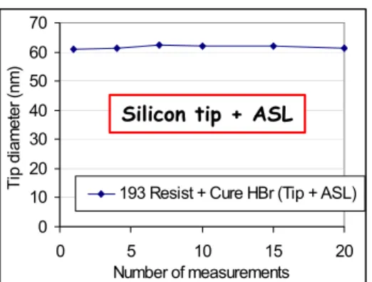
patterning. We have therefore carried out some LWR measurement after HBr plasma. The figure 15 represents the tip diameter evolution as a function of the number of measurements and related process applied for each measurement. It consists in the measurement of 193 resist first and then the same 193 resist after a cure process. We can clearly see that when applying HBr plasma we had particle contamination of our tip which subsequently makes impossible the advanced LWR study and leads to high cost per measurement. Therefore, we have applied our hydrophobic coating on our silicon tip in order to see if it could also solve the particle contamination issue. The figure 16 shows the results obtain in term of tip diameter evolution as a function of the number of measurements done on 193 resist after applying only HBr plasma.
Results after tip coating for implant process
0.6 0.65 0.7 0.75 0.8 0.85 0.9 0.95 1 0 5 10 15 20 Number of measurements N o rm il iz e d t ip di am et er
Tip without any treatment Tip with treatment
Figure 13: Tip diameter evolution with and without hydrophobic coating as a function of the number of measurements on a 193-nm resist previously exposed to
an implant process at 40keV energy.
Measured areas 2)BARC Opening 3) Gate etching HBr/Cl2/O2 4)Stripping+HF p-Si (100nm) BARC (80nm) SiO2 c-Si 1)Lithography >300nm Measured areas 2)BARC Opening 3) Gate etching HBr/Cl2/O2 4)Stripping+HF p-Si (100nm) BARC (80nm) SiO2 c-Si 1)Lithography >300nm >300nm
Figure 14: 3D-AFM protocol used to study LER/LWR transfer during silicon gate patterning
50 52 54 56 58 60 62 64 66 68 70 0 5 10 15 20 Number of measurements T ip D ia m et er ( nm ) HBr plasma (No Bias power) 193 Resist or
Argon plasma
Silicon tip
Figure 15: Tip diameter evolution as a function of the number of measurements and process conditions
Br'u2 F"m't Open C esist+ BPC O CF4 esist+b. 30 CI2fO esist+BAJ dBrfCI2fO2 esist+BP
Anti—stidc jig byir
We can clearly see that the hydrophobic coating here again has been very efficient to solve this problem of particle contamination after an HBr plasma process. Based on this result we have continued to study various plasma chemistries that are summarized on the figure 17 for which we had some trouble with particle contamination or tip premature wear. As it is illustrated in the 2nd column on figure 17, when using the tip coated (called ASL which stands for Anti-sticking layer) with hydrophobic layer, most of the plasma chemistries that used to present some issues have been solved except for two of them. We assume that another wear mechanism of the tip could be complementary to the hydrophilicity of the sample.
0 2 4 6 8 10 12 14 polySi BARC Resist Resist <L W R > (n m ) Etched poly-Si
Litho Barc Open Stripping+HF
Etching « conventional »
with Barc Open CF4
Etching with trim/ with Open HBr/O2 50s
Etching with trim/
with Open HBr/O2 70s
0 2 4 6 8 10 12 14 polySi BARC Resist Resist <L W R > (n m ) Etched poly-Si
Litho Barc Open Stripping+HF 0 2 4 6 8 10 12 14 polySi BARC Resist Resist <L W R > (n m ) Etched poly-Si
Litho Barc Open Etched Stripping+HF poly-Si
Litho Barc Open Stripping+HF
Etching « conventional »
with Barc Open CF4
Etching with trim/ with Open HBr/O2 50s
Etching with trim/
with Open HBr/O2 70s
Figure 17: Number of successful measurements as a function of plasma chemistries
Figure 18: LWR transfer from the lithography step down to the silicon gate definition. The influence of a plasma resist trimming process is presented
The figure 18 illustrates one of the final result obtains with such LWR study. This graphic represents the LWR evolution as a function of the technological step applied on a wafer in order to design a silicon gate based on the top-down approach. In addition to the successive technological step, we have compared the LWR transfer with and without a 193 resist trimming process. Such plasma process is very useful in order to make smaller devices and therefore by-pass ultimate lithography resolution that could not be currently achieved. We can clearly see on this graphic that for both processes (with and without resist trimming), the final silicon gate LWR is the same value than the one of the BARC LWR. If we now compare with and without a resist trimming process, we can clearly see that without it, the LWR reduction between the initial 193 resist and the final silicon gate is around 15% whereas with this specific resist trimming process the reduction has reached 45% and remain at this same level on the final gate.
5. ADVANCED APPLICATION FOR NEW PROMISING MULTIWIRES DEVICES FABRICATION
After exploring and extending the potential applications of the 3D-AFM technique to fundamental plasma etching studies and implant process studies, we would like to combine both complex structure measurement and validate on it
0 10 20 30 40 50 60 70 0 5 10 15 20 Number of measurements T ip d iam et er (nm )
193 Resist + Cure HBr (Tip + ASL) Silicon tip + ASL
Figure 16: Tip diameter evolution as a function of the number of measurements on 193 resist after HBr plasma process
— —
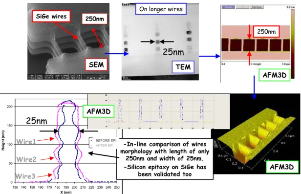
the capability of the 3D-AFM technique to reach the nanometer resolution. In order to carry out this experiment, we have processed new promising multiwires device wafer as it shown on the figure 19 on the first cross-section image. We can clearly see the three different SiGe wires with void between each. The final goal in a near future is to control the sidewall roughness of the wires, control the width and the shape in the range of 20nm and once they are fabricated, the goal is to control within few nanometers of accuracy the Si epitaxy on these SiGe wires. The useful devices have wires with a length of 250nm. Typically, in order to control the process, engineers are doing cross-section images and In-line TEM analysis on longer wires because the sample preparation is impossible on only 250nm wire length. Our goal is therefore to validate the capability of the 3D-AFM to control the overall process fabrication on real devices with a 250nm length and faster than with these two techniques in order to reduce R&D cost.
The figure 19 shows the 3D-AFM results. We have validated the capability to measure the wires with a length of 250nm. On the average 3D-AFM profile (blue curve), we can clearly identify all the wires that present a width in the range 25nm as it has been measured with TEM analysis. On the final graphic which is the superimposing of the 3D-AFM wires measurements before and after the Silicon epitaxy on the SiGe wires, we have validated the capability of the 3D-AFM technique to characterize such process at the exact same position before and after the epitaxy process which is strictly impossible with another current CD metrology technique.
SEM AFM3D 250nm AFM3D 250nm AFM3D AFM3D SiGe wires 250nm TEM
25nm
On longer wires TEM25nm
On longer wires 0 50 100 150 200 130 140 150 160 170 180 190 200 210 220 230 240 250 X (nm) H e ight ( n m ) AVANT EPIAPRES EPI -In-line comparison of wires
morphology with length of only 250nm and width of 25nm. -Silicon epitaxy on SiGe has
been validated too
25nm
Wire1 Wire2 Wire3 0 50 100 150 200 130 140 150 160 170 180 190 200 210 220 230 240 250 X (nm) H e ight ( n m ) AVANT EPIAPRES EPI -In-line comparison of wires
morphology with length of only 250nm and width of 25nm. -Silicon epitaxy on SiGe has
been validated too
25nm
Wire1 Wire2 Wire3 AFM3D AFM3D BEFORE EPI AFTER EPIFigure 19: Example of a complex multiwires device that has been characterized with the 3D-AFM technique
6. CONCLUSION
The tip wear is a strong limitation for a massive introduction of the 3D-AFM technique for advanced process control in order to be complementary to Scatterometry and CD-SEM techniques and allow fab environment to get enough CD measurement accuracy compatible with roadmap requirements.
In this study we have shown that the hydrophilicity of samples is partly responsible of tip damage due to higher sticking coefficient (particle pick-up or tip erosion) that occurs during some implant process and during plasma etching processes. We have shown that hydrophobic coating realized on conventional flared silicon tips is the only way to overcome premature tip damage. However, it is not enough as we are still not able to measure for example resist pattern that have been etched with Cl2/O2 plasma chemistry. It opens the way to understand more deeply the tip to sample interaction. In any case, by using such hydrophobic tip, it has allowed us to work in advance on LER/LWR transfer during plasma etching processes for example by showing that applying a resist trimming process could reduce the initial 193 resist LWR by a factor of 45% on the final silicon gate. When combining such a tip with recent 3D-AFM
enhancements, we have been able to fully characterize in advanced a new promising complex multiwires devices that currently no other in-line technique (either CD-SEM or Scatterometry) are able to measure.
The 3D-AFM industry has to work hard and fast on manufacturing such hydrophobic tips and continuing to improve tip servoing in order to help the semiconductor industry to reach the accuracy that is required by the ITRS and by all the other CD metrology techniques which require accurate calibration within 1nm.
ACKNOWLEDGEMENTS
The authors would like to thank the different persons involved in LETI multiwires devices fabrication (T.Ernst, V.Delaye, J-M.Hartmann, S.Pauliac, C.Vizioz). We would also like to thank A.Pikon (Rohm&Haas) for providing 193 resist, cross-section images and related AFM3D data. Finally, we would like to thank all the Veeco R&D team in Santa Barbara for fruitful discussions on the 3D-AFM technique.
REFERENCES
1
« The Atomic Force Microscope » -G.Binnig, C.F.Quate and Ch.Gerber -Phys.Rev.Lett. 1985. 2
« AFM mapping and profiling on a sub-100Å scale » -Y.Martin, H.K Wickramasinghe, Appl.Phys.Lett. 1987. 3
« Method for imaging sidewalls by AFM » -Y.Martin, H.K Wickramasinghe, Appl. Phys. Lett. 1994. 4
« Tip Characterization and surface reconstruction of complex structures with CD-AFM » -G.Dahlen et al, J. Vac. Sci. Technol.B, 2005.
5
« TEM validation of CD-AFM image reconstruction » -G.Dahlen et al, Proc.SPIE Microlithography, 2007 6
« Advances in CD-AFM scan algorithm technology enable improved CD Metrology » -L.Mininni, J.Foucher, Proc. SPIE Microlithography, 2007.
7
« Study of 3D metrology techniques as an alternative to cross-sectional analysis at the R&D level» J.Foucher and K.Miller, Proc. SPIE53 75, 444 (2004).
8
« From CD to 3D Sidewall Roughness Analysis with 3D CD-AFM», J.Foucher, Proc. SPIE 5752, 966 (2005). 9
« Minimizing CD Measurement Bias through Realtime Acquisition of 3D Feature Shapes» J.Foucher, D.Gorelikov, M.Poulingue, P.Fabre, and G.Sundaram,Proc. SPIE 6152, 61521A (2006).
10