Chemical Approaches to Organometallic Chemical
Vapor Deposition of Wide Band-Gap II-VI Layers
and Nanocrystal Composites
by
Michal Danek
B.S. Inorganic Chemistry, Charles University, Prague (1987) M.S. Inorganic Chemistry, Charles University, Prague (1987) Submitted to the Department of Chemistry in Partial Fulfillment of the
Requirements for the Degree of
Doctor of Philosophy
at the
Massachusetts Institute of Technology
February 1995© 1995 Massachusetts Institute of Technology All rights reserved
Signature of Author
Department 0, emistry -•4,',•fary 17, 1995 Certified by
Klavs F. Jensen Professor, Department of Chemical Engineeri g and Materials Science Thesis Supervisor Accepted by
Dietmhr Seyferth Professor of Chemistry Chair, Departmental Committee on Graduate Students
This doctoral thesis has been examined by a Committee of the Department of Chemistry as follows:
Professo Moungi G. Bawendi, Chairman
Professor Kla .
Jensen,
Thesis AdvisorChemical Approaches to Organometallic Chemical Vapor
Deposition of Wide Band-Gap II-VI Layers and Nanocrystal
Composites
byMichal Danek
Submitted to the Department of Chemistry on January 17,1995 in partial fulfillment of the requirements for the degree of
Doctor of Philosophy in Inorganic Chemistry
Abstract
Organometallic chemical vapor deposition (OMCVD) of ZnTe was explored with tert-butyl(trifluoromethyl)tellurium, a novel precursor with a high vapor pressure and low decomposition temperature. Contamination of ZnTe films with ZnF2 crystallites was observed at growth temperatures below 400 'C, while almost pure ZnTe films were grown above 400 'C. Growth from bis(trifluoromethyl)tellurium yielded ZnTe films with low fluorine concentrations. The contamination mechanism was probed by molecular beam mass spectroscopy under OMCVD growth conditions.
OMCVD of epitaxial ZnSe was explored with new organometallic selenium precursors. Particular emphasis was placed on the development of precursor chemistry for low temperature growth and p-type doping of ZnSe. Growth experiments with tert-butyl(allyl)selenium, in combination with (CH3)2ZnN(C2H5)3, yielded films with good surface morphologies and negligible carbon contamination (<5x101 7 atoms/cm3). Low temperature photoluminescence spectroscopy and double crystal x-ray diffraction were used to assess the crystallinity and optical quality of the layers. Gas-phase pyrolysis of
tert-butyl(allyl)selenium was investigated by molecular beam mass spectrometry
and a pyrolysis mechanism of the precursor under OMCVD conditions was proposed. Tripropylphosphine selenide, in combination with dimethylzinc and a helium carrier gas, allowed growth of epitaxial ZnSe at 375-450 TC. The films possessed good photoluminescence spectra and smooth surface morphologies. Secondary ion mass spectrometry (SIMS) confirmed negligible carbon and phosphorus incorporation (<2x101 7 atoms/cm3 and <1017 atoms/cm3, respectively). The hydrogen content in the layers was low, comparable to the detection limit of SIMS (~1018 atoms /cm 3). The possibility to increase the volatility of phosphine selenide precursors was explored with dimethyl(alkyl)phosphine selenides. Growth experiments with
dimethyl(butyl)phosphine selenide yielded ZnSe films of high quality, comparable to the layers synthesized from tripropylphosphine selenide.
Novel CdSe/ZnSe quantum dot composites for light emitting devices were synthesized by a new technique combining electrospray and OMCVD. In this technique, size selected CdSe nanocrystals are transferred into an OMCVD reactor by electrospray and co-deposited with a ZnSe matrix synthesized from hydrogen selenide and diethylzinc. The microstructure of the composites was probed by high resolution transmission electron microscopy, scanning transmission electron microscopy, Auger electron spectroscopy and x-ray diffraction. The composite films showed room temperature photoluminescence characteristic of the incorporated nanocrystals.
To enhance luminescence properties of CdSe/ZnSe composites, the surface of CdSe nanocrystals was electronically passivated by an overlayer of ZnSe. The ZnSe overlayer was synthesized prior to the electrospray OMCVD synthesis via an organometallic solution route. CdSe/ZnSe particles were characterized by high resolution electron transmission microscopy, optical absorption and photoluminescence spectroscopies, x-ray fluorescence, Auger electron spectroscopy analysis, and x-ray diffraction. A dramatic enhancement of photoluminescence yield (by two orders of magnitude) and improved thermal stability of the composites were obtained with the passivated nanocrystals.
Thesis Supervisor : Professor Klavs F. Jensen
Contents
List of figures 7
List of schemes and tables 15
1. Introduction 16
1.1. The scope of the thesis and research goals 20
1.2. Literature review 21
1.2.1. OMCVD of Wide Band Gap II-VI Semiconductors 21 1.2.2. OMCVD Precursors for ZnSe and ZnTe 23 1.2.3. Semiconductor Quantum Dot Composites 28 1.2.4. Electronic passivation of Quantum Dots with a
Wide Band Gap Overlayer 30
1.3. Thesis Outline 32
2. tert-Butyl(trifluoromethyl)tellurium - a novel OMCVD
source for ZnTe 39
2.1. Introduction 39
2.2. Experimental 41
2.3. Results and discussion 45
2.3.1. Growth and materials characterization 45 2.3.2. Gas-phase pyrolysis study of tBTeCF3 53
2.4. Conclusion 62
3. OMCVD growth and pyrolysis study with
tert-butyl(allyl)selenium 64
3.1. Introduction 64
3.2. Experimental 65
3.3. Results and discussion 69
3.3.1. Growth and characterization of ZnSe 69 3.3.2. Gas-phase pyrolysis study of tBASe 75
4. OMCVD of ZnSe with tripropylphosphine selenides 97
4.1. Introduction 97
4.2. Experimental 100
4.3. Results and discussion 102
4.3.1. OMCVD with tripropylphosphine selenide
(TPPSe) 102
4.3.2. OMCVD with dimethyl(butyl)phosphine selenide
(DMBPSe) 116
4.4. Conclusion 123
5. Electrospray OMCVD synthesis of CdSe/ZnSe quantum dot
composites 127
5.1. Introduction 127
5.2. Experimental 128
5.3. Results and discussion 132
5.4. Conclusion 146
6. Synthesis and Characterization of CdSe/ZnSe Composites
with Passivated CdSe Nanocrystals 149
6.1. Introduction 149
6.2. Experimental 150
6.3 Results and discussion
6.3.1. Synthesis and characterization of CdSe/ZnSe
nanoparticles 154
6.3.2. Synthesis of CdSe/ZnSe composites with
passivated nanocrystals 165
6.4. Conclusion 177
7. Conclusions and Future Work 180
Acknowledgments 183
List of Figures
Figure 1.1 Figure 1.2 Figure 2.1. Figure 2.2. Figure 2.3. Figure 2.4. Figure 2.5. Figure 2.6. Figure 2.7. Figure 2.8. Figure 2.9. Figure 2.10.A schematic of a full color thin film electroluminescent display (TFED) [3] and cold cathode field emission display
(FED) [2a].
A schematic of a blue LD [8].
Schematic of the microbalance system.
Schematic of the molecular beam mass spectrometer (MBMS) system.
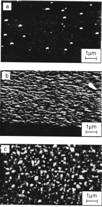
SEM micrographs of films grown from tBTeCF3 at various substrate temperatures at [Te/Zn] = 1.0. (a) 4000C, (b) 3500C
and (c) 3000C.
SEM micrographs of films grown from tBTeCF3 at various [Te/Zn] ratios at 3500C. (a) 2.5 and (b) 0.25.
Auger electron spectra of films grown at [Te/Zn]=1.0. (a) film from tBTeCF3 at 4000C (surface sputtered), (b) film with crystallites from tBTeCF3 at 3500C, (c) crystallite on film from tBTeCF3 at 3000C, (d) film between crystallites from tBTeCF3 at 3000C, and (e) film from (CF
3)2Te at 5000C (surface sputtered).
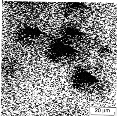
SIMS fluorine map of a film grown from tBTeCF3 at 4000C. Black color indicates an elevated fluorine content.
X-ray diffraction of films grown at [Te/Zn] =1.0. (a) film from tBTeCF3 at 4000C, (b) film from tBTeCF3 at 3500C, (c) film from tBTeCF3 at 3000C, (d) film from (CF3)2Te at 5000C.
Arrhenius plot for growth from tBTeCF3 at [Te/Zn] equals to 2.0 (1), 1.0 (n) and 0.5 (s). The flux of tBTeCF3 was varied.
Growth rate of ZnTe at 4400C at various [Te/Zn] ratios. The flux of tBTeCF3 was varied.
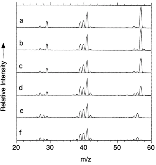
MBMS spectra of tBTeCF3 pyrolysed in hydrogen at 4120C (a), in helium at 3980C (b). The peak denoted by (*) corresponds
18 19 42 44 46 47 48 49 51 52 54
Figure 2.11. Figure 2.12. Figure 2.13. Figure 3.1. Figure 3.2. Figure 3.3. Figure 3.4. Figure 3.5.
to SiF3+. It is observed only above the decomposition temperature of the source and may have its origin in the reaction of HF with the quartz insulating plate of the MBMS heater.
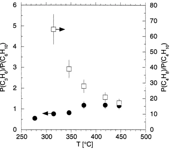
Normalized MBMS intensities of the gas-phase species for pyrolysis of tBTeCF3 in H2 at 30 Torr. The following symbols are used: A parent, Q methylpropene (m/z=56), 0 2-methylpropane (m/z=43), * hydrogen fluoride (m/z=20), A tetrafluoroethene (m/z=100), M 1,1-difluoro-2,2-dimethyl-cyclopropane (m/z=91).
Effect of 2-methylpropene addition on the ratio of ion signals at m/z=100 (tetrafluoroethene) and m/z=91 (1,1-difluoro-2,2-dimethylcyclopropane) during pyrolysis of tBTeCF3. (a) tBTeCF3 (20 gmol/min) in hydrogen, (b) tBTeCF3 (20 gmol/min) and 2-methylpropene (170 gmol/min) in hydrogen.
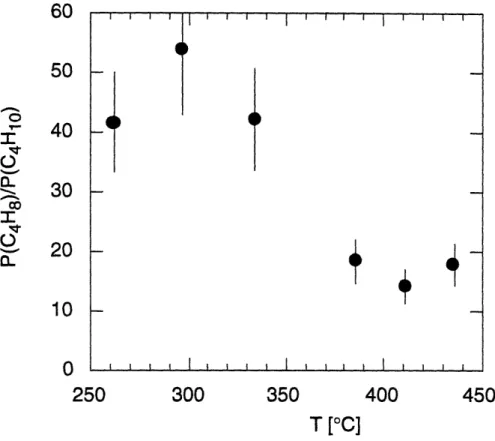
Ratio of 2-methylpropene vs. 2-methylpropane pressures as a function of heater temperatures pyrolysis of tBTeCF3.
partial during
Schematic of the OMCVD reactor.
Growth rate of ZnSe for MASe (m), DASe (*) and tBASe (0) as a function of substrates temperatures. The growth rate data for DASe and MASe are from ref. [4].
SEM images of the surface morphology of ZnSe films deposited from tBASe (40gimol/min) and DMZnNEt3 (20jimol/min) in hydrogen at various growth temperatures: (a) 325*C (b) 350°C (c) 400°C.
Low temperature (10 K) photoluminescence spectra of ZnSe grown from tBASe (40 pmol/min) and DMZnNEt3
(20gmol/min) in hydrogen at 3500C.
Dependence of carbon concentration on the [VI/II] ratio for ZnSe films grown from MASe (m) [growth at 520 °C], DASe
(*)
[growth at 400 'C] and tBASe (0) [growth at 3500C]. The samples from MASe and DASe were prepared previously [4].57 60 61 67 70 71 73 74
Figure 3.6. Figure 3.7. Figure 3.8. Figure 3.9. Figure 3.10. Figure 3.11. Figure 3.12. Figure 3.13. Figure 3.14.
Molecular beam mass spectra of the gas-phase recorded during pyrolysis of tBASe in hydrogen at 100 OC (a), 240 OC
(b), and 440 'C (c). The spectra are corrected for the temperature dependence of the sampling flux.
Partial pressures of tBASe and the hydrocarbon products in the gas-phase during pyrolysis of tBASe in hydrogen at various temperatures; * tBASe, 0 propene, O 2-methyl-propene, A 2-methylpropane, and O 1,5-hexadiene.
Partial pressure ratios of propene vs. 1,5-hexadiene (0) and 2-methylpropene vs. 2-methylpropane (U) for the pyrolysis of tBASe in hydrogen.
Relative MBMS intensities of tBASe and DASe for pyrolysis of tBASe in hydrogen. 0 tBASe (m/z=178 amu) and 0 DASe
(m/z=162 amu).
The hydrocarbon region of the molecular beam mass spectra recorded during pyrolysis of tBASe in deuterium and hydrogen: (a) 100 TC in deuterium, (b) 100 TC in hydrogen, (c) 2500C in deuterium, (d) 240 oC in hydrogen, (e) at 450 'C in
deuterium, and (f) 440 'C in hydrogen.
Molecular beam mass spectra of the gas-phase for co-pyrolysis of an equimolar mixture of tBASe and DMZn in hydrogen at 100 TC (a), 3200C (b), and 450 TC (c). The spectra are corrected
for the temperature dependence of the sampling flux.
Partial pressures of tBASe, DMZn and the hydrocarbon products for co-pyrolysis of tBASe and DMZn in hydrogen at various temperatures; 0 tBASe, X DMZn,
*
methane , A ethane, N propene, U 2-methylpropene, A 2-methylpropane, and O 1,5-hexadiene.The partial pressure ratios of propene vs. 1,5-hexadiene (0)
and 2-methylpropene vs. 2-methylpropane (Q) for co-pyrolysis of tBASe and DMZn in hydrogen.
Relative MBMS intensities of tBASe, DASe, MASe and DMSe for pyrolysis of tBASe in hydrogen at various temperatures; * tBASe (m/z=178 amu), 0 DASe (m/z=162 amu), + MASe (m/z=136), and V DMSe (m/z=110 amu).
76 77 79 80 81 87 88 90 91
Figure 4.1.
Figure 4.2.
Schematic of the OMCVD reactor and gas-handling system used for growth experiments with the phosphine selenides. 101 Temperature dependence
film was deposited from (5gmol/min) in helium at
of ZnSe growth rate. The ZnSe TPPSe (5gmol/min) and DMZn
300Torr. 103
Figure 4.3.
Figure 4.4.
Figure 4.5.
SEM images of surface morphology of ZnSe films grown from TPPSe (5tmol/min) and DMZn (5gmol/min) in He at 375 'C (a), 400 °C (b), 425 'C (c), and 450 'C (d). The layer thicknesses were -0.5gm (a,b) and ~1.0gm (c,d). 105 SIMS concentration profiles for hydrogen (a), phosphorus (b), and carbon (c) in films grown from TPPSe (5gmol/min) and DMZn (5gmol/min) in He at 400 OC (solid curve), and tBASe (40gmol/min) and DMZnNEt3 (20gmol/min) in H2 at 350 °C
(dashed curve). 106
SEM image of a ZnSe film grown from TPPSe (5gmol/min) and DMZn (5gmol/min) in H2 at 400 OC. The layer thickness was -0.5p~m. The white particles were identified by Auger
electron spectroscopy as ZnSe. 108
Figure 4.6. SIMS concentration carbon in a films DMZn (5gmol/min)
profiles for hydrogen, phosphorus, grown from TPPSe (5gmol/min) in H2 at 425 TC.
Figure 4.7.
Figure 4.8.
10 K PL spectra of ZnSe grown from TPPSe (5gmol/min) and DMZn in He at 425 'C at the [VI/II] ratio equals to 0.5 (a), 1 (b) and 2 (c). The film thicknesses were -1 pgm. 110 1.9 K near band-edge PL of ZnSe. The films were grown from TPPSe (5gmol/min) and DMZn in He at 425 'C at the [VI/II] ratio equals to 0.5 (a), 1 (b) and 2 (c). The film thicknesses
were -1 pm. 111
Figure 4.9. 10 K PL spectra of ZnSe grown from andDMZn (5gmol/min) in He at temperatures: 375 'C (a), 400 'C (b), 4250C
TPPSe (5gmol/min) various substrate (c), and 450 'C (d). 114 Figure 4.10. 1.9 K near band-edge PL of ZnSe. The films were grown from
TPPSe (5gmol/min) andDMZn (5tmol/min) in He at and and
various substrate temperatures: 375 'C (a), 400 'C (b), 4250C (c), and 450 TC (d). 115 Figure 4.11. Figure 4.12. Figure 4.13. Figure 4.14. Figure 4.15. Figure 5.1. Figure 5.2. Figure 5.3. Figure 5.4. Figure 5.5.
10 K PL spectrum of a ZnSe film grown from TPPSe (5gmol/min) and DMZn (5gtmol/min) in H2 at 400 'C. The inset shows the band-edge emission.
Vapor pressure for DMBPSe (0) and TPPSe (U) at various
temperatures.
1
SEM image of a ZnSe film grown from DMBPSe (5ýxmol/min) and DMZn (5pmol/min) in He at 425 'C. The
layer thickness was -1pm. 1
SIMS concentration profiles for hydrogen, phosphorus, and carbon in a films grown from DMBPSe (5pmol/min) and DMZn (5pmol/min) in He at 425 'C.
10 K PL spectrum of a ZnSe film grown from DMBPSe (5gmol/min) and DMZn (5pmol/min) in He at 425 'C. The layer thickness was 0.5 gim. The insert shows the band-edge emission.
Schematic of the Electrospray OMCVD reactor.
X-ray diffraction patterns of CdSe/ZnSe composites deposited by ES-OMCVD at 150 'C (a), 200 'C (b), and 250 'C (c). The size of the CdSe nanocrystals was -5.0 nm. The zinc blende and wurtzite diffractions of ZnSe are labeled with
*
and 0, respectively.SEM images of CdSe/ZnSe composites deposited by ES-OMCVD at 150 °C (a), 200 'C (b), and 250 'C (c).
AES depth profiles of Zn (n) and Cd (m) concentrations in a CdSe/ZnSe composite with -3.5 nm CdSe nanocrystals. The film was deposited at 2400C.
Optical absorption (dashed line) and PL (solid line) spectra of a CdSe/ZnSe composite incorporating -3.5 nm CdSe nanocrystals. The excitation wavelength for the PL spectrum was 470 nm. L17 L18 L19 L20 122 130 134 135 136 138
Figure 5.6. Figure 5.7. Figure 5.8. Figure 5.9. Figure 5.10. Figure 6.1. Figure 6.2. Figure 6.3.
Room temperature PL (a,b) and PL excitation (c,d) spectra of CdSe/ZnSe quantum dot composites with -3.5 nm nanocrystals (a,c) and -5.0 nm nanocrystals (b,d), respectively. The films were deposited at 1500C. The excitation wavelength for the PL spectra was 470 nm. The detection wavelengths for the PL excitation spectra were 570 nm (c) and 616 nm (d),
respectively. 139
Room temperature PL of CdSe/ZnSe quantum composites deposited at various substrate temperatures. size of the imbedded nanocrystals was -5.0 nm. excitation wavelength was 470 nm.
dot The The
141 Bright field TEM images of a CdSe/ZnSe quantum dot composite film with - 5.0 nm nanocrystals deposited on a C/Ni TEM grid at 2500C. The view shows individual CdSe
nanocrystals surrounded by grains of a ZnSe matrix. The (002) wurtzite planes of the nanocrystals are resolved
(d00 2=0.35 nm). 142
STEM image of a CdSe/ZnSe quantum dot composite film with -5.0 nm nanocrystals deposited on a C/Ni TEM grid at 2500C (a), and the corresponding Zn, Se and Cd elemental
maps (white color represents regions of high concentration levels, black color shows areas with low concentrations). 144 HRTEM image of an agglomerate of ~5.0 nm CdSe nanocrystals formed in electrospray. The agglomerate was
collected on a C/Ni TEM. 145
Evolution of the UV/Vis absorption spectra of the reaction mixture during overgrowth of -4.0 nm CdSe nanocrystals with ZnSe. The inset shows the corresponding particle sizes
as determined with HRTEM. 155
Low magnification TEM image of CdSe/ZnSe particles with [ZnSe/CdSe]=2.5. The initial size of the CdSe nanocrystals
was -4.0 nm. 157
HRTEM image of CdSe/ZnSe particles with [ZnSe/CdSe]=2.5. The initial size of the CdSe nanocrystals was -4.0 nm. 159
Figure 6.4. Figure 6.5. Figure 6.6. Figure 6.7. Figure 6.8. Figure 6.9. Figure 6.10.
X-ray diffraction spectra of -6.8 nm CdSe/ZnSe particles (a), -4.0 nm CdSe nanocrystals (b), and powder diffraction lines of wurtzite ZnSe (c) and wurtzite CdSe (d). The [ZnSe/CdSe] ratio for the overcoated particles was -2.5. 160 Optical absorption spectra of a film of CdSe/ZnSe particles with [ZnSe/CdSe]=2.5 before (a) and after (b) annealing in hydrogen at -450 "C. The calculated band-gap energy for
Zn0.7Cd0.3Se bulk is shown. 161
Optical absorption and PL spectra of CdSe (a) and CdSe/ZnSe particles with various [ZnSe/CdSe] ratios: 3.6 (b), 4.3 (c) and 4.8 (d). The samples were dispersed in pyridine. The excitation wavelength for the PL was 480 nm. 163 PL excitation spectra of CdSe (9) and CdSe/ZnSe particles with [ZnSe/CdSe] ratio of 3.6 (*), 4.3 (A) and 4.8 (U). The samples were dispersed in pyridine. The PL was detected at 570 nm and the spectra were normalized to the PL intensity at
550 nm. 166
300K PL spectra of CdSe/ZnSe composite films with bare CdSe nanocrystals (-3.5 nm). The films were synthesized by ES-OMCVD at substrate temperatures of 150 "C (a), 200 "C (b) and 250 "C (c). The excitation wavelength was 480 nm. 167 10K PL spectra of CdSe/ZnSe composite films with bare CdSe nanocrystals (~3.5 nm). The films were synthesized by ES-OMCVD at substrate temperatures of 150 "C (a), 200 "C (b) and 250 "C (c). The excitation wavelength was 480 nm. 169 300 K and 10K PL excitation spectra of CdSe/ZnSe composite films with bare CdSe nanocrystals (-3.5nm) synthesized by ES-OMCVD at 200 "C. The 300 K PL was detected at 554 nm (@), the 10 K PL detection wavelengths were 546 nm (U) and 710 nm (0). The band-gap energies of zinc blende ZnSe at 300
K and 10K are shown with the arrows. 170
Figure 6.11. 300 K PL overcoated dots was synthesized
spectra of CdSe/ZnSe composite films with CdSe nanocrystals. The size of the initial CdSe -3.7nm; [ZnSe/CdSe]=4.0. The films were by ES-OMCVD at substrate temperatures of 150 "C
(a), 200 'C (b) and 270 'C (c). The excitation wavelength was
480 nm. 172
Figure 6.12.
Figure 6.13.
Figure 6.14.
10 K PL spectra of CdSe/ZnSe composite films overcoated CdSe nanocrystals. The size of the initial dots was ~3.7nm; [ZnSe/CdSe]=4.0. The films synthesized at substrate temperatures of 150 'C (a), 200 and 270 'C (c). The excitation wavelength was 480 nm.
with CdSe were oC (b)
300 K and 10K PL excitation spectra of a CdSe/ZnSe composite film with overcoated CdSe nanocrystals. The film was synthesized by ES-OMCVD at 200 OC. The size of the initial CdSe dots was -3.7nm; [ZnSe/CdSe]=4.0. The 300 K PL was detected at 576 nm (0), the 10 K PL was monitored at 570 nm (J). The band-gaps of zinc blende ZnSe at 300 K and 10K are shown with the arrows.
Relative band-edge PL yields for CdSe/ZnSe composite films with bare and passivated CdSe dots. The samples were synthesized by ES-OMCVD at substrate temperatures of 2000C
(@) and 260 'C (U). The number of ZnSe monolayers in the passivating layer was estimated from the know size of the initial CdSe nanocrystals and [ZnSe/CdSe] stoichiometry of the composite particles assuming a symmetrical core-shell structure. The excitation wavelength was 500 nm.
173
[74
List of Schemes and Tables
Scheme 2.1. Proposed gas-phase decomposition mechanism of tBTeCF3. Scheme 3.1.
Scheme 3.2.
Table 1.1. Table 2.1.
Pyrolysis mechanism of tBASe under reduced pressure OMCVD conditions. The major low temperature reactions are shown with bold arrows. The symbol [H*] represents hydrogen radical donors.
Mechanism of formation of the selenium containing by-products for co-pyrolysis of tBASe and DMZn. The major low temperature reactions are shown with bold arrows. The symbols [H*] and [CH3*] stand for hydrogen radical and methyl radical donors; [Zn] represents zinc bearing species, such as (CH3)2Zn, CHaZn*, and elemental zinc.
Fundamental properties of wide band gap semiconductors [1] 16 Vapor oressure of tellurium OMCVD sources at 20 -- r r OC.
1. Introduction
Wide band gap II-VI semiconductors, including the binary compounds ZnS, ZnSe, ZnTe, CdS and CdSe, and their alloys, are materials with zinc blende (ZB) or wurtzite (W) structure and a large direct band gap [1]. The band gap energies of the most stable binary phases and corresponding lattice parameters and effective masses are listed in Tab. 1.1. The band gap energies for the alloys follow in many cases a linear dependence on the composition
(e.g., ZnSxSel-x or ZnxCdl-xSe), while a highly non-linear relationship is observed for other systems (e.g., ZnSxTel-x) [1]. The bonding in wide band gap II-VI semiconductors has a high degree of ionic character and the fundamental electronic properties of the materials, therefore, differ significantly from those for Si, Ge and III-V semiconductors.
Table 1.1. Fundamental properties of wide band gap semiconductors [1]
Compound Eg [eV] aZB
Inm]
aw [nml Cw [nm]1rn/mo
/moo
ZnS 3.70 5.4102 - - 0.28 [2] 0.49 [2]
ZnSe 2.70 5.6676 - - 0.16 0.75
ZnTe 2.35 6.1037 - - 0.11 0.6
CdS 2.49 - 4.1367 6.7161 0.17 0.7 (Ic)
CdSe 1.75 - 4.2999 7.0109 0.11 0.45 (Ic)
Wide band gap II-VI semiconductors are attractive materials for optoelectronics, specifically for light emitting devices. Traditionally, polycrystalline ZnS or ZnxCdl-xS doped with Mn, Cu, Ag, Cl and rare earth elements are used as efficient phosphors in cathode ray tubes (CRTs) and high field electroluminescent devices (EDs) [2]. The conventional II-VI phosphors may also become important in full color flat panel displays. Examples of promising display technologies utilizing phosphor are thin film electroluminescence displays (TFEDs) and cold cathode field emission
displays (FEDs) (Fig. 1.1) [3]. However, further improvements in the luminance and stability of phosphor materials are necessary to realize the potential of these technologies. A new approach to high luminance phosphors relies on layered structures incorporating thin films of doped materials, e.g., ZnS:Mn or ZnS:Tm, between undoped layers, e.g., ZnS or SrS [4]. The undoped films function as electron acceleration or carrier confinement layers, while the doped films emit light. One of the future prospects is construction of quantum well and superlattice phosphor structures [4]. Development of high luminance blue phosphors for both TFEDs and FEDs remains one of the most challenging problems in the field
and new combinations of host lattices and dopants are being explored [3]. Light emitting carrier injection devices, e.g., light emitting diodes (LEDs) and laser diodes (LDs), operating in the blue-green spectral region represent another important area for application of wide band gap II-VI semiconductors [5]. These devices are demanded in many areas of technology, including optical telecommunication, optical data recording, printing, displays and sensors. Epitaxial films of ZnSe and its alloys, such as ZnSxSel-x, ZnxCdl-xSe and ZnxMgl-xSySel-y, are the most promising materials for construction of II-VI LEDs and LDs because of the large band gap energies and close lattice match with GaAs substrates [6]. Construction of these devices demands growth of epitaxial layers with precisely controlled thickness and stoichiometry. Layers with a low density of structural defects, such as misfit dislocations, are required for low threshold operation and stability of the devices [7]. Such materials can be obtained by growing perfectly lattice matched alloys or strained quantum wells accommodating the lattice mismatch without defect formation. A schematic of the state of the art LD structure is shown in Fig. 1.2 to illustrate the materials complexity of the current II-VI injection devices. Such complexity imposes strict requirements on the growth and doping process [8]. In principle, II-VI semiconductors other than ZnSe can be also used for realization of injection devices. For example, the combination of ZnS (naturally n-type) and ZnTe (naturally p-type) allowed construction of blue LEDs operating at room temperature [9]. However, difficulties in finding a good substrate material makes these alternatives less practical.
Al electro Insulator Phosphol Insulator ITO elect f * 1 -~lass
-Light output
Figure 1.la. A schematic of a full color TFED [3]. The display consists of a matrix of row and column of electrodes and a stack of insulator layers and patterned phosphors emitting red, green and blue light. The luminescence is generated by a pulse of a high electric field and matrix addressing is used to excite individual pixels. The display is viewed through the glass substrate.
Light output
Figure 1.1b. A schematic of a full color FED [2a]. The electrons emitted from the microtips excite the patterned phosphors.
Pd/Pt/Au electrode Insulator
p-ZnTe contact
p-ZnSe/p-ZnTe quantum wells p-ZnSSe
p-ZnMgSSe cladding layer ZnSSe guiding layer ZnCdSe quantum well n-ZnSSe guidinglLayer n-ZnMgSSe cladding layer n-ZnSSe buffer layer n-GaAs substrate In electrode
Figure 1.2. A schematic of a blue LD [8]. The LD structure was grown on (100) n-GaAs substrate by molecular beam epitaxy (MBE). The p-n junction is formed by p-ZnSSe layer, ZnCdSe quantum well (5 nm thick) and n-ZnSSe layer. The Cd content in the ZnCdSe alloy was sufficiently high to keep the injected carriers confined in the quantum well even at room temperature. The doped ZnSSe layers surrounded by ZnMgSSe cladding layers form the laser waveguide. In order to provide for a low resistance ohmic contact to the p-type side of the device, a graded p-ZnTe/p-ZnSe quantum well structure is grown on the p-type cladding layer. The laser cavity is defined by cleaved facets covered with high reflectivity coatings. Because of low density of structural defects, the LD emits blue light in both continuous wave (CW) and pulse modes at room temperature.
1.1. The Scope of the Thesis and Research Goals
The purpose of the thesis research is to contribute to the development of organometallic chemical vapor deposition (OMCVD) of wide band gap II-VI semiconductors, specifically ZnSe and ZnTe. The emphasis is placed on the following areas:
(1) OMCVD of ZnTe with novel (trifluoromethyl)tellurium precursors. These precursors, e.g.
tert-butyl(trifluoromethyl)-tellurium (tBCF3), were recently proposed as an alternative to the low vapor pressure dialkyltellurium sources currently used for low temperature deposition of group IIb tellurides and their alloys [10]. OMCVD with fluorinated tellurium reagents is essentially unexplored. The goal of this project is to probe the deposition chemistry of tBTeCF3 in OMCVD and gas-phase pyrolysis experiments, and assess the feasibility of the (trifluoromethyl)tellurium precursors for synthesis of ZnTe.
(2) Low temperature OMCVD of ZnSe with allylselenium compounds. Growth of epitaxial ZnSe films was explored with
tert-butyl(allyl)selenium (tBASe) in combination with dimethylzinc triethylamine adduct (DMZnNEt3). The research objective is to test the potential of the selenium precursor for low temperature synthesis of epitaxial ZnSe free of carbon contamination. Gas-phase pyrolysis experiments under OMCVD growth conditions were conducted to elucidate the decomposition mechanism of the precursor and identify the critical deposition parameters.
(3) Development of precursor chemistry for OMCVD of ZnSe with a low hydrogen content. New precursor chemistry combining trialkylphosphine selenides, dimethylzinc (DMZn) and a helium carrier gas, is proposed to circumvent hydrogen incorporation into ZnSe films which is a limiting factor in synthesis of p-ZnSe:N. The precursor chemistry was tested in OMCVD growth experiments with
tripropylphosphine selenide (TPPSe) and dimethyl(butyl)phosphine selenide (DMBPSe).
(4) Synthesis of CdSe/ZnSe quantum dot composites. New luminescent composites incorporating CdSe nanocrystals (quantum dots) in a ZnSe matrix are proposed. These composites should possess pronounced luminescence properties characteristic of the imbedded quantum dots. The objective of the research is to develop an OMCVD related technique for synthesis of thin composite films and explore their structure and photoluminescence properties.
(5) Synthesis of CdSe/ZnSe composites with passivated CdSe quantum dots. Electronic and chemical passivation of the CdSe surface is necessary for preserving the pronounced luminescence of quantum dots upon incorporation into ZnSe matrices. The goal of the research is to develop a solution procedure for passivation of CdSe nanocrystals with a thin overlayer of ZnSe and use the passivated particles for synthesis of CdSe/ZnSe composite films.
1.2. Literature Review
The purpose of this section is to provide a concise overview of the current development in the areas of the thesis research. The emphasis is placed mainly on new studies not yet reviewed in the literature. Recent reviews are referred to for more general information.
1.2.1. OMCVD of Wide Band Gap II-VI Semiconductors
Organometallic chemical vapor deposition (OMCVD), sometimes also called organometallic vapor phase epitaxy (OMVPE), is a fundamental thin film deposition technique relying on synthesis of materials by chemical conversion of organometallic precursors on a heated substrate in a flow system (OMCVD reactor) [11]. Atomic layer epitaxy (ALE), a variant of
OMCVD using modulated fluxes of precursors, is the major method for fabrication of thin phosphor films for TFEDs [12]. OMCVD has been recognized for long time as promising technique for deposition of II-VI diode structures due to its potential for low temperature growth, high throughput and excellent control of films thickness and uniformity. However, the progress in OMCVD synthesis of epitaxial II-VI materials is much slower than the progress in synthesis by molecular beam epitaxy (MBE). For example, while MBE allows construction of blue ZnSe LDs emitting at room temperature, OMCVD has not produced high conductivity p-type layers of ZnSe and its alloys. This slow progress of OMCVD technology is caused by several factors:
(a) OMCVD involves both gas-phase and surface reactions of organometallic precursors in a carrier gas ambient. Thus, the deposition chemistry is much more complex in OMCVD than in MBE where the synthesis is carried out under ultra high vacuum using elemental sources. The reactions of organometallic precursors may affect the film quality by impurity incorporation, resulting in unwanted doping, dopant compensation or deterioration of film crystallinity. The gas-phase reactions of group UIb and Via precursors under growth conditions have only been explored to a limited extend and mechanistic details of the surface reactions remain largely unknown.
(b) OMCVD of II-VI semiconductors is complicated by gas-phase pre-reactions between the organometallic sources, deteriorating surface morphology and film thickness uniformity. These pre-reactions have to be eliminated to grow device quality materials. One solution to the problem is deposition under very low pressure where only surface reactions contribute to the precursor conversion. However, the low pressure conditions lead to low growth rates and, consequently, reduce reactor throughput.
(c) The presence of organometallic precursors and their decomposition products in the gas-phase complicates doping. For example, nitrogen doping with RF plasma, the technique used in MBE synthesis of p-ZnSe:N [13], results in cracking of the precursors and contamination of the films with carbon and hydrogen [14]. In addition, the lifetime of the plasma generated nitrogen atoms is significantly reduced by these unwanted reactions.
Separation of the doping and growth processes have been proposed to circumvent these difficulties [15]. However, the feasibility of this approach has yet to be demonstrated.
(d) The purity of the organometallic precursors is still much lower than the purity of the elemental sources used in MBE. The contaminants in the precursors used in exploratory experiments are usually unidentified, often obscuring interpretation of the growth results. However, a fast progress in development of purification schemes for organometallic precursors is being made and commercial sources with impurity levels below 1 ppm are available [16].
(e) Synthesis of ternary and quaternary alloys, e.g., ZnSxSel-x, ZnxCdl-xSe, ZnxMgl-ySxSel-y, which are required for the current device structures, is more difficult in OMCVD than in MBE. The variations in reactivity of different organometallic precursors under growth conditions typically result in highly non-linear relationships between the vapor-phase composition and film stoichiometry [17].
(f) OMCVD suffers from a lack of simple in-situ diagnostic techniques which would provide for monitoring of the growth on an atomic scale. By contrast, the environment of MBE allows in-situ monitoring of the growth by well established ultrahigh vacuum techniques, such as reflection high energy electron diffraction (RHEED) and Auger electron spectroscopy (AES).
1.2.2. OMCVD Precursors for ZnSe and ZnTe
Control of the OMCVD process requires a detailed understanding of the chemical reactions underlying growth and doping. The mechanistic insight has to involve not only the major conversion reactions of the precursors but also the side-reactions as these often contribute to impurity incorporation. It is important to keep in mind that the deposition and doping reactions are inherently coupled with the transport processes in the reactor [11]. A remarkable progress in understanding of OMCVD reaction mechanisms has been made recently [16,18]. On the basis of these results it is possible to design new precursors which allow synthesis of II-VI materials with better electronic
and optical properties. The following paragraphs review some of these accomplishments and point to areas where additional progress is needed.
Zinc Precursors
Dialkylzinc compounds, e.g., dimethylzinc (DMZn) [19] and diethylzinc (DEZn) [20] are traditionally used for OMCVD of ZnSe and ZnSxSel-x. The combination of DMZn and H2Se allows growth of ZnSe layers with good electrical and optical properties; however, severe gas-phase pre-reaction between the precursors results in poor surface morphology and film uniformity [21]. Wright et al. found that addition of a Lewis base, such as
pyridine and trialkylamines, to the precursors at the reactor inlet can effectively inhibit the parasitic reaction [22].
A significant improvement in control of the deposition process was obtained using the adduct DMZnNEt3 as the zinc precursor [23]. Reproducible growth of ZnSe with high carrier mobility and excellent optical properties was reported. Similar results were obtained using adduct of DMZn with 1,3,5-trimethylhexahydro-1,3,5-triazine (tri), DMZn(tri)2 for growth of ZnS, ZnSe and ZnS/ZnSe quantum wells. Recently Huh et al. found that the use of
DMZnNEt 3 is particularly effective at low growth temperatures (<300 'C) and low reactor pressures (<30 Torr) [24]. This result suggests a large contribution of surface reactions in the growth mechanism.
The mechanism of the gas-phase pre-reaction and its inhibition with Lewis bases are not fully understood. Originally it was believed that the reactivity of dialkyl zinc precursors is reduced by formation of stable adducts with bases [23]. However, a recent spectroscopic study revealed that the adducts, such as DMZnNEt3, are almost completely dissociated in the gas-phase already at room temperature [25]. Wrigth et al. proposed an alternative
mechanism in which Lewis base stabilizes electrophilic radicals, such as RZn*, formed by reaction of H2S or H2Se with the dialkylzinc precursors [26].
This stabilization is expected to inhibit the radical chain reactions between the reagents.
O'Brien pointed that such radical mechanism cannot account for the fast pre-reaction between the sources at room temperature [18]. He proposed that the parasitic reaction may be attributed to Lewis base-acid reaction between H 2Se and DMZn, followed by elimination of methane and subsequent oligomerization of the intermediate to ZnSe clusters. The presence of Lewis base with a high affinity to the coordination unsaturated Zn atoms should stabilize such intermediates and prevent particle growth. Such a mechanism would be consistent with inhibition of the growth of II-VI semiconductor nuclei in solution in the presence of Lewis bases, such as pyridine derivatives,
trialkylphospine and trialkylphosphine oxides [27]. Mechanistic details of the precursor conversion, however, remain obscured.
Interestingly, the adduct approach was also tested with R2ZnSeR2 (R=methyl or ethyl) [28]. However growth experiments showed that the selenium bases are not capable of effective inhibition of the pre-reaction of the zinc precursors with H2Se. This result was explained by a lower affinity of selenium dialkyls (soft bases) to R2Zn compounds (hard acids).
Alternative Selenium Precursors
Although H2Se, in combination with DMZn [21] or DMZnNEt3 [23,24], allows synthesis of ZnSe layers with good electrical and optical properties there are several limitations of this source:
(a) Severe pre-reactions between the sources. The use of the adduct precursor or addition of nitrogen bases directly into the reactor do not entirely eliminate the pre-reaction of the precursors and the surface of the films is still too rough for construction of LED and LD structures. The pre-reaction also results in wall deposits and particle formation, which complicates process reproducibility and reactor maintenance
(b) High toxicity in combination with high vapor pressure. The lethal dose of H2Se is extremely low (LD50 = 50 ppb), comparable to the lethal doses of phosphine, arsine or phosgene.
(c) Possibility of hydrogen incorporation. Formation of N-H complexes was recently identified as the passivation mechanism for p-type doping of ZnSe in OMCVD [29]. Therefore, growth systems without chemical species containing active hydrogen are desired for development of the OMCVD process for p-ZnSe:N.
Selenium dialkyls, such as Me2Se [30], Et2Se [31] and selenophene [33], were tested in OMCVD as the replacement for H2Se. Even though the gas-phase pre-reaction with zinc dialkyls could be eliminated and the films displayed good surface morphologies, the application of these precursors required high deposition temperatures, typically above 450-550 'C. The layers deposited at such high temperatures are usually highly resistive due to impurity incorporation and formation of structural defects [31b].
Allylselenium compounds, specifically methyl(allyl)selenium (MASe) and diallylselenium (DASe), attracted much attention as promising precursors for low temperature OMCVD of ZnSe [33]. This expectation was based on the low enthalpy of the Se-C(allyl) bond due to the formation of resonance stabilized allyl radical upon homolysis. Even though the allylselenium precursors allowed deposition of ZnSe at low temperatures (below 450 °C), the films were heavy contaminated with carbon (1020-1021 atoms/cm3). A gas-phase pyrolysis study [34] revealed that allylselenium compounds decompose not only by the radical mechanism but also intramolecular retro-ene rearrangement reaction: Se A 2
H
]Se
R
1 IR2The intermediate selenoaldehydes are the suspected carbon contaminated species. However, we showed that epitaxial ZnSe films with a negligible carbon contamination can be grown from 2-methylpropaneselenal at low temperatures (3500C) [35]. Thus, the molecular structure of the selenoaldehyde and growth conditions may determine the composition and properties of the layers.
Compounds with tert-butylselenium moiety represent another class of selenium precursors for low temperature OMCVD. The temperature decomposition of these compounds is facilitated by both homolysis of the weak Se-C(tert-butyl) bond and P-hydrogen elimination. Promising growth results were obtained with di-tert-butylselenium (DtBSe) in combination with DEZn [36]. The precursor allowed growth of high optoelectronic quality ZnSe at temperatures as low as 315 OC. The decomposition mechanism of the precursor under the growth conditions is not known, although preliminary mass spectroscopy experiments suggested a significant contribution of 3-hydrogen elimination to the overall conversion of the precursor [36c]. Recent reports showed that tert-butylselenol (tBSeH) allows growth of high quality ZnSe and ZnSxSel-x layers at 280-350 oC without any severe pre-reactions with dialkylzinc precursors [37]. However, the stability of selenols is very low, which complicates their manipulation and storage.
Tellurium Precursors for ZnTe
Several dialkyltellurium precursors have been explored for OMCVD synthesis of ZnTe. OMCVD with dimethyltellurium (DMTe) and diethyltellurium (DETe) required relatively high substrate temperatures (typically above 450 °C) [38]. Much lower deposition temperatures (<3000C)
were reported for OMCVD with di-iso-propyltellurium (DiPTe) in combination with DEZn [39] or DMZnNEt3 [40]. Other dialkyltellurium precursors with potential for low temperature deposition of ZnTe are available, including di-tert-butyltellurium (DtBTe), methyl(allyl)tellurium (MATe) and diallyltellurium (DATe). These compounds have been explored
mainly for low temperature deposition of narrow band gap II-VI materials, such as CdTe, HgTe and CdxHgl-xTe [41]. However, some of these precursors suffer from low volatility (DtBTe and DATe) and uncompleted conversion due to the formation of stable tellurium by-products (MATe) [42].
The decreasing thermal stability of the compounds DMTe > DETe >DiPTe > DtBTe is consistent with decomposition via homolysis of Te-C bonds or 0-hydrogen elimination [43]. Gas-phase pyrolysis study of symmetrical and unsymmetrical dialkyltellurium compounds pointed to homolysis as the major decomposition pathway, although compounds with reactive
3-hydrogen atoms (e.g., DtBTe) also decompose by P-3-hydrogen elimination [44]. A detailed pyrolysis study with deuterium-labeled DiPTe provided unequivocal evidence that the precursor decomposes under the growth conditions entirely by homolysis of the Te-C bond [45]. However, the distribution of the reaction products as well as their labeling pattern indicate that the formed radicals are surface bound. Pyrolysis studies on allyltellurium compounds also provided strong evidence for homolysis of the Te-C(allyl) bond followed by radical recombination reactions [42]. The retro-ene decomposition pathway is negligible for MATe and DATe.
1.2.3. Semiconductor Quantum Dot Composites
Semiconductor nanocrystals (quantum dots) display unusual optical and electronic properties due to three dimensional confinement of the carriers [46]. The electronic band structure of these particles composes of nearly discrete, molecular-like states with the HOMO-LUMO separation larger than the corresponding band-gap of the bulk. Nanocrystals with electronically passivated surface show intense band-edge luminescence at room temperature.
The pronounced photoluminescence properties of nanocrystals are of interest for light emitting applications. In principle, new highly efficient phosphor materials with adjustable emission wavelength could be prepared
from nanocrystals of selected size. Whether the band-edge luminescence can be efficiently excited by the effect of electric field or by electron impact has yet to be demonstrated. A novel route to high efficient phosphors might be doping of nanocrystals with transition metals or rare earth elements. For example, ZnS nanocrystals doped Mn display a dramatic dependence of photoluminescence quantum yield on the particle size, increasing from <1% for 7.0 nm nanocrystals to ~ 20% for 3.5 nm particles [47]. At the same time the emission lifetime becomes very short (<300 ps), indicating an effective energy transfer from the excited states of the nanocrystals to the d-electron center.
Materials incorporating semiconductor quantum dots in epitaxial semiconductor matrices have attracted much attention due to the potential to construct new quantum effect devices [48]. A variety of techniques, including ultra-high resolution photolitography in combination with ion etching [48a] and selective area OMCVD growth [49], is being explored for fabrication of quantum dot structures. Composites incorporating semiconductor nanocrystals in wide band-gap polycrystalline or amorphous semiconductor matrices are an attractive alternative to the epitaxial quantum dot materials. These materials can be used applications where the epitaxial structure is not required, specifically, as phosphors in light emitting devices.
In principle semiconductor quantum dot composites can be prepared by co-deposition of nanocrystals and matrix using the CVD or OMCVD process. Techniques for gas-phase formation of semiconductor nanoparticles are available, including gas-phase pyrolysis [50], laser ablation [51] and exploding wire method [52]. Liu et al. reported on plasma enhanced chemical vapor deposition (PECVD) synthesis of composite films incorporating Si nanocrystals in an amorphous Si matrix (a-Si:H) [53]. The technique relied on formation of Si nanocrystals in a highly diluted SiH4/H 2 mixture under PECVD conditions. In an alternative approach semiconductor quantum dot composites can be prepared by three dimensional nucleation of the dot material on an appropriate substrate under OMCVD or MBE conditions. So far this technique has been explored only with III-V compound
semiconductors, such as InAs or InGaAs (dot material) and GaAs (substrate)
[54].
The techniques for in situ formation of nanoparticles, however, suffer from several limitations:
(a) Broad distribution of particles. The growth of particles is often diffusion controlled, resulting in broad distributions of sizes and shapes. Agglomeration and coalescence of the particles further contribute to this broadening.
(b) Poor crystallinity and stoichiometry. The particles formed under the highly non-equilibrium conditions show a large number of structural defect. The control of stoichiometry of compound semiconductor particles is difficult.
(c) These effects lead to a severe heterogeneous broadening of spectral bandwidths and poor luminescence of the materials.
1.2.4. Electronic passivation of Quantum Dots with a Wide Band
Gap Overlayer
Electronic passivation of the nanocrystal surface is essential for preparation of materials with band edge emission and a high luminescence quantum yield [46]. The purpose of the passivation is to remove the deep electronic traps associated with the dangling bonds on the particle surface. Electronic passivation of II-VI semiconductor nanocrystals can be easily obtained in solution by coordination of ligands on the nanocrystal surface [27]. Theoretically, effective passivation of the surface states can be also accomplished by capping semiconductor nanocrystals with an overlayer of wide band gap material. In such a system (with large band off-sets) the first excited state should be localized in the core of the passivated particle and the luminescence should be characteristic of the initial quantum dot.
Spanhel et al. showed that a layer of Cd(OH)2 precipitated on CdS nanocrystals can provide for electronic passivation [55]. These "activated"
nanocrystals displayed a strong near band edge luminescence. Even though the quantum yield for room temperature photoluminescence of these "activated" particles was very high (-50 %), it deteriorated at pH<9, indicating a low stability of the passivating layer. More recently Kortan et al. described a solution procedure for passivation of CdSe nanocrystals with an overlayer of ZnS [56]. This surface derivatization dramatically enhanced band edge emission of the CdSe core despite the poor crystallinity of the ZnS shell as concluded on the basis of x-ray diffraction and transmission electron microscopy (TEM) studies. The same solution technique was used for re-growth of ZnSe on CdSe nanocrystals and the core-shell structure of the particles was demostrated by x-ray photoelectron and Auger spectroscopies. Unfortunately no luminescence properties of these layered particles were reported to confirm the passivation effect.
Recently, Hasselbarth et al. attempted to passivate P-HgS nanoparticles with CdS [57]. Although they observed an enhancement of the photoluminescence from the core of the overcoated particles, the emission spectrum remained broad, probably due to a wide size distribution of the initial HgS nanocrystals. The core-shell structure of the composite particles was probed by TEM and photoluminescence quenching experiments with methylviologene.
A rather different approach to electronic passivation of semiconductor nanocrystals was described for Si [58]. Silicon nanocrystals, prepared by gas-phase pyrolysis of disilane in helium, were oxidized in gas-gas-phase to form a 1.2 nm SiO2 shell. The shell provided an effective electronic passivation of the Si surface and the particles display an intense room temperature photoluminescence (quantum yield of 5%).
Previous studies suggest that the concept of electronic passivation of nanocrystals with wide band gap semiconductor or insulator is feasible provided a high quality interface between the materials can be formed. In the case of crystalline interface, a close lattice match between the phases is desired.
1.3. Thesis Outline
The results of the thesis research are described in the following chapters. Chapter 2 presents results of MOCVD growth experiments with tert-butyl(trifluoromethyl)tellurium (tBTeCF3) and bis(trifluoromethyl)tellurium [(CF3)2Te] in combination with dimethylzinc (DMZn). A microbalance OMCVD system was used to explore rates of ZnTe growth at various operation conditions, including substrate temperature and the molar ratio of the precursors. Contamination of ZnTe films with ZnF2 crystallites was observed with tBTeCF3 at low deposition temperatures (<400 'C). Gas-phase pyrolysis of tBTeCF3 was probed under the growth conditions using molecular beam mass spectrometric system to gain an insight into the mechanism of the fluorine contamination.
Chapter 3 describes OMCVD growth of ZnSe using
tert-butyl(allyl)selenium (tBASe). The growth results confirm feasibility of the precursor for low temperature growth of good optoelectronic quality ZnSe. A gas-phase pyrolysis study with tBASe revealed formation of selenium by-products, such as diallylselenium (DASe) and methylallylselenium (MASe), under the growth conditions. A mechanism of the gas-phase decomposition of the precursor is proposed.
Chapter 4 is devoted to OMCVD synthesis of ZnSe from tripropylphosphine selenide (TPPSe) and dimethyl(butyl)phosphine selenide (DMBPSe) in combination with DMZn. Growth experiments and materials characterization, using SIMS and photoluminescence spectroscopy, indicate that this new precursor chemistry is feasible for growth of hydrogen free ZnSe layers.
Chapter 5 describes electrospray OMCVD, a novel technique for synthesis of quantum dot composites incorporating CdSe nanocrystals in ZnSe matrices. In this technique, nearly monodisperse CdSe nanocrystals prepared by a solution method are dispersed in organic solvents and atomized at the inlet of an OMCVD reactor using electrospray. The nanocrystals are
transferred into the gas-phase and co-deposited with a matrix synthesized by OMCVD. The properties of the new composite films were probed by transmission electron microscopy (TEM), Auger electron spectroscopy (AES) and photoluminescence spectroscopy.
Chapter 6 is focused on electronic passivation of CdSe nanocrystals with an overlayer of ZnSe. A new solution procedure utilizing trioctylphosphine selenide and diethylzinc (DEZn) as the ZnSe precursors is described. Results of structural and optical characterization of the overcoated CdSe/ZnSe particles are presented. The passivated particles were used for synthesis of CdSe/ZnSe composites using electrospray OMCVD. The composite films with the passivated nanocrystals displayed a remarkable enhancement of the photoluminescence yield. The conclusions from the thesis research are summarized in Chapter 7.
References:
[1] Landolt-B6rnstein. Numerical Data and Functional Relationships in Science and Technology (K.-H. Hellwege, Ed.) Group III, Vol. 17. Springer, 1982.
[2] (a) Castellano,
J.
A. Handbook of Display Technology Academic Press, Inc., 1992. (b) Sherr, S. Electronic Displays, John Wiley&Sons, Inc., 1993. [3] Mach, R. Thin Film Electroluminescence Devices. in Solid StateLuminescence - Theory, Materials and Devices (A. H. Kitai, Ed.)
Chapman&Hall, 1993.pp. 229-262.
[4] Kobayashi, H. Proc. 6th Int. Workshop on Electroluminescence, El Paso, 1992, pp. 179.
[5] (a) Ishibashi, A.; Yoshifumi, M. J. Cryst. Growth 1994, 138, 677. (b) Ren, J.; Lansari, Y.; Yu, Z.; Cook, J. W.; Schetzina, J. F. J. Electron. Mater. 1993, 22, 973. (c) Ren, J.; Eason, D. B.; Churchill, L. E.; Yu, Z.; Boney, C.; Cook, Jr.; J. W.; Schetzina, J. F.; El-Masry, N. A. J. Cryst. Growth 1994, 138, 455. (d) Matsuoka, T.; Ohki, A.; Ohno, T.; Kawaguchi, Y. J. Cryst. Growth 1994,
138, 727.
[6] (a) Okuyama, H.; Miyajima, T.; Morinaga, Y.; Hiei, F.; Ozawa, M.; Akimoto, K. J. Electron. Lett. 1992, 28, 19. (b) Grillo, D. C.; Fan, Y.; Han.; He, L. Gunshor, R. L.; Salokatve, A.; Hagerott, M.; Jeon, H.; Nurmikko, A. V.; Hua, G. C.; Otsuka, N. Appl. Phys. Lett. 1993, 63, 2723.
[7] (a) Guha, S.; DePuydt, J. M.; Qiu, J.; Hofler, G. E.; Haase, M. A.; Wu, B. J.; Cheng, H. Apll. Phys. Lett. 1993, 63, 3023. (b) Guha, S.; DePuydt, J. M.; Haase, M. A.; Qiu, J.; Cheng, H. Apll. Phys. Lett. 1993, 63, 3107. (c) Guha, S.; Cheng, H.; Haase, M. A.; DePuydt, J. M.; Qiu, J.; Wu, B. J.; Hofler, G. E. Apll. Phys. Lett. 1994, 65, 801.
[8] Nakayama, N.; Itoh, S.; Okuyama, H.; Ozawa, M.; Ohata, T.; Nakano, K.; Ikeda, M.; Ishibashi, A.; Mori, Y. Electron. Lett. , 1993, 29, 2194.
[9] Yokogawa, T.; Narusawa, T. Appl. Phys. Lett. 1992, 61, 291.
[10] Gordon, D. C.; Kirss, R. U.; Brown, D. W. Organometallics 1992, 11, 2947. [11] (a) Kuech, T. F.; Jensen, K. F. OMVPE of Compound Semiconductors. in
Academic Press, Inc., 1991. pp. 369-442. (b) Stringfellow, G. B.
Organometallic Vapor Phase Epitaxy. Academic Press, Inc., 1989.
[12] Sanders, B. W.; Atomic Layer Epitaxy of Phosphor Thin Films, in Solid
State Luminescence - Theory, Materials and Devices. (A. H. Kitai, Ed. )
Chapman&Hall, 1993. pp. 293-312.
[13] Park, R. M.; Troffer, M. B.; Rouleau, C. M.; DePuydt, J. M.; Haase, M. A.
Appl. Phys. Lett. 1990, 57, 2127.
[14] Taudt, W.; Schneider, A.; Heuken, M.; Fricke, Ch.; Hoffman, A. J. Cryst. Growth 1994, 138, 418.
[15] Heuken, M. J. Cryst. Growth - in press. [16] Jones, A. C. J. Cryst. Growth 1993, 129, 728.
[17] (a) Yamaga, S.; Yoshikawa, A.; Kasai, H. J. Cryst. Growth 1990, 99, 432. (b)
Wright, P. J.; Cockayne, B.
J.
Cryst. Growth 1982, 59, 148.[18] O'Brien, P. Chemtronics, 1991, 5, 61.
[19] Wright, P. J.; Cockayne, B.
J.
Cryst. Growth 1982, 59, 148.[20] Blanconnier, P.; Cerdet, M.; Henoc, P.; Jean-Louis, A. M. Thin Solid
Films 1978, 55, 375.
[21] Giapis,K. P.; Lu, D. C.; Jensen, K. F. Appl. Phys. Lett. 1989, 54, 353.
[22] Wright, P. J.; Parbrook, P.
J.;
Cockayne, B.; Jones, A. C.; Orrell, E. D.; O'Donnell, K. P.; Henderson, B. J. Cryst. Growth 1989, 94 , 441.[23] (a) Wright, P. J.; Cockayne, B.; Parbrook, P. J.; Jones, A. C.; O'Brian, P.; Walsh, J. J. Cryst. Growth 1990, 104, 601. (b) Jones, A. C.; Wright, P. J.; Cockayne, B. J. Cryst. Growth 1991, 107, 297.
[24] Huh, J.-S.; Parnaik, S.; Jensen, K. F. J. Electron. Mater. 1993, 22, 509.
[25] Khan, O. F. Z.; O'Brien, P.; Hamilton, P. A.; Walsh, J. R.; Jones, A. C.
Chemtronics 1989, 4, 224.
[26] Wright, P. J.; Cockayne, B.; Parbrook, P.
J.;
Oliver, P. E.; Jones, A. C.J.Cryst. Growth 1991, 108, 525.
[27] Murray, C. B.; Norris, D.
J.;
Bawendi, M. G.J.
Amer. Chem. Soc. 1993, 115,8706.
[28] Mitsuhashi, H.; Mitsuishi, I.; Kukimoto, H. J. Cryst. Growth 1986, 77, 219. [29] (a) Wolk, J. A.; Ager III, J. W.; Duxstad, K. J.; Haller, E. E.; Taskar, N. R.;
Dorman, D. R.; Olego, D. J. Appl. Phys. Lett. 1993, 63, 2756. (b) Kamata, A.; Mitsuhashi, H.; Fujita, H. Appl. Phys. Lett., 1993, 63, 3353.
[30] Mitsuhashi, H.; Mitsuishi, I, Kukimoto, H. Jpn. J. Appl. Phys. 1985, 24, 1864.
[31] (a) Srithoran S.; Jones, K. J. Cryst. Growth 1984, 66, 231. (b) Giapis, K. P.; Jensen, K. F. J. Cryst. Growth 1990, 101, 111.
[32] Wright, P. J.; Griffiths, R. J. M.; Cockayne, B. J. Cryst. Growth 1984, 66, 26. [33] (a) Giapis, K. P.; Jensen, K. F.; Potts, J. E.; Pachuta, S. J.J. Electron. Mater.
1990, 19, 453. (b) Patnaik, S.; Jensen, K. F.; Giapis, K. P. J. Cryst. Growth 1991, 107, 390.
[34] Patnaik, S.; Ho, K-L.; Jensen, K. F.; Gordon, D. C.; Kirss, R. U.; Brown, D. W. Chem. Mater. 1993, 5, 305.
[35] Danek, M.; Huh.; J.-S.; Jensen, K. F.; Gordon, D. C.; Kosar, W. P. Mat. Res.
Soc. Symp. Proc. Vol. 334. 1994, 231.
[36] (a) Kuhn, W.; Naumov, A.; Stanzl, H.; Bauer, S.; Wolf, K.; Wagner, H. P.; Gebhardt, W.; Pohl, U. W.; Krost, A.; Richter, W.; Dumichen, U.; Thiele, K. H. J. Cryst. Growth 1992, 123, 605. (b) Stanzl, H.; Wolf, K.; Bauer, S.; Kuhn, W. Naumov, A.J. Electron. Mater. 1993, 22, 501. (c) Kuhn, W.; Driad, R.; Stanzl, H.; Lusson, A.; Wolf, K.; Qu'Hen, B.; Sahin, H.; Svob, L.; Grattepain, C.; Quesada, X.; Gebhardt, W.; Gorochov, O J.
Cryst. Growth 1994, 138, 448.
[37] (a) Nishimura, K.; Nagao, Y.; Sakai, K. Jpn. J. Appl. Phys. 1993, 32, L428. (b) Nishimura, K.; Nagao, Y.; Sakai, K.
J.
Cryst. Growth 1993, 134, 293.[38] (a) Wilson, B. A.; Bonner, C. E.; Feldman, R. D.; Austin, R. F.; Kisker, D. W.; Krajewski, J.; Bridenbaugh, J. J.Appl. Phys. 1988, 64, 3210. (b) Ogawa, H.; Nishio, M.;
J.
Appl. Phys. 1988, 64, 6750. (c) Ekawa, M.; Kawakami, Y.; Taguchi, T.; Hiraki, A. J. Cryst. Growth 1988, 93, 115.[39] (a) Mullins, J. T.; Clifton, P. A.; Brown, P. D.; Brinkman, A. W.; Woods, J. J. Cryst. Growth 1990, 101, 100. (b) Wagner, H. P.; Kuhn, W.; Gebhardt, W. J. Cryst. Growth 1990, 101, 199. (c) Kuhn, W.; Wagner, H. P.; Stanzl, H.; Wolf, K.; Worle, K.; Lankes, S.; Betz, J.; Wortz, M.; Lichtenberger, D.; Leiderer, H.; Gebhardt, W. Semicond. Sci. Technol. 1991, 6 A, 105.
[40] Cloitre, T.; Briot, N.; Briot, O.; Gil, B.; Aulombard, R. L. J. Cryst. Growth, 1993, 133, 101.
[41] (a) Korenstein, R.; Hoke, W. E.; Lemonias, P. J.; Higa, K. T. Harris, D. C. J.
Appl. Phys. 1987, 62, 4929. (b) Lichtman, L. S.; Parsons, J. D.; Cirlin, E. H.
J.
Cryst. Growth 1988, 86, 25. (c) McCalister, T. J. Cryst. Growth 1989, 96, 552.
[42] (a) Patnaik, S.; Ho, K-L.; Jensen, K. F.; Gordon, D. C.; Kirss, R. U.; Brown, D. W. Chem. Mater. 1993, 5, 305. (b) Hails, J. E.; Cle-Hamilton, D. J.; Bell, W. J. Cryst. Growth - in print
[43] Irvine, S.
J.
C.; Mullin, J. B.; Giess, J.; Gough, J. S.; Royle, A.; Crimes, G.J.
Cryst. Growth 1988, 93, 732.
[44] Kirss, R. U.; Brown, D. W.; Higa, K. T.; Gedridge, Jr., R. W.
Organometallics 1991, 10, 3589.
[45] Bell, W.; Stevenson,
J.;
Cole-Hamilton, D.J.;
Hails, J. E. Polyhedron 1994,13, 1253.
[46] (a) Brus, L . E. Appl. Phys. A 1991, 53, 465. (b) Wang, Y.; Herron, N. J.
Phys. Chem. 1991, 95, 525. (c) Bawendi, M. G.; Steigerwald, M. L.; Brus, L.
E. Annu. Rev. Phys. Chem. 1990, 41, 477. (d) Weller, H. Angew. Chem.
Int. Ed. Engl. 1993, 32, 41. (e) Brus, L. E.J. Phys. Chem. 1994, 98, 3577.
[47] Bhargava, R. N.; Gallagher, D.; Hong, X.; Nurmikko, A. Phys. Review
Lett. 1994, 72,416.
[48] (a) Mertz, J. L.; Petroff, P. M. Mater. Sci. Eng. 1991, B9 , 275. (b) Nagamune, Y.; Sakaki, H.; Kouwenhoven, L. P.; Mur, L. C.; Harmans, J. P. M.; Motohisa, J.; Noge, H. Appl. Phys. Lett. 1994, 64 , 2379.
[49] Nagamune, Y.; Tsukamoto, S.; Nishioka, M.; Arakawa, Y.
J.
Cryst. Growth 1993, 126, 707.[50] Sercel, P. C.; Saunders, W. A.; Atwater, H. A.; Vahala, K. J.; Flagan, R. C.
Appl. Phys. Lett., 1992, 61, 696.
[51] Werwa, E.; Seraphin, A. A.; Chiu, L. A.; Zhou, C.; Kolenbrander, K. D.
Appl. Phys. Lett. 1994, 64, 1821.
[52] Saunders, W. A.; Sercel, P. C.; Atwater, H. A.; Flagan, R. C. Appl. Phys.
Lett. 1992, 60, 950.
[53] Liu, X.; Wu, X.; Bao, X.; He, Y. Appl. Phys. Lett. 1994, 64, 220.
[54] (a) Moison, J. M.; Houzay, F.; Barthe, F.; Leprince, L. Andre, E.; Vatel, O.
Appl. Phys. Lett. 1994, 64, 196. (b) Oshinowo, J. Nishioka, M.; Ishida, S.;
![Figure 1.1b. A schematic of a full color FED [2a]. The electrons emitted from the microtips excite the patterned phosphors.](https://thumb-eu.123doks.com/thumbv2/123doknet/14279182.491390/18.918.203.674.575.916/figure-schematic-electrons-emitted-microtips-excite-patterned-phosphors.webp)
![Figure 2.3. SEM micrographs of films grown from tBTeCF 3 at various substrate temperatures at [Te/Zn] = 1.0](https://thumb-eu.123doks.com/thumbv2/123doknet/14279182.491390/46.918.258.628.106.817/figure-micrographs-films-grown-tbtecf-various-substrate-temperatures.webp)