A LABEL FREE CMOS-BASED SMART PETRI DISH FOR CELLULAR ANALYSIS
GHAZAL NABOVATI KHORMAZARD DÉPARTEMENT DE GÉNIE ÉLECTRIQUE ÉCOLE POLYTECHNIQUE DE MONTRÉAL
THÈSE PRÉSENTÉE EN VUE DE L’OBTENTION DU DIPLÔME DE PHILOSOPHIÆ DOCTOR
(GÉNIE ÉLECTRIQUE) DECEMBER 2016
c
ÉCOLE POLYTECHNIQUE DE MONTRÉAL
Cette thèse intitulée :
A LABEL FREE CMOS-BASED SMART PETRI DISH FOR CELLULAR ANALYSIS
présentée par : NABOVATI KHORMAZARD Ghazal en vue de l’obtention du diplôme de : Philosophiæ Doctor a été dûment acceptée par le jury d’examen constitué de :
M. SAVARIA Yvon, Ph. D., président
M. SAWAN Mohamad, Ph. D., membre et directeur de recherche
M. GHAFAR-ZADEH Ebrahim, Ph. D., membre et codirecteur de recherche M. MARTEL Sylvain, Ph. D., membre
ACKNOWLEDGEMENTS
First and foremost I would like to express my sincere gratitude to my advisers Professor Mo-hamad Sawan and Professor Ebrahim Ghafar-Zadeh, for their understanding, encouragement, and mentoring throughout my PhD studies.
I also like to thank my committee members Professor Ricardo Izquierdo, Professor Sylvain Martel, and Professor Yvon Savaria for accepting to evaluate this thesis.
I would also like to thank Professor Michael Buschmann and Professor Mark Lavertu in Biomaterials and Cartilage Laboratory at Polytechnique Montreal for providing support and sharing their lab facilities.
Special thanks to all my friends in Polystim Neurotechnologies Laboratory, specially Bahareh Gholamzadeh, Sami Hached, Leila Montazeri, Mahya Dehbozorgi, Mohammad Honarparvar, and Elie Bou Assi, who were always there for me and made my study in Polytechnique one of the best experiences of my life.
I would like to gratefully acknowledge the help of two of my very special colleagues, Laurent Mouden for his technical support and training in LASEM and Biostim labs, and Antoine Letourneau for his hard work to contribute to my research project. This work would have not been possible without their help and support. I would like to thank Dr. Maryam Mirzaei for sharing her experience in biological and chemical experiments. Special thanks to Yuan Cheng for his technical support and suggestions for the biological experiments.
I am grateful to all the staff of Electrical engineering department of Polytechnique Montreal, specially Marie-Yannick Laplante, Jean Bouchard and Réjean Lepage for all their support. I am also grateful for the financial support from the Canada Research Chair on Smart Medical Devices, NSERC, ReSMiQ, and CMC Microsystems.
Last but not least, I am grateful to my family for their unconditional love and continued support.
Le dépistage de culture cellulaire à haut débit est le principal défi pour une variété d’applica-tions des sciences de la vie, y compris la découverte de nouveaux médicaments et le suivi de la cytotoxicité. L’analyse classique de culture cellulaire est généralement réalisée à l’aide de techniques microscopiques non-intégrées avec le système de culture cellulaire. Celles-ci sont laborieuses spécialement dans le cas des données recueillies en temps réel ou à des fins de surveillance continue.
Récemment, les micro-réseaux cellulaires in-vitro ont prouvé de nombreux avantages dans le domaine de surveillance des cellules en réduisant les coûts, le temps et la nécessité d’études sur des modèles animaux. Les microtechniques, y compris la microélectronique et la microflui-dique, ont été récemment utilisé dans la biotechnologie pour la miniaturisation des systèmes biologiques et analytiques. Malgré les nombreux efforts consacrés au développement de dis-positifs microfluidiques basés sur les techniques de microscopie optique, le développement de capteurs intégrés couplés à des micropuits pour le suivi des paramètres cellulaires tel que la viabilité, le taux de croissance et cytotoxicité a été limité. Parmi les différentes méthodes de détection disponibles, les techniques capacitives offrent une plateforme de faible complexité. Celles-ci ont été considérablement utilisées afin d’étudier l’interaction cellule-surface. Ce type d’interaction est le plus considéré dans la majorité des études biologiques.
L’objectif de cette thèse est de trouver des nouvelles approches pour le suivi de la crois-sance cellulaire et la surveillance de la cytotoxicité à l’aide d’un réseau de capteurs capacitifs entièrement intégré. Une plateforme hybride combinant un circuit microélectronique et une structure microfluidique est proposée pour des applications de détection de cellules et de dé-couverte de nouveaux médicaments. Les techniques biologiques et chimiques nécessaires au fonctionnement de cette plateforme sont aussi proposées. La technologie submicroniques Stan-dard complementary metal-oxide-Semiconductor (CMOS) (TSMC 0.35 µm) est utilisée pour la conception du circuit microélectronique de cette plateforme. En outre, les électrodes sont fabriquées selon le processus CMOS standard sans la nécessité d’étapes de post-traitement supplémentaires. Ceci rend la plateforme proposée unique par rapport aux plateformes de dépistage de culture cellulaire à haut débit existantes. Plusieurs défis ont été identifiés du-rant le développement de cette plateforme comme la sensibilité, la bio-compatibilité et la stabilité et les solutions correspondantes sont fournies. Plus précisément, un procédé de fonc-tionnalisation de surface à base d’un dépôt multicouche de polyélectrolytes est proposé afin d’améliorer l’adhérence cellule-électrode et d’augmenter la durée de vie des électrodes de
dé-tection. En outre, une nouvelle technique de fabrication de micropuits et d’intégration avec la puce CMOS est proposée permettant le dépistage parallèle des cellules.
Avec la possibilité d’effectuer des analyses de cellules de façon rapide, peu couteuse et en temps réel, la plateforme proposée permet la transition d’essais traditionnels passifs sur des cellules à un système de surveillance intelligent et en temps réel. Plusieurs applications d’analyse cellulaire pourraient tirer avantage de cette plateforme de suivi continu comme les études sur le cancer et la découverte de nouveaux médicaments.
High throughput cell culture screening is a key challenge for a variety of life science ap-plications, including drug discovery and cytotoxicity monitoring. Conventional cell culture analysis is widely performed using microscopic techniques that are not integrated into the target cell culture system. Additionally, these techniques are too laborious in particular to be used for real-time and continuous monitoring purposes. Recently, it has been proved that in-vitro cell microarrays offer great advantages for cell monitoring applications by reducing cost, time, and the need for animal model studies. Microtechnologies, including microelectronics and microfluidics, have been recently used in biotechnology for miniaturization of biological and analytical systems. Despite many efforts in developing microfluidic devices using optical microscopy techniques, less attention have been paid on developing fully integrated sensors for monitoring cell parameters such as viability, growth rate, and cytotoxicity. Among var-ious available sensing methods, capacitive techniques offer low complexity platforms. This technique has significantly attracted attentions for the study of cell-surface interaction which is widely considered in biological studies.
This thesis focuses on new approaches for cell growth and cytotoxicity monitoring using a fully integrated capacitive sensor array. A hybrid platform combining microelectronic circuitry and microfluidic structure is proposed along with other required biological and chemical techniques for single cell detection and drug discovery applications. Standard submicron complementary metal–oxide–semiconductor (CMOS) technology (TSMC 0.35 µm) is used to develop the microelectronic part of this platform. Also, the sensing electrodes are fabricated in standard CMOS process without the need for any additional post processing step, which makes the proposed platform unique compared to other state of the art high throughput cell assays. Several challenges in implementing this platform such as sensitivity, bio-compatibility, and stability are discussed and corresponding solutions are provided. Specifically, a new surface functionalization method based on polyelectrolyte multilayers deposition is proposed to enhance cell-electrode adherence and to increase sensing electrodes’ life time. In addition, a novel technique for microwell fabrication and its integration with the CMOS chip is proposed to allow parallel screening of cells.
With the potential to perform inexpensive, fast, and real-time cell analyses, the proposed platform opens up the possibility to transform from passive traditional cell assays to a smart on-line monitoring system. This continuous monitoring platform can be beneficial in a wide range of cell analyses applications such as cancer studies and drug discovery.
TABLE OF CONTENTS
DEDICATION . . . iii
ACKNOWLEDGEMENTS . . . iv
RÉSUMÉ . . . v
ABSTRACT . . . vii
TABLE OF CONTENTS . . . viii
LIST OF TABLES . . . xii
LIST OF FIGURES . . . xiii
LIST OF ABBREVIATIONS . . . xix
LIST OF APPENDICES . . . xxi
CHAPTER 1 INTRODUCTION . . . 1
1.1 Motivation . . . 1
1.2 Research hypothesis . . . 2
1.3 Research objectives . . . 3
CHAPTER 2 LITERATURE REVIEW : ON-CHIP CELL MONITORING DEFINI-TIONS AND TECHNIQUES . . . 5
2.1 Introduction . . . 5
2.2 Key parameters in cell culture monitoring . . . 5
2.3 Conventional techniques for cell viability and growth monitoring . . . 6
2.4 Integrated approaches for cell adhesion, proliferation, and cytotoxicity moni-toring . . . 8
2.4.1 Electric cell-substrate impedance sensing (ECIS) . . . 8
2.4.2 Capacitive sensing . . . 10
2.4.3 Light-addressable potentiometric sensor (LAPS) . . . 11
2.4.4 Ion-sensitive field effect transistor (ISFET) . . . 12
2.4.5 Quartz crystal microbalance (QCM) . . . 14
2.5 Integrated biosensors for cell viability, growth, and cytotoxicity monitoring :
A review. . . 16
2.5.1 Case study 1 : Multichannel lens-free CMOS sensors for real-time mo-nitoring of cell growth . . . 17
2.5.2 Case study 2 : High density CMOS electrode array for high throughput and automated cell counting . . . 19
2.5.3 Case study 3 : CMOS capacitive sensor for viability and proliferation monitoring . . . 19
2.5.4 Case study 4 : Label-free monitoring of cell-based assays : Combining impedance analysis with SPR for multiparametric cell profiling . . . . 21
2.5.5 Case study 5 : An integrated label-free cell-based biosensor for simul-taneously monitoring of cellular physiology multiparameter in vitro . 22 2.6 Conclusion . . . 22
CHAPTER 3 PROCESS FOR THE RESEARCH PROJECT AS A WHOLE AND GENERAL ORGANIZATION OF THE DOCUMENT INDICATING THE COHE-RENCE OF THE ARTICLES IN RELATION TO THE RESEARCH GOALS . . 24
CHAPTER 4 CAPACITIVE SENSING : DESIGN AND IMPLEMENTATION . . 26
4.1 Capacitive sensors operation principle . . . 26
4.2 Capacitive sensing electrodes : fabrication and post-processing . . . 27
4.2.1 Electrode fabrication in standard CMOS technology . . . 28
4.2.2 Gold electrode fabrication by CMOS post-processing techniques . . . 28
4.2.3 Platinum electrode fabrication by CMOS post-processing techniques . 30 4.2.4 MEMS electrode fabricated in standard CMOS technology . . . 31
4.3 Design and modelling of the capacitive electrodes for cell monitoring . . . 31
4.4 Surface modification techniques for capacitive electrodes . . . 32
4.5 Capacitive readout interfaces . . . 34
4.5.1 AC-bridge . . . 34
4.5.2 Switched capacitors . . . 34
4.5.3 Capacitance to frequency converter . . . 36
4.5.4 Capacitance to pulse width converter . . . 37
4.5.5 Charge sharing capacitive sensor . . . 37
4.5.6 Charge-based capacitive measurement . . . 38
CHAPTER 5 A HIGH-SENSITIVITY CAPACITIVE SENSOR INTERFACE CIRCUIT
FOR CHEMICAL AND BIOLOGICAL APPLICATIONS . . . 42
5.1 Overview . . . 42
5.2 Article 1 : A new fully differential CMOS capacitance to digital converter for lab-on-chip applications . . . 42
5.2.1 Abstract . . . 42
5.2.2 Introduction . . . 43
5.2.3 Related work . . . 44
5.2.4 Proposed core-CBCM capacitive sensor . . . 45
5.2.5 Core-CBCM Σ∆ modulator . . . 48
5.2.6 Experimental results . . . 55
5.2.7 Conclusion . . . 59
5.2.8 Acknowledgment . . . 60
CHAPTER 6 HIGH THROUGHPUT CMOS CAPACITIVE READOUT SYSTEM 62 6.1 Overview . . . 62
6.2 Article 2 : Towards high throughput cell growth screening : A new CMOS 8x8 biosensor array for life science applications . . . 62
6.2.1 Abstract . . . 62
6.2.2 Introduction . . . 63
6.2.3 Fully differential capacitive sensor array design and implementation . 65 6.2.4 Differential charge to voltage converter . . . 65
6.2.5 Σ∆ Modulator design optimization . . . 70
6.2.6 Experimental results . . . 75
6.2.7 Conclusion . . . 84
6.2.8 Acknowledgment . . . 85
CHAPTER 7 CHEMICAL INTERFACES TECHNIQUES AND MICROFLUIDIC PA-CKAGING . . . 86
7.1 Overview . . . 86
7.2 Article 3 : A fully integrated cell imaging platform for real-time assessment of living cells . . . 86
7.2.1 Abstract . . . 86
7.2.2 Introduction . . . 87
7.2.3 Capacitive sensor design and fabrication . . . 89
7.2.4 Integrated capacitive electrodes : protection and functionalization . . 92
7.2.7 Results and Discussions . . . 98
7.2.8 Conclusion . . . 105
7.2.9 Acknowledgment . . . 105
CHAPTER 8 GENERAL DISCUSSION . . . 106
CHAPTER 9 CONCLUSION AND RECOMMENDATIONS . . . 109
9.1 Conclusion . . . 109
9.2 Research contributions . . . 110
9.3 Recommendations for future work . . . 111
PUBLICATIONS . . . 113
REFERENCES . . . 128
LIST OF TABLES
Table 2.1 Comparison of electrochemical and non-electrochemical cell analyses techniques . . . 17 Table 2.2 Comparison of different cell-based sensing schemes . . . 23 Table 5.1 CMOS core-CBCM capacitive sensor facts . . . 50 Table 5.2 Core-CBCM Chip specifications and comparison with other work . . 61 Table 6.1 Comparison of the proposed capacitive biosensor array with the
state-of-art . . . 83 Table 7.1 A summary of integrated cell-based platforms . . . 88
Figure 1.1 Cell-electrode capacitive model, (a) Cell suspension. (b) Adhered cells. 3 Figure 2.1 Simplified block diagram of a biosensor and its conversion schemes. . 9 Figure 2.2 Schematic overview of ECIS technique for cell adhesion detection. . . 9 Figure 2.3 Schematic overview of capacitive technique for cell adhesion and growth
monitoring. . . 11 Figure 2.4 Schematic diagram of a LAPS measurement setup. . . 12 Figure 2.5 Schematic diagram of ISFET pH-sensor, the gate is connected to the
pH-sensitive membrane by stacking metal layers. . . 13 Figure 2.6 Schematic diagram showing the mechanism of cell-based assays
em-ploying QCM devices [47]. . . 14 Figure 2.7 Schematic overview of Surface plasmon resonance (SPR) sensors which
detect a refractive index change within a detection area (<500 nm) as a change of resonance angle caused by the cell attachment. . . 15 Figure 2.8 (a) Schematic illustration of lens free CMOS-based imaging system. (b)
Comparison of images acquired by CMOS-based imaging system (top) and traditional microscope with 40x magnification (bottom) [55]. . . 18 Figure 2.9 Electrical-impedance spectroscopy (EIS) platform for tumor cell
coun-ting. (a) micro-photograph of the fabricated chip.(b) Image of post-processed micro-electrode. (c) SEM micrograph of microelectrode with 6 stacks of metal layers. (d) CMOS chip in a PGA carrier mounted on the PCB [56]. . . 20 Figure 2.10 CMOS cell-based biosensor for cell viability and proliferation
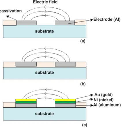
monito-ring [57]. . . 20 Figure 2.11 Simultaneous SPR and ECIS measurements setup. [58]. . . 21 Figure 2.12 Schematic of integrated sensor including the LAPS and ECIS [59]. . . 23 Figure 4.1 Basic parallel plate capacitor structure. . . 27 Figure 4.2 Sensing electrodes implemented using standard CMOS process. (a)
Topmost metal layer with removed passivation. (b) Passivated top-most metal layer. (c) Top top-most metal layer with gold deposition as a biocompatible and stable material. . . 29 Figure 4.3 CMOS-MEMS capacitive sensor with deformable and polymer-filled
Figure 4.4 Cell-electrode interface (a) T=0 , no voltage applied to the sensing electrodes,( b) T=T1 , voltage applied to the electrodes, (c) Electrode-electrolyte equivalent circuit model when there is no cells, (d) Electrode
–electrolyte model in the presence of cells. . . 32
Figure 4.5 Schematic diagram of layer-by-layer deposition of polyelectrolyte mul-tilayers [79]. . . 33
Figure 4.6 Simplified diagram of half-bridge capacitive sensor. . . 35
Figure 4.7 Simplified block diagram of a switched capacitor circuit. . . 35
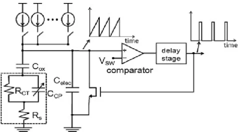
Figure 4.8 The capacitance to frequency converter : the comparator produces a digital bit stream whose frequency is inversely proportional to sensed capacitance [31]. . . 36
Figure 4.9 Capacitance to pulse-width converter for neurotransmitter dopamine detection. . . 38
Figure 4.10 Capacitance readout based on charge-sharing principle. . . 38
Figure 4.11 Charge based capacitive sensor structure. . . 39
Figure 4.12 Charge based capacitive sensor for particle detection [89]. . . 39
Figure 5.1 Illustration of CMOS capacitive sensor for Lab-on-Chip applications. 44 Figure 5.2 CBCM circuitry : (a) Basic CBCM circuit with off-chip ammeter, (b) Associated clock pulses for basic CBCM, (c)-(d) Our previously propo-sed CBCM circuitry and Σ∆modulator, (e) Input and output signals associated with Σ∆modulator. . . 45
Figure 5.3 Proposed capacitive sensing system consisting of on chip readout in-terface (interdigitated electrodes, differential core-CBCM CVC and ADC), and off-chip FPGA system (pulse generator and decoder). . . 46
Figure 5.4 Proposed fully differential CBCM architecture and input clock pulses. 47 Figure 5.5 COMSOL simulation results : (a) Capacitance variation versus dielec-tric material distance from electrodes, (b-d) : Elecdielec-trical field distribu-tion over electrodes where (b) No material is near electrodes, (c) A material exist in 1 µm proximity of electrodes, and (d) A material is attached to the electrodes. (Dimensions are mentioned in Table 5.1). 49 Figure 5.6 Σ∆ modulator (a) Ideal 1st order, (b) proposed modulator, (c) signal diagrams. . . 50
Figure 5.7 Proposed Σ∆ Modulator circuit implementation : (a) TR1, TR2 and comparator shown in Figure 5.6, (b) differential comparator implemen-tation. . . 51
100 fF and 103 fF, the output voltage is plotted for two Φ3 frequencies (4 MHz and 2 MHz). . . 51 Figure 5.9 Generated bit stream by proposed Σ∆ modulator for CS values of 101
fF, 101.01 fF and 101.02 fF. . . 52 Figure 5.10 Novel Σ∆ modulator’s main result : Decoded bit-stream generated by
Cadence simulation and imported in Matlab, CS varies between 100 fF
and 100.5 fF in 10 aF steps. This curve shows a linear relation between the decoded output bit stream and input capacitances. . . 53 Figure 5.11 Simulation results showing the effect of mismatch error on sensitivity
and dynamic range of the capacitive readout circuit. . . 54 Figure 5.12 Simulation results showing the effect of comparator non idealities on
the performance of Σ∆ modulator. . . 54 Figure 5.13 Sensitivity variation and power consumption for different values of N. 55 Figure 5.14 The maximum number of N for different integrating capacitance (Cint)
value. . . 56 Figure 5.15 Effect of N on linearity and dynamic range of the sensor, (Cint=2pF). 56 Figure 5.16 Die image and test setup : (a) Die micro photograph, (b) Capacitive
electrodes, (c) Test fixture. . . 57 Figure 5.17 Experimental set-up : FPGA platform (clock generator and decoder),
oscilloscope and Power supply, microprobe on top of the CMOS chip, and microscope. . . 57 Figure 5.18 Probe test results, output voltage variation where (a) no probe, (b)
probe is in close proximity of electrode, (c) probe is attached to the electrodes, output bitstream generated by Σ∆ modulator when : (d) no probe is on the surface, (e) probe is in close proximity of electrode, (f) probe is attached to the electrodes, (N=4). . . 59 Figure 5.19 Output voltage for different organic solutions : (a) no solution, (b)
dis-tilled water (dielectric constant : 80), (c) Acetone (dielectric constant : 20.7), (d) Methanol (dielectric constant : 33.4), (N=1). . . 60 Figure 5.20 Measured average differential output voltage changes for different
che-mical solvents : D (Dichloromethane), A (Acetone), E (Ethanol), M (Methanol), W (Water). . . 60 Figure 5.21 The average output voltage variation for different concentrations of
Figure 6.1 Illustration of recently proposed capacitive sensor for cellular analysis. (a) Cells attached on the interdigitated electrodes. (b) Simple illustra-tion of CBCM circuitry. (c) Response of the chip to adherent H1299 cells. . . 64 Figure 6.2 (a) System level block diagram of proposed cell-based capacitive
sen-sor, CSs blocks refer to interdigitated sensing electrodes, and CBCM refers to charge based capacitive measurement circuit block. (b) Circuit implementation of capacitive readout interface. . . 66 Figure 6.3 Capacitive sensor array and corresponding addressing circuit. SW switches
are controlled by 3x8 decoders and they are connecting the sensing elec-trodes to core-CBCM circuits. . . 68 Figure 6.4 (a) Simplified block diagram of calibration circuitry. (b) Latched DAC
with reset input. In each calibration clock, the output voltage is com-pared with the reference voltage, based on the difference with the refe-rence voltage, the 4-bit DACs currents charging the integrating capa-citors are adjusted. . . 69 Figure 6.5 Simulation results showing the calibration circuit performance. . . . 70 Figure 6.6 Simulation results showing the effect of number of calibration stages on
the total error in output voltage caused by mismatch between current mirror transistors in CBCM circuit . . . 70 Figure 6.7 Behavioral model algorithm developed in Matlab.Y(n) is the output
voltage, X is the constant input coming from sensing electrodes, Q(n) is the output of the quantizer for nth input sample, TQ is the sampling period, and Tf in is total sampling time. . . 72
Figure 6.8 Search for optimal parameter using behavioral model. Cint is integra-ting capacitor at CBCM output, Ain is input signal amplification factor (the gain of CBCM current mirrors), Tfin is the total sampling time that reflects the number of stored bits and Adac is the amplification factor of DAC in modulator loop. . . 74 Figure 6.9 Post layout results : FFT waveform for the DC-input modulator with
OSR=128 and sampling frequency of 1 kHz. . . 75 Figure 6.10 Post layout simulations : (a) SNDR for two inputs with DC and 0.5
Hz frequencies and for amplitudes varying between 0 to -60 dBFS. (b) SNDR measurement for input capacitance values between 1 to 10 aF. 76 Figure 6.11 Post-layout simulations : output voltage for sensing capacitance
image of interdigitated electrodes, two pairs of interdigitated electrodes are shown as E1 and E2. (c) Die microphotograph. . . 79 Figure 6.13 Measurement results showing the performance of the calibration
cir-cuit. . . 79 Figure 6.14 Sensor response to organic solvents, (a) the average response of the 64
pixel array to various chemicals including : A : Air, D : Dischlrome-thane, I : Isopropanol, M : Methanol, MD : Methanol dilution, DI : Deionized water, C : Culture media. "Sigma-delta" shows the decoded value of bit-streams coming from the output of Σ∆ modulator and "Analog" refers to the analog output voltage at integrating capacitor’s node. (b) Sensor response to the dilutions of Methanol in DI water at different working frequencies (S refers to the slope of curves). . . 81 Figure 6.15 Response of the chip to Polystyrene beads diluted in DI water, 1 k
beads/ml concentration is shown. . . 82 Figure 6.16 Response of the chip to Polystyrene beads diluted in DI water, from
10k beads/ml to 10 beads/ml dilutions are shown. . . 82 Figure 6.17 CMOS chip response to 100 k cells/ml for 12 h. . . 83 Figure 6.18 Comparison of the CMOS chip results and Alamarblue results for the
same concentration of the cells. . . 84 Figure 7.1 Simplified illustration of proposed cell-based biosensor and the
prepa-ration steps : (a) Packaging and wirebonding, (b) Layer-by-layer (LBL) coating, (c) Microwell implementation (d) Cell seeding, incubation, and monitoring. . . 89 Figure 7.2 (a) System-level block diagram of proposed cell analysis chip. (b)
Cir-cuit implementation and cell-electrode capacitance model. . . 91 Figure 7.3 (a) Schematic overview of microwell integration with CMOS chip. (b)
Placing the first PDMS layer using the flip-chip bonder, (c) PDMS layer alignment on the sensors, (d) Top glass layer placement. (e) Pressing the layers and applying epoxy to cover the wire-bonds and to attach the layers while the chip is on a hot-plate. . . 95 Figure 7.4 PEM bio-compatibility test on aluminium layers, (a) The aluminium
sheet half-covered with the PEM, (b) Fluorescence image of GFP cells cultured on the surface. (c) The cell confluency measurements for va-rious PEM coating combinations. (d) Detecting PEM formation on CMOS chip using capacitive sensor. . . 100
Figure 7.5 (a) CMOS chip results showing the response of capacitive sensors to various concentrations of H1299 cell lines, (b) Alamarblue results sho-wing the cell concentrations, (c) CMOS chip results shosho-wing the effect of Geneticin on cell growth for resistant Hek-293GFP and non-resistant H1299 cell lines, (d) Alamarblue results showing the effect of Geneticin on cell growth for resistant Hek-293GFP and non-resistant H1299 cell lines. . . 101 Figure 7.6 Optical observation of cells in (a) Standard Petri dish (before addition
of Geneticin), (b) Standard Petri dish (24 hours after addition of Ge-neticin), (c) Smart Petri dish (before addition of GeGe-neticin), (d) Smart Petri dish (24 hours after addition of Geneticin). (e) Cell counting re-sults showing the effect of antibiotic on cell number after 48 hours.
. . . 102 Figure 7.7 Cell culture monitoring using proposed 4-well microfluidic/microelectronic
platform : (a) Right after seeding the cells. (b) 4 hours after cell seeding. (c) 8 hours after cell seeding (d) Media evaporation and cell death. (e) Chip scale microscopy showing the cultured cells in the microwells. . 104
ADC Analog to Digital Converter
CBCM Charge-Based Capacitive Measurement CDC Charge to Digital Converter
CMOS Complementary Metal Oxide Semiconductor DAC Digital to Analog Converter
DC Direct Current
DMA Direct Memory Access DNA Deoxyribonucleic Acid ECG Electrocardiography
ECIS Electric Cell–Substrate Impedance Sensing EDTA Ethylenediaminetetraacetic Acid
EMEM Eagle’s Minimal Essential Medium ENOB Effective Number Of Bits
FBS Fetal Bovine Serum FET Field Effect Transistor FFT Fast Fourier Transform FIFO First In First Out
FPGA Field Programmable Gate Array IDE Interdigitated Electrode
ISFET Ion Sensitive Field Effect Transistor LAPS Light Addressable Potentiometric Sensor LoC Lab on Chip
MEA Multi Electrode Array
MEMS Micro Electro-Mechanical Systems
NMOS N Channel Metal-Oxide-Semiconductor Field Effect Transistor OSR Oversampling Ratio
PBS Phosphate-Buffered Saline PCB Printed Circuit Board PDMS Polydimethylsiloxane PEM Polyelectrolyte Multilayer
PMOS P Channel Metal-Oxide-Semiconductor Field Effect Transistor QCM Quartz Crystal Microbalance
SNDR Signal to Noise and Distortion Ratio SPR Surface Plasmon Resonance
UV Ultra-Violet
APPENDIX A BIOLOGICAL EXPERIMENTS : EQUIPMENTS AND PROTOCOLS 129 APPENDIX B CHIP PACKAGING EQUIPMENTS . . . 131
CHAPTER 1 INTRODUCTION
1.1 Motivation
Cells are fundamental unit of life and understanding the individual cell structure and behavior plays an important role in understanding more complex units such as tissues and organs. Cell culture monitoring and quantification of cellular phenotypes such as viability, growth rate, and metabolism, under controlled cell culture conditions, impact many different areas in biology and medicine. For instance, cell growth studies can be beneficial in many fields such as standardization of cell cultivation, tissue engineering, and most importantly in cancer research where the effect of certain anti-cancer drugs on the cells is of interest.
Conventionally, the cell studies and monitoring the response of populations of cells to drug candidates are performed in standard well-plates, Petri dishes, and microscopic slides. Micro-titration (MTT) analysis and fluorescence microscopy are two of the well-established methods for monitoring cellular activities and metabolism rate [1–3]. Despite the fact that these tech-niques are widely used in biological laboratories, they are time-consuming because of the required labeling, incubation, and freezing processes. In addition, they require bulky optical setups including fluorescence microscope and spectrophotometer. Moreover, some of these labeling substances are toxic and not suitable for continuous monitoring of a sample in a long period of time. To address these issues, several alternative have been proposed inclu-ding multi-electrode arrays (MEAs) [4], electric cell-substrate impedance sensing (ECIS) [5], light-addressable potentiometric sensing (LAPS) [6], and ion sensitive field effect transis-tors (ISFETs) [7]. Among them, integrated capacitance sensing technique have demonstrated interesting capability for developing miniaturized cell assays. Recent advances based on stan-dard microelectronic technologies such as CMOS process have addressed the challenge of developing high throughput, low cost, label-free, and high precision impedometric and ca-pacitive biosensors. In fact, low-cost mass production of CMOS provides the opportunity to implement scalable sensors as well as the array implementation for parallel cell detections. Despite these great advances, still the development of a large number of capacitive micro-sensors for high throughput screening is under research and cell-based biomicro-sensors still suffer from some intrinsic shortcomings. The common problems in the design and integration of cell-based biosensor are choosing the optimum dimension and topology for the sensors and the design of an efficient readout interface. The detection sensitivity of readout circuits might be limited by noise resulted from large parasitic capacitances. Furthermore, employing CMOS technology in the applications where direct contact of the sensing electrodes with the chemical
The packages should protect the device against corrosive biological solutions while it should be robust enough against several cleaning procedures and long-term cell culture experiments. Considering the tremendous future potential of lab-on-chip technologies, this thesis aims to demonstrate a new fully integrated platform that allows an efficient monitoring of cells and their physiological state in a high throughput mode while maintaining the system’s simplicity and ease of implementation. Our proposed compact, low-cost and, re-usable cell-based biosensor can be employed as a versatile tool to transit Petri dish cell-based experiments from the traditionally labor-intensive process to an automated and streamlined process which is significantly advantageous in different fields of biology and medicine.
1.2 Research hypothesis
The electrical properties of living cells and tissues have been of interest for many years. In fact all living cells, except viruses, have a similar structure including a cytoplasm surrounded by a membrane. The surface of most types of cells is negatively charged, which results in the attraction of positive ions in the growth medium to the cell surface and consequently the formation of a double layer [8]. The membrane is considered to be a highly highly non-conductive medium and its relative permittivity ranges from 2 to 10 [8]. It is reported that at low frequency fields there are two factors contributing to the dielectric properties of living cells [9].
— Reorientation of the dielectric dipoles of individual cells.
— The polarization of the surface charge accumulated on the cell membrane.
Also it has been shown that these electrical properties have a strong correlation with the morphology and health state of the cells. This means that any damage in the cell membrane can alter its dielectric properties. For this reason, the electrical properties can be used to differentiate between normal and abnormal cells and also to evaluate the cell physiological state.
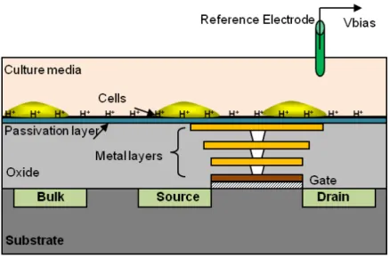
When cells are placed on an electrode, there are two phenomenas that result in a change in the sensed capacitance (Figure 1.1). The electric fields give rise to an electric dipole in the cell surface (Ccell) [10] and also a capacitive coupling happens between the electrode and the
cell’s charged membrane, which varies with the distance (Cbond). The closer the cell is to the
electrode and the stronger the cell-electrode attachment is, the value of coupling capacitance would be higher. Measuring this capacitance, can give valuable information regarding the cell-electrode interaction and the quality of cell-substrate adherence. Healthy cells have a well-formed membrane, thus sustaining a strong bond and electric dipole. However, if any
Figure 1.1: Cell-electrode capacitive model, (a) Cell suspension. (b) Adhered cells.
changes happens in the cells’ morphology and health state, for example a damage in the membrane induced by toxic agents or drugs, the electric dipole in the cell membrane will change and the bonding gets weaker.
Our assumption is that with a very high-sensitivity capacitive readout interface implemented underneath the capacitive electrodes, one can exploit the minute changes in the dielectric properties of the cells. These changes can be measured to detect the presence of the cell on the substrate and to monitor their health state. Furthermore, by continuous monitoring of capacitance changes, we can detect the presence of toxic materials and assess the effect of certain drugs on the cells.
1.3 Research objectives
The objective of this thesis is to build a fully integrated, potentially high throughput, low cost, and easily scalable tool for real-time cell analyses. We aim to build a versatile device that allows the quantitative assessment of various cell types in terms of viability and growth rate as well as their response to cytotoxic drugs. The detailed objectives are as follows.
1. To design and fabricate a cell-based capacitive biosensor array for cell viability and growth monitoring.
2. To design high performance CMOS circuits for capacitive sensor data readout and analog to digital conversion.
3. To exploit a robust packaging technique for microfluidic/microelectronic hybrid cell-based microsystem in a biocompatible process.
4. To solve the biocompatibility and non-stability issues of CMOS-based fabricated elec-trodes and to improve the bio-interface interactions at cellular level using efficient biological and chemical methods.
mated array multiplexing and readout.
6. To explore new approaches for miniaturization of microsystems by integrating micro-fluidic structures and microelectronic building blocks in a single chip.
7. To validate the proposed microsystem through measuring cell viability, proliferation rate, and response to pharmacological stimuli/drugs.
CHAPTER 2 LITERATURE REVIEW : ON-CHIP CELL MONITORING DEFINITIONS AND TECHNIQUES
2.1 Introduction
The basic in-vitro cell culture has become essential in understanding advanced cell biology and complex cellular systems such as tissues and human organs. The study of cells grown in laboratory can provide important information about cell-cell interactions, extra-cellular matrix and cell migration. In addition, these studies can be beneficial in drug toxicity scree-ning and monitoring cellular responses to a variety of different stimuli and drugs. In this chapter we introduce the essential parameters to be measured in cell culture samples and conventional methods for acquiring them along with their limitations and shortcomings. In addition, we will review the recent advances in electrochemical and non-electrochemical bio-sensing technologies that can be integrated with a standard cell culture environment. The advantages and limitations of these methods will be discussed as well.
2.2 Key parameters in cell culture monitoring
Based on the nature of biological or medical applications, there are several parameters in a cell culture sample that are important to study. They can be classified as follows.
— Metabolic activity
Living organisms require chemical energy to perform their daily activities and to maintain their viability and growing. In living cells, this chemical energy is derived from a molecule called Adenosine Triphosphate (ATP). Measuring the ATP levels in cells can give critical information about their health state. In addition, to find out more about the quality of cell metabolism and its health condition, the following parameters are of interest [11].
— Extracellular oxygen (O2) : indicates the cell respiration.
— Extracellular carbon dioxide (CO2) : reflects the cell overall viability.
— Extracellular glucose : shows the cell’s capacity to produce fuel. — Intracellular ATP : indicates how much fuel is available to the cell. — Extracellular pH : indicates cellular respiration and acidification rate. — Electro-physiological parameters
In electrophysiology, the study of ion channels has a great importance. Ion channels are transmembrane proteins that allow passage of ions through pores across a
non-great importance in cell physiology. Defective ion channels are responsible for various health problems such as cardiac or neuronal diseases [12].
— Cell signaling
Communication and signaling between cells are crucial in understanding the cells and organs functions. Several types of cell signaling exist such as neurotransmitters, antigens triggering/ antibody responses, and cell response to specific hormones [13]. These parameters in cell signaling studies can be investigated using cell-based assays. — Cell adhesion
Cell adhesion is the ability of a single cell to stick to another cells, substrates or ex-tracellular matrix (ECM). Adhesion of cells is essential in inter-cellular communication and also in the development of tissues and body organs. Any changes in the quality of cell adhesion can be a sign of wide range of diseases such as arthritis, cancer, and osteoporosis. Since most mammalian cells are anchorage-dependent and stick firmly to suitable substrates, it is important to study the quality of this attachment in various fields of bio-material studies, implantable devices, tissue-on-a-chip, and organ-on-a-chip, cancer metastasis, and drug treatments [14–16].
— Cell viability, proliferation, and cytotoxicity monitoring
The viability levels and growth rate of cells in a sample are a good indicator of their health state. The proliferation and viability assessment is usually coupled with meta-bolism analyses which is essential in cell growth measurements. On the other hand, in pharmacological profiling of drugs, it is important to investigate the interactions between the cells and drugs quantitatively. Moreover, in cancer research, the study of chemical compounds that inhibit or promote the viability of cells and their pro-liferation has a great importance [17]. In order to perform drug screening test, it is important to have a high throughout platform in order to reduce the sample consump-tion and to improve the resoluconsump-tion and sensitivity.
Due to the importance of understanding cell-surface interactions and cell growth cha-racteristics, our main focus in this thesis is measuring the cell adhesion, proliferation, and response to toxic drugs.
2.3 Conventional techniques for cell viability and growth monitoring
Among various techniques that exist for acquiring cell culture parameters, optical techniques and particularly fluorescence imaging has proven to be an inevitable tool for monitoring living cell samples. In optical assays, the cells are tagged with fluorescence dyes (fluorophores) and
based on the metabolic activity of cells, different colorimetric properties are observed [18]. This method requires special handling and treatment of cell cultures with fluorescent labels as well as the use of off-chip optics such as fluorescence microscopy and spectrophotometer. Another convenient technique is microculture tetrazolium (MTT) assay which provides a good estimation of cell viability in a sample based on colorimetric principle. MTT is a yellow water-soluble tetrazolium dye that is reduced by live cells to produce a purple formazan pro-duct that is insoluble in aqueous solutions [19]. The use of this assay requires the cultivation of cells into multiwell plates and the addition of a drug or toxin at certain concentrations for a specified amount of time. This assay is an example of a lengthy procedure that employs conventional cell culturing techniques for cell studies.
As was mentioned earlier, the cells require ATP to maintain their viability and health. During the cell death, the ATP levels falls to the points where cells can no longer maintain their metabolic activity. Therefore, a low ATP level is used as an important indicator of cell death. In contrast, any increase in the ATP levels is a direct indicator of cell proliferation and growing. In ATP assays, the bioluminescent detection of the ATP is performed for viability monitoring [20]. In this technique, a reagent called Luciferase is used to catalyze the formation of light from ATP and Luciferin that generates photons. Studies show that ATP assays have a better sensitivity, particularly for viability measurement of very low cell numbers compared to MTT assay [21].
Another technique to measure cell viability and proliferation is the use of Alamarblue reagent. The active ingredients in Alamarblue is Resazurin which is a cell-permeable blue component that is naturally non-fluorescent. Upon entering the cell membrane, it is converted to Re-sorufin, which is a bright red fluorescent compound. To perform viability tests, a certain concentration of Alamarblue is added to the cell culture wells and at certain time intervals, the reduction of Alamarblue is measured by fluorescence readings [22].
The reported assays are widely used in biological laboratories and have been very successful in cell culture monitoring. However, they all require external optical setups. Moreover, most of these methods do not provide a continuous monitoring and the measurement needs to be taken at certain time intervals after following several preparation steps. On the contrary, cell-based microsystems can provide efficient solutions to these problems by integrating and automating the sensing, readout and analyses processes in one single device. These features result in a noticeable reduction in infrastructure requirements, and measurement complexity.
nitoring
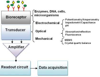
In last recent years, biosensors have rapidly expanded and evolved in many fields of biology, medicine, environmental monitoring, and nanotechnologies. These devices, by utilizing biolo-gically driven sensing elements, detect the presence of specific target analytes such as DNA, proteins, hormones, bacterias or living cells. The interaction of these analytes with the sensor interface brings about some physiochemical changes. These changes that correlate with the presence of a target analyte, can be further detected and measured by a transducer for which a transduction scheme is normally chosen based on the type of parameters to be measured such as electrochemical, mass, optical, pH, etc (Figure 2.1).
Among various types of biosensors, cell-based biosensors that measure electrochemical signals such as voltage, current or impedance, resulting from cell activity and metabolism, have become a focus of research in recent years. The living cells can be seen as an electrochemical dynamic system in which several reduction-oxidation (redox) reactions and changes of ionic composition and concentration happen. These changes which are direct indicator of cell growth and development, result in the electron generation and charge transfer which can be detected using electrochemical methods. In this regard, several biochemical parameters such as ion concentrations (H+, K+, N a+, Ca+, Cl−, etc.), membrane potential, adhesion, and morphology can be detected by electrochemical biosensors.
In the remaining of this chapter we will briefly introduce various types of integrated cell-based biosensors aimed for cell adhesion, proliferation, and drug cytotoxicity monitoring.
2.4.1 Electric cell-substrate impedance sensing (ECIS)
ECIS is one the most efficient techniques for monitoring cell adhesion, spreading, and mor-phology in real-time. The measurement principle is based on the fact that as mammalian cells attach and spread on the surface of a gold electrode, they hinder the current flow and charge transfer between the electrodes which results in an increase in the overall electrode output impedance [23]. Impedometric biosensors are divided into two categories of farai-dic and non-faraifarai-dic sensors. Faraifarai-dic detection involves the charge transfer detection in the electrode-cell interface. On the contrary, in non-faraidic schemes there is no charge transfer between the electrode and test samples and instead the transient current that is charging the capacitive electrodes is measured. Thus non-faraidic impedometric sensors are usually referred as capacitive sensors [24] which will be discussed later in details in chapter 3. Figure 2.2 shows a schematic overview of the impedance measurement setup pioneered by
Figure 2.1: Simplified block diagram of a biosensor and its conversion schemes.
Figure 2.2: Schematic overview of ECIS technique for cell adhesion detection.
Giaever and Keese [25]. In this sensing scheme, an alternating current is applied to the electrodes and the voltage is recorded using a lock-in amplifier. When there is no cell, the current flows freely on the electrodes, however as the cell, which are insulator in nature, attach
Conventionally, two electrode structures are used to realize impedometric systems, planar (monoploar electrodes) or interdigitated electrodes (IDEs). In planar architecture, usually a large counter electrode should be used for precise impedance measurements resulting in a large sensing area and a reduced sensitivity. In addition, the use of large counter electrodes makes the integration and array implementation of the ECIS difficult ; thus it is not suitable for high throughput cell-based measurements. On the contrary, in interdigitated electrodes, current flows in close proximity of the electrode surface, resulting in a higher sensing sensitivity and improved performance.
The fabrication process of ECIS consists of a metallic layer deposition on the substrate, followed by lithography and etching process. Despite the great advantage of this technique in comparison with optical techniques, it requires off-chip readout system that limits the number of input channels and consequently the number of sensing sites. Consequently, ECIS is not the best solution for high throughput applications that require a large number of multiplexed sensors. To overcome this problem, recent advances in standard microelectronic technologies such as CMOS have addressed the challenge by developing high throughput low cost label-free and high precision impedometric and capacitive biosensors [26], [27].
2.4.2 Capacitive sensing
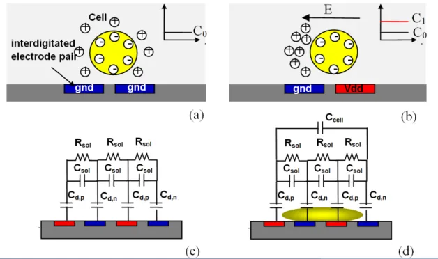
Capacitive sensors operation principle is based on the modulation of capacitance value by physical or chemical parameters’ variation. Due to their high resolution, reliability, and low temperature dependence, these types of sensors are widely used in various applications such as pressure sensing [28], accelerometers [29], humidity measurements [30], and molecular/cellular biology [31]. Since capacitive sensors have no static power consumption, they are suitable for use in energy-constrained applications, such as low-power battery-operated systems, point of care devices, and wireless sensor networks. Among different implementation of capacitive sen-sors, the development of miniaturized integrated capacitive arrays has a crucial importance for the successful employment of these microsystems in practical chemical and biological applications such as DNA hybridization detection [31], cellular studies [32], and protein in-teractions quantification [33]. There are two technical advantages in using fully integrated capacitive sensors ; the use of fully electronic circuitries allows the signal processing in close proximity of the sensors which results in a very high sensitivity and noise immunity. Mo-reover, using CMOS technology allows the integration of large number of electrodes on a single die which allows high throughput mode measurements. In addition, by using digital addressing and multiplexing techniques, integrated arrays of capacitive sensors require only
Figure 2.3: Schematic overview of capacitive technique for cell adhesion and growth monito-ring.
a few electrical wirings to off-chip interfaces that can notably reduce the number of pins and packaging costs as well.
In cell monitoring, when cells are placed above the capacitive electrodes, they start attaching and spreading over the electrodes and increasing the total capacitance (Figure 2.3). As they start spreading and growing above the electrodes, the value of sensed capacitance increases. Any changes in the cells health state induced by addition of certain drugs or chemicals that lead to detachment of the cells, results in a decrease in the capacitance value.
2.4.3 Light-addressable potentiometric sensor (LAPS)
LAPS is a newly developed semiconductor device which was first proposed by Hafeman et al. in 1988 [34]. The device is used to monitor extracellular potentials in electrogenic cells and cell metabolism rate. The simplified overview of a typical LAPS device is shown in Fi-gure 2.4. Based on electrolyte- insulator-semiconductor (EIS) or electrolyte-metal-insulator-semiconductor (EMIS) structure, a modulated external light source can be used to generate a photocurrent corresponding to the potential on Si3N4 surface. An external DC bias voltage
is applied to form a depletion layer at the interface of insulator (SiO2) and semiconductor.
Upon a change in the chemical or biological properties of electrolyte, the surface potential that reflects electrical charge at the electrolyte-solid interface is altered.When a light source is applied to the substrate, the light induced charge carriers contribute to the generation of a photocurrent. The current amplitude depends on the surface potential and can be detected by an external readout circuitry.
semicon-Figure 2.4: Schematic diagram of a LAPS measurement setup.
ductor surface, the extracellular potentials of electrogenic cells coupled to the LAPS can be monitored by surface potential alteration, which allows measuring the extracellular poten-tials at different positions on the sensor’s surface. Based on this theory, various LAPS devices have been constructed for different cell-based applications including cellular metabolism de-tection, cytotoxicity evaluation, and detection of various electrogenic cells such as cardiac, neural, and olfactory cells [35–37].
For its simple structure, the fabrication and encapsulation of LAPS is easier than other electrochemical biosensors, especially for extracellular measurements. Moreover due to the extremely flat surface, the integration of microfluidic channels with the electrode is less critical [38]. Despite the excellent integration properties of LAPS, the signal-to-noise ratio of the measured signals is low and the range of baseline drift is wide, especially in the detection of signals fired by neurons. These factors limit the application of LAPS in neural studies. To improve the performance, certain signal processing techniques such as wavelet transform denoising are proposed. They can partially cancel out the background noise [39].
2.4.4 Ion-sensitive field effect transistor (ISFET)
The ISFET invented by Bergveld in 1970 [40], is a chemically sensitive field effect transistor. As shown in Figure 2.5 it can be described as a MOSFET with the gate connection separated from the chip and inserted in an aqueous solution referred as reference electrode. Due to its small size, rapid pH response, repeatability, low process variation, and low cost construction,
Figure 2.5: Schematic diagram of ISFET pH-sensor, the gate is connected to the pH-sensitive membrane by stacking metal layers.
the ISFET is widely used for electrochemical detections.
The standard ISFET structure has an insulating membrane which is sensitive to hydrogen ions in the test solution. As a result, any charge build-up on the membrane, which varies with pH solution, causes a modulation of the ISFETs threshold voltage.
ISFETs can be fabricated in standard CMOS process following the exact steps for MOSFET fabrication, which is referred as ISFETs in unmodified CMOS process [41]. This process em-ploys a floating-electrode design. All the metal layers in the process are connected together with vias, allowing the silicon nitride passivation layer to act as the pH-sensitive membrane. Silicon nitride is well known for ISFET fabrication and gives a linear response, with sen-sitivity in the range of 45-56 mV/pH [42]. If ISFET is used as a pH sensor only, no extra processing step for membrane modification is required. However making the ISFET sensitive and selective to other ions such as N a+, K+ and Ca+, requires extra steps for the deposition
of membranes [43, 44].
The fabrication of floating gate ISFETs in standard CMOS process leads to some non-idealities including the accumulation of trapped charge on the gate and passivation layer during the fabrication process. The presence of trapped charge can result in a large and un-predictable variation in ISFET threshold voltage. However the excess charges can be removed by UV radiation and hot electron injection techniques [45, 46].
Figure 2.6: Schematic diagram showing the mechanism of cell-based assays employing QCM devices [47].
2.4.5 Quartz crystal microbalance (QCM)
QCM is a type of label-free acoustic sensor that is used in various physical, chemical and biological applications. By measuring the mass and energy dissipation of the materials on the sensor surface, it has been applied in various cell-based assays for studying the cell-cell and cell-surface interactions [48, 49]. The simplified schematic of a QCM sensor is shown in Figure 2.6. The main component of the device is a quartz crystal which is placed between two metal electrodes. The signal transduction mechanism of the QCM devices is based on converse piezoelectric principle in which electrical charges are generated on opposite sides of a crystalline substance upon its mechanical deformation [49]. By applying an alternating current (AC) to the pair of metal electrodes which are sandwiching the crystal, an oscilla-tion in the quartz crystal happens which its frequency is linearly proporoscilla-tional to the mass above the electrodes [50]. By employing QCMs and measuring the changes in the oscillation frequency, the attachment and spreading of the cells above the gold electrodes can be moni-tored. In addition, this type of biosensor can be potentially useful in identifying active drug compounds that affect cell attachment and proliferation specially in cancer cell studies when the sensitivity of the cells to anticancer drugs is of interest [51].
2.4.6 Surface plasmon resonance (SPR)
Surface plasmon resonance (SPR) is an optical biosensor that is used to detect the changes in physio-chemical properties of the solution-sensor interface. By using the refractive index of the analyte on the sensor’s surface, this method allows the quantification of several bio-moelcular and cellular interactions. Although it is mostly used for molecular research and analysis of the bio-molecules, it can be employed to study the interactions between the living
Figure 2.7: Schematic overview of Surface plasmon resonance (SPR) sensors which detect a refractive index change within a detection area (<500 nm) as a change of resonance angle caused by the cell attachment.
cells and to analyze the molecules that induce any reactions from cells [52].
The principle of operation is based on the fact that when a light beam hits an interface of two transparent medias (e.g. a glass prism and a solution), the light is partly reflected from the media with the highest refractive index (glass prism) [53]. In SPR devices one side of the glass prism is coated with thin Au layer (Figure 2.7). The light excites the free electrons at the metal surface (known as surface plasmons) and makes them oscillate. Some of these plasmon particles are confined on the metal surface, creating an electric field that extends a few tenth of nanometer into the buffer, Au film, and the prism and is called evanescent wave. If any changes happens in the metal surface property, such as interaction of target and probe molecule, the momentum of the plasmons and their evanescent fields will alter and a shift in the incidence light reflection angle will happen. The shift in the resonance angle is directly proportional to the density of biological molecules in the evanescent field thus it can detect the association and dissociation of biological molecules on a gold surface with no labelling process needed.
Despite the other types of biosensors, SPR can also reveal valuable information about sub-cellular structures with high temporal and spatial resolutions and can be used as a powerful tool for intracellular studies [54].
In previous section we briefly reviewed some of the most widely used techniques in cell studies. It is worth mentioning that great progress in biology and medicine relies on convenient and traditional techniques such as MTT analysis, viability reagents (such as Alamarblue or Trypan blue) and fluorescence microscopy. These techniques are employed as the most standard assays for monitoring cellular activities and metabolism rate. Despite their great performance, they have some drawbacks such as processing time, bulky instrumentation, and discontinuous measurements.
As an alternative to traditional methods several techniques have been proposed including ECIS, capacitive, ISFETs, LAPS, QCM, and SPR sensors which were briefly reported above. The advantage of standard microelectronic technologies, particularly CMOS, is the fact that they allow a monolithic integration of large numbers of micro-sensors along with their asso-ciated electronic circuitry for creating a single device capable of performing several cell-based experiments. The comparison between these methods is summarized in Table. 2.1. It is worth mentioning that each of these techniques has its own advantages in specific cell-based appli-cation and selecting among them strongly depends on the type of parameters to be measured. For example, for extracellular pH and cell metabolism monitoring ISFETs and LAPS are the best candidates, although they might require external reference electrodes for the former and external light sources for the latter. For the applications that rely on the quality of cell-substrate adhesion, ECIS and capacitive measurements are suitable alternatives while these two techniques cannot be used for non-adherent cells measurements. Since most mammalian cells are anchorage dependent which means that they need to attach to the substrate in order to growth and maintain their life cycle. Understanding cell-substrate interaction has a great importance in medical and bioengineering applications. In this regard, capacitive and impedometric cell culture platforms are capable of analyzing several cell events including cell adherence, spreading, proliferation, and death quantitatively.
2.5 Integrated biosensors for cell viability, growth, and cytotoxicity monitoring : A review.
In previous section we introduced the most well-known electrochemical, optical, and mecha-nical techniques for cell analyses. We finish this chapter by reviewing the state of the art of these technologies with the focus on cell viability, growth, and cytotoxicity monitoring. Various advanced technologies and techniques including microelectronic, microfluidic, surface functionalization, and packaging are required to realize an efficient cell-based microsystem.
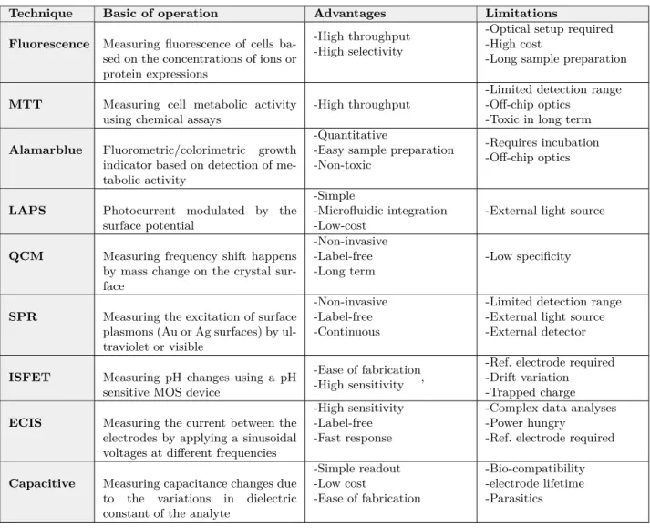
Table 2.1: Comparison of electrochemical and non-electrochemical cell analyses techniques
Technique Basic of operation Advantages Limitations
Fluorescence Measuring fluorescence of cells
ba-sed on the concentrations of ions or protein expressions
-High throughput -High selectivity
-Optical setup required -High cost
-Long sample preparation
MTT Measuring cell metabolic activity using chemical assays
-High throughput
-Limited detection range -Off-chip optics
-Toxic in long term
Alamarblue Fluorometric/colorimetric growth
indicator based on detection of me-tabolic activity
-Quantitative
-Easy sample preparation -Non-toxic
-Requires incubation -Off-chip optics
LAPS Photocurrent modulated by the surface potential
-Simple
-Microfluidic integration -Low-cost
-External light source
QCM Measuring frequency shift happens by mass change on the crystal sur-face
-Non-invasive -Label-free -Long term
-Low specificity
SPR Measuring the excitation of surface plasmons (Au or Ag surfaces) by ul-traviolet or visible
-Non-invasive -Label-free -Continuous
-Limited detection range -External light source -External detector
ISFET Measuring pH changes using a pH
sensitive MOS device
-Ease of fabrication -High sensitivity ,
-Ref. electrode required -Drift variation -Trapped charge
ECIS Measuring the current between the electrodes by applying a sinusoidal voltages at different frequencies
-High sensitivity -Label-free -Fast response
-Complex data analyses -Power hungry
-Ref. electrode required
Capacitive Measuring capacitance changes due
to the variations in dielectric constant of the analyte
-Simple readout -Low cost -Ease of fabrication -Bio-compatibility -electrode lifetime -Parasitics
We will also review the pros and cons of these platforms in terms of CMOS integration capability, ease of implementation, and accuracy.
2.5.1 Case study 1 : Multichannel lens-free CMOS sensors for real-time moni-toring of cell growth
In [55] a platform for real-time monitoring of cells is proposed that is realized by integration of a three-layer poly-methyl methacrylate (PMMA) cell culture microchip and a multichannel lens-free CMOS/ Light-emitting diode (LED) imaging system.
Figure 2.8 shows the schematic illustration of this platform for real-time cell growth imaging. The PMMA microchip consists of three layers in which the top layer contains a circular hole for the installation of the cell culture medium tube and the two other layers are used to
ba-(a) (b)
Figure 2.8: (a) Schematic illustration of lens free CMOS-based imaging system. (b) Compa-rison of images acquired by CMOS-based imaging system (top) and traditional microscope with 40x magnification (bottom) [55].
lance the air pressure. The monitoring system consists of four CMOS image sensors arranged in a rectangular array on a lower PMMA substrate and four LED white light sources placed on the upper PMMA substrate above the corresponding CMOS image sensors. The LED light sources and CMOS sensors are controlled using a program in LabVIEW. Using a custom-designed interface, the light sources and sensors are turned on at predetermined 30 min intervals and at the end of image acquisition they are tuned off. For imaging, commercially-available CMOS image sensors are used. The feasibility of the imaging system is investigated by using various concentrations of HepG2 cell lines. For each samples, the cells are cultivated for a period of 48 h and a series of images is acquired at 8 h intervals. Cytotoxicity tests were also performed in which the HepG2 samples were seeded in the microfluidic cell culture chip for 24 h and were treated with cyclophosphamide and then monitored for a further 24 h. The results show that while the untreated cells grow steadily over time, the treated cells exhibit a decreased growth rate as a result of cytotoxic drug.
This work shows a good example of real-time cell growth monitoring using CMOS-based optical techniques. The results obtained from the lens-less CMOS imaging system are in good agreement with a conventional microscope under 40x magnification. Despite the good performance of the system as a low throughput array, because of the passive substrate used for integration, the device is not applicable in high throughput applications where a higher number of sensors is required. The alignment of LEDs on the top PMMA layer with the image sensors on the bottom plate can be difficult especially when integrating a large number of
sensors on a limited substrate space.
2.5.2 Case study 2 : High density CMOS electrode array for high throughput and automated cell counting
In another effort in [56], a high-density biosensor array based on electrical-impedance spec-troscopy (EIS) is developed for real-time cell counting. This biosensor, aimed to detect breast tumor MCF-7 cells, consists of an array of 96 x 96 densely placed electrodes fabricated in 0.18 µm CMOS technology. Each single electrode is addressable by using an underneath multiplexing circuitry. The exposed Al electrodes (22 µm x 22 µm) are post processed and 100 nm of titanium (Ti) and 1 µm of gold (Au) are deposited on the electrodes by standard photolitography process. The addressing and impedance readout circuitry are used off-chip (Figure 2.9) and are controlled by LabVIEW. To encapsulate the chip and to provide a cham-ber for containing the solution, a glop top bio-compatible silicone encapsulants is used. To realize the counter electrode for impedance measurement, an indium-tin-oxide (ITO) coated glass is positioned on top of the chamber to act as a counter electrode. In the proposed chip, the impedance readings are based on the binary “on” and “off” response and the presence/ absence of the cells is detected by the recorded impedance value.
Although this platform has the advantage of high-density electrodes, it suffers from a couple of limitations ; first, due to the use of off-chip LCR meter, the sensitivity and resolution of the impedance readings is low, thus only a binary signal showing the presence or absence of the cells is obtained. Second, the need for ITO glass electrode, makes the integration of the proposed platform difficult and its not very suitable for portable and point of care diagnostics. However, due to the simplicity in the design and high-density of electrodes, the device is a suitable candidate for short term cell counting applications where only the number of cells in a sample is of interest.
2.5.3 Case study 3 : CMOS capacitive sensor for viability and proliferation monitoring
As was discussed earlier, label-free capacitive sensors are one of the most efficient alterna-tives for cell viability monitoring. In this regards Prakash et al. developed a CMOS capacitive sensor for cell viability and proliferation monitoring [32, 57]. In this platform, the working principle is based on measuring the changes in capacitive coupling between the sensing elec-trodes and cultured cells resulted from the adhesion of cells. As mentioned in this paper, when cells are placed in low frequency electric fields, the ionic cloud surrounding the cells membrane is polarized giving rise to electric dipoles. For healthier cells, the value of this
Figure 2.9: Electrical-impedance spectroscopy (EIS) platform for tumor cell counting. (a) micro-photograph of the fabricated chip.(b) Image of post-processed micro-electrode. (c) SEM micrograph of microelectrode with 6 stacks of metal layers. (d) CMOS chip in a PGA carrier mounted on the PCB [56].
Figure 2.10: CMOS cell-based biosensor for cell viability and proliferation monitoring [57].
capacitance is higher [10]. The capacitance measurement is based on the charge sharing principle. The sensor chip is mounted on a DIP40 ceramic package and encapsulated using biocompatible polymer. A typical well (diameter = 1.5 cm, height = 0.5 cm) is attached on top of the packaged chip for containing the cell culture medium. The platform is used for on-line tracking of human MDA-MB-231 breast cancer cell proliferation, with a sensor chip
that is fabricated in a 0.5 µm CMOS technology. During the cell adhesion and forthcoming proliferation the sensor recorded capacitance variations in a range of a few fF.
Despite the other presented LoC devices, this platform is fully integrated employing CMOS technology and thanks to its high sensitivity, it is a good example of a continuous measure-ment setup for cell proliferation monitoring. The work can be further optimized by increasing the array size and adding microfluidics for high throughput measurements.
2.5.4 Case study 4 : Label-free monitoring of cell-based assays : Combining impedance analysis with SPR for multiparametric cell profiling
In another effort in [58], a two-parameter cell-based sensor is developed monitoring the elec-trical and optical changes in cell sample, simultaneously. The dual sensor platform is imple-mented by integrating both techniques, ECIS and SPR, on a single sensor chip. The proposed system is based on the commercially available SPR substrate with high refractive index glass slides that is covered with a gold layer on top. The gold layer is structured by standard photolithography and wet etching (Figure 2.11). After realizing electrodes on the SPR chip, a biocompatible flow chamber is glued on the top which is made of PDMS with the fluid volume of approximately 500 µm. The sensor surface features two addressable circular wor-king electrodes and one shared large counter electrodes which used for SPR measurement as well. The SPR measurements are performed with an off-chip device and the impedance measurements are conducted via a commercially available impedance analyzer. In described work, the proof of concept experiments are mostly focused on MDCK II (Madin-Darby ca-nine kidney, strain II) cell attachment and spreading as well as cytotoxicity monitoring of actin cytoskeleton disrupting drug [58].
The combination of SPR with ECIS technique is a powerful tool to obtain complementary parameters from a cell sample while requiring no reagent preparation and labelling process.
![Figure 2.10: CMOS cell-based biosensor for cell viability and proliferation monitoring [57].](https://thumb-eu.123doks.com/thumbv2/123doknet/2341339.33916/41.918.296.613.526.870/figure-cmos-cell-based-biosensor-viability-proliferation-monitoring.webp)
![Figure 2.12: Schematic of integrated sensor including the LAPS and ECIS [59].](https://thumb-eu.123doks.com/thumbv2/123doknet/2341339.33916/44.918.137.784.105.317/figure-schematic-integrated-sensor-including-laps-ecis.webp)
![Figure 4.8: The capacitance to frequency converter : the comparator produces a digital bit stream whose frequency is inversely proportional to sensed capacitance [31].](https://thumb-eu.123doks.com/thumbv2/123doknet/2341339.33916/57.918.211.702.101.469/capacitance-frequency-converter-comparator-frequency-inversely-proportional-capacitance.webp)