HAL Id: hal-02281097
https://hal.archives-ouvertes.fr/hal-02281097
Submitted on 7 Sep 2019
HAL is a multi-disciplinary open access archive for the deposit and dissemination of sci-entific research documents, whether they are pub-lished or not. The documents may come from teaching and research institutions in France or abroad, or from public or private research centers.
L’archive ouverte pluridisciplinaire HAL, est destinée au dépôt et à la diffusion de documents scientifiques de niveau recherche, publiés ou non, émanant des établissements d’enseignement et de recherche français ou étrangers, des laboratoires publics ou privés.
Building a near-field scanning millimeter-wave
microscope integrated in a scanning electron microscope
Petr Polovodov, Olaf Haenssler, Didier Theron, Christophe Boyaval, Sophie
Eliet, Gilles Dambrine, Kamel Haddadi
To cite this version:
Petr Polovodov, Olaf Haenssler, Didier Theron, Christophe Boyaval, Sophie Eliet, et al.. Building a near-field scanning millimeter-wave microscope integrated in a scanning electron microscope. Inter-national Conference on Manipulation, Automation, and Robotics at Small Scales, MARSS 2019, Jul 2019, Helsinki, Finland. 3 p. �hal-02281097�
Building a near-field scanning millimeter-wave microscope
integrated in a scanning electron microscope
1Petr Polovodov, 2Olaf Haenssler, 1Didier Théron, 1Christophe Boyaval, 1Sophie Eliet, 1Gilles Dambrine and 1Kamel Haddadi
1University Lille, CNRS, UMR 8520 - IEMN, F-59000 Lille, France 2University of Oldenburg, Oldenburg, Germany
Abstract — A near-field scanning millimeter-wave frequency
microscope built inside a scanning electron microscope is described. The proposed instrumentation can provide simultaneous atomic force and millimeter-wave images together with the scanning electron microscopy image of the probe / sample interaction. In contrast with conventional scanning microwave microscopy tools, the instrumentation proposed opens the way to achieve traceable measurements by tackling issues encountered in traditional near-field scanning microwave microscopy tools. First, water meniscus in the vicinity of the probe tip is eliminated to reduce parasitic capacitance. Secondly, targeted frequency up to 110 GHz results in confined electric fields in the vicinity of the probe tip to enhance the lateral resolution. Finally, visualization of the tip / sample interaction offers unique possibility to support the measured millimeter-wave signals by fine FEM modeling.
Keywords — Near-field scanning microwave microscopy (NSMM), scanning electron microscope (SEM), evanescent waves, millimeter-wave.
I. INTRODUCTION
The introduction of near-field scanning microwave microscopy (NSMM) tools have pioneered many applications, notably including mapping and quantitative measurement of the electrical properties of materials and devices at micro and nano scale [1]-[7]. Basically, the scanning microwave microscope (SMM) consists of an atomic or scanning tunneling microscope combined with a vector network analyzer (VNA) [8]-[9]. The tip scans across the sample, emitting a microwave signal scattered by the material, altering its amplitude or/and phase properties.
Most of the reported NSMM tools operate in the microwave frequency range, i.e. 300MHz-30GHz. Consequently, there is a natural mismatch between the probe tip size (tens of nm) compared to the wavelength of operation in the order of the cm. When the tip of the probe is held close to the surface of a sample, at a distance separation much smaller than the wavelength of operation, the evanescent electric fields are highly confined in space. In contrast with traditional methods based on propagating waves, microscopy techniques result in high lateral and depth resolutions governed by the tip size [10]-[13]
There is an urgent need to extend the frequency capabilities of microwave microscopy tools to achieve sub-50nm spatial resolution combined with sub-aF electrical resolution. In this effort, a new NSMM is developed with broadband
capabilities up to 110 GHz. Consequently, the new instrumentation offers the possibilities to adapt the lateral and depth resolutions by proper choice of the frequency of interest in the range 1-110 GHz. In addition, the instrumentation has been designed to operate inside a scanning electron microscope for environment control and water meniscus elimination [14]-[15]. Finally, SEM image of the tip / sample interaction offers the opportunity to achieve fine FEM modeling [16]-[17]. In Section II, the design, fabrication and validation of the probing structure is presented with a preliminary targeted frequency of 40 GHz. In Section III, the system integration that requires specific design considerations is discussed.
II. MICROSTRIP PROBING STRUCTURE
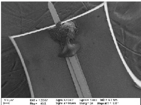
The NSMM-cantilever consists of a modified 12Pt400B microwave probe from Rocky Mountain Nanotechnology® (RMN) to achieve 40 GHz frequency operation. This probe consists initially in an ultra-sharp solid platinum probe tapered down to 50 nm and attached to a ceramic substrate. The probe is modified to support a TEM propagation mode through a microstrip structure. To that end, a conductive gold line of 200 µm is placed under the platinum, and continues to the back of the chip as the transmission line (Fig. 1). The back side is then completely covered with gold over an adhesive layer. This NSMM-Cantilever is embedded into a waveguide structure (both coplanar and microstrip structures have been realized for further comparisons) which can be exchanged in case of destroyed tips by using a solder-less PCB mount connector of Rosenberger Corp. with a clamping and screwing mechanism (Fig. 2).
Fig. 1. Scanning electron image of the NSMM-cantilever manufactured by RMN®.
Fig. 2. NSMM-cantilever integration in a dedicated PCB board.
The NSMM-probe has been assembled and millimeter-wave characterization has been performed using a vector network analyzer to measure the return loss (Fig. 3).
Fig. 3. Return loss mag(S11) of the modified NSMM-probe.
From the experimental results, Fig.3 shows magnitude of the reflection coefficient better than -10 dB up to 40 GHz in accordance with simulated data (not shown here). It has to be noticed that that three resonances occur in the measured response. A time-domain analysis has been used to identify the origins of the resonances at 7.7GHz: transition connector-substrate, 23.1 GHz: Cantilever beam and 37.8 GHz: transition substrate-cantilever. Although the impact of the resonances is minor, optimization of the transitions is under investigation to limit resonance effects.
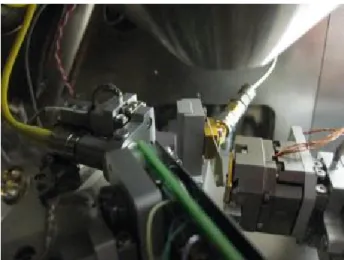
III. SYSTEM INTEGRATION
The block diagram of the system is described in Figure 4. The hemisphere above the sample is mainly occupied by the electron column and leaves only a very small gap accessible
for the SMM to achieve a working distance of 20 mm. The system presented here has been designed to be as compact as possible. The SMM stage is mounted on the chamber vertically to the electron beam of the SEM. The SMM consists of two main components, a sample scanning stage and a probing unit (Fig. 4). The sample scanning stage is composed of an AFM scanner positioned onto a coarse positioning stage. The positioning stage consists of three piezo driven linear actuators manufactured by Smaract GmbH with scanning ranges of 26 mm in X and Y directions and 11 mm in Z direction. The actuators enable closed-loop operation with less than 10 nm resolution and 25 nm repeatability in any direction. The AFM scanner ANSxyz100/Std from AttocubeTM operates in open-loop on scanning ranges of 505024 µm3 with sub-nm positioning resolution and 0.1% scan repeatability (Fig. 5).
Fig. 4. Sketch of the proposed millimeter-wave NSMM.
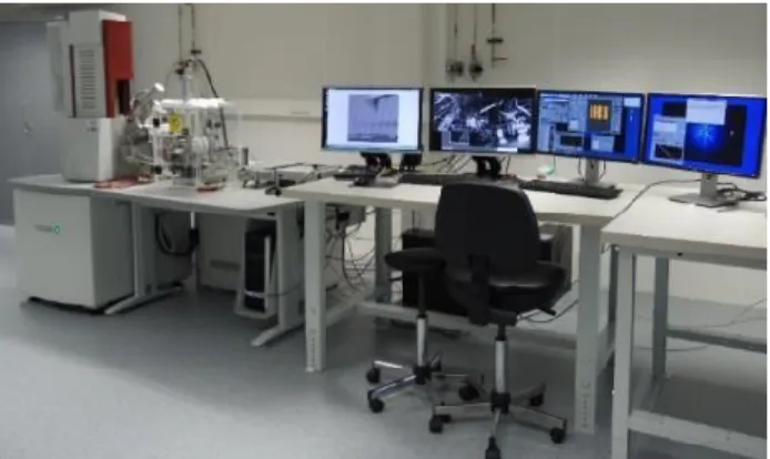
Fig. 5. Photography of the millimeter-wave NSMM integrated inside a Tescan Mira XMU SEM.
The measuring equipment, i.e. SMM integrated into SEM, has been developed and is operational. Fig. 6 gives a picture of the equipment.
Fig. 6. Millimeter-wave NSMM integrated into a SEM.
The preliminary experimental demonstration considers the capacitance reference kit developed my MC2 Technologies® and uses a modified probe from Rocky Mountain Nanotechnologies® [Fig7(a)]. The topography, amplitude and phase images are simultaneously scanned over 30 x 30 µm2 at the scan rate of 5.8 µm/s (0.19 line/s in a single direction) with 512 x 512 pixels resolution. Fig. 7(b) demonstrates 2D AFM image of the reference kit of the device under test.
(a) (b)
Fig. 7. (a) 25Pt300D modified Rocky Mountain Nanotechnologies® [spring constant = 18 N/m (± 40%)]. (b) 2D 30×30 µm2 image on reference sample (Capacitance reference kit
from MC2 Technologies®).
IV. CONCLUSION
This study was focused on design, fabrication and measurement of new NSMM-cantilevers connected to microstrip based PCBs. These NSMM-cantilevers have been integrated into a SEM. The new instrument has been fully automated using nano-positionning to provide simultaneous atomic force and millimeter-wave images of the sample under investigation.
ACKNOWLEDGMENT
This work has received funding from the European Union Horizon H2020 Programme (H2020-NMBP07-2017) under grant agreement n°761036 MMAMA. This work used the facilities within the EQPX ExCELSiOR ( www.excelsior-ncc.eu ) funded by the National Research Agency (ANR).
REFERENCES
[1] S. M. Anlage, V. V. Talanov, and A. R. Schwartz, “Principles of near-field microwave microscopy,” Scanning Probe Microscopy: Electrical
and Electromechanical Phenomena at the Nanoscale, S. Kalinin and A. Gruverman, Eds. New York, Springer Sci., pp. 215–253, Aug. 2007.
[2] S. Fabiani, D. Mencarelli, A. Di Donato, T. Monti, G. Venanzoni, A Morini, T. Rozzi, and M. Farina, “Broadband Scanning Microwave Microscopy investigation of graphene”, Proc. IEEE MTT-S
International Microw. Symp., pp. 1-4, June 2011.
[3] M. Farina, D. Mencarelli, A. Morini, L. Pierantoni, X. Jin and J. Hwang, "Developments of microwave microscopy for application to biological samples," 2017 International Conference on Manipulation,
Automation and Robotics at Small Scales (MARSS), Montreal, QC,
2017, pp. 1-5.
[4] G. Gramse, M. Kasper, L. Fumagalli, G. Gomila, P. Hinterdorfer and F. Kienberger, “Calibrated complex impedance and permitivity measurements with SMM,” Nanotechnology, vol. 25, no. 14, p. 8, 2014.
[5] A. Imtiaz, T. M. Wallis and P. Kabos, "Near-Field Scanning Microwave Microscopy: An Emerging Research Tool for Nanoscale Metrology”, IEEE Microwave Magazine, vol.15, no.1, pp.52-64, Jan. 2014.
[6] A. Imtiaz, T. M. Wallis and P. Kabos, "Near-Field Scanning Microwave Microscopy: An Emerging Research Tool for Nanoscale Metrology”, IEEE Microwave Magazine, vol.15, no.1, pp.52-64, Jan. 2014.
[7] L. Zhang, Y. Ju, A. Hosol and A. Fujimoto, “Microwave atomic force microscopy imaging for nanometer-scale electrical property characterization,” Review of Scientific Instruments, vol. 81, no. 12, pp. 123708, 2010.
[8] Agilent Technologies, Inc., “Scanning Microwave Microscopy (SMM) Mode”, Datasheet, 2013.
[9] Oxford Instruments, Inc., “Scanning Microwave Impedance Microscopy (sMIM)”, Datasheet, 2014.
[10] T. Dargent, K. Haddadi, T. Lasri, N. Clément, D. Ducatteau, B. Legrand, H. Tanbakuchi, and D. Théron, “An interferometric scanning microwave microscope and calibration method for sub-fF microwave measurements”, Rev. Sci. Instrum., vol. 84, no.12, pp. 123705-123705-7, Dec. 2013.
[11] F. Wang, N. Clément, D. Ducatteau, D. Troadec, H. Tanbakuchi, B. Legrand, G. Dambrine and D. théron, “Quantitative impedance characterization of sub-10 nm scale capacitors and tunnel junctions with an interferometric scanning microwave microscope,”
Nanotechnology, vol. 25, no. 40, pp. 405703, 2014.
[12] F. Wang, T. Dargent, D. Ducatteau, G. Dambrine, K. Haddadi, N. Clément, D. Théron and B. Legrand, "Sub-10 nm-scale capacitors and tunnel junctions measurements by SMM coupled to RF interferometry," 2015 European Microwave Conference (EuMC), Paris, 2015, pp. 658-661.
[13] K. Haddadi, C. Brillard, G. Dambrine and D. Théron, "Sensitivity and accuracy analysis in scanning microwave microscopy," 2016 IEEE
MTT-S International Microwave Symposium (IMS), San Francisco,
CA, 2016, pp. 1-4.
[14] B. L. Weeks, M. W. Vaughn and J. J. Deyoreo, “Direct imaging of meniscus formation in atomic force microscopy using environmental scanning electron microscopy,” Langmuir, vol. 21, no. 18, pp. 8096-8098, 2005.
[15] M. Calleja, M. Tello and R. Garcia, “Size determination of field-induced water menisci in noncontact atomic force microscopy,”
Journal of applied physics, vol. 92, no. 9, pr. 5539-5542, 2002.
[16] K. Haddadi, O. C. Haenssler, C. Boyaval, D. Theron and G. Dambrine, "Near-field scanning millimeter-wave microscope combined with a scanning electron microscope," 2017 IEEE MTT-S International
Microwave Symposium (IMS), Honololu, HI, 2017, pp. 1656-1659.
[17] K. Haddadi, O. C. Haenssler, K. Daffe, S. Eliet, C. Boyaval, D. Theron and G. Dambrine, "Combined scanning microwave and electron microscopy: A novel toolbox for hybrid nanoscale material analysis,"
2017 IEEE MTT-S International Microwave Workshop Series on Advanced Materials and Processes for RF and THz Applications (IMWS-AMP), Pavia, 2017, pp. 1-3.