HAL Id: hal-01955831
https://hal.archives-ouvertes.fr/hal-01955831
Submitted on 3 Jan 2019HAL is a multi-disciplinary open access archive for the deposit and dissemination of sci-entific research documents, whether they are pub-lished or not. The documents may come from teaching and research institutions in France or abroad, or from public or private research centers.
L’archive ouverte pluridisciplinaire HAL, est destinée au dépôt et à la diffusion de documents scientifiques de niveau recherche, publiés ou non, émanant des établissements d’enseignement et de recherche français ou étrangers, des laboratoires publics ou privés.
Submicron gap reduction of micro-resonator based on
porous silica ridge waveguides manufactured by
standard photolithographic process
Nathalie Lorrain, Parastesh Pirasteh, Pauline Girault, Paul Azuelos, Jonathan
Lemaitre, Mohammed Guendouz, Isabelle Hardy, Monique Thual, Joël
Charrier
To cite this version:
Nathalie Lorrain, Parastesh Pirasteh, Pauline Girault, Paul Azuelos, Jonathan Lemaitre, et al.. Submicron gap reduction of micro-resonator based on porous silica ridge waveguides manufac-tured by standard photolithographic process. Optical Materials, Elsevier, 2019, 88, pp.210-217. �10.1016/j.optmat.2018.11.038�. �hal-01955831�
1
Submicron gap reduction of micro-resonator based on porous silica ridge
waveguides manufactured by standard photolithographic process
N. Lorrain1*, P. Pirasteh1, P. Girault1, P Azuelos1, J. Lemaître1, M. Guendouz1, I. Hardy2, M. Thual1 and J. Charrier1
1
Univ Rennes, CNRS, Institut Foton – UMR 6082, F-22305 Lannion, France
2
IMT Atlantique, CNRS, Institut Foton, UMR 6082, F29238, Brest, France * Corresponding author: nathalie.lorrain@univ-rennes1.fr
Abstract
In this paper, we demonstrate a new method to obtain a low gap between the access waveguide and the racetrack cavity of a micro-resonator based on porous silica material and using standard photolithographic process. The photolithographic process is first carried out on porous silicon layers to obtain porous silicon ridge waveguides that constitutes the racetrack micro-resonator. Then the full oxidation of the micro-resonator is performed. Because of the volume expansion of silicon that occurs during its full oxidation, the gap is reduced. Lower gaps and then lower coupling distances can be obtained using a low cost photolithographic process compared to e-beam technology. This original method proposed in this paper allows to improve the miniaturization of such porous silica micro-resonators which is of great interest for integrated optical biosensor application.
Keywords: Micro-resonator; Porous silicon; Oxidation; Technological process; Gap reduction
I. Introduction
Porous silicon (PS) is a material of which the optical properties have been widely studied for many applications [1] such as optoelectronics [2] and also, over the past decade, for chemical [3, 4] and biological [5, 6] sensing applications.
PS is easily fabricated by electrochemical etching of silicon [7]. The tunability of the porosity and of the thickness of PS layers, which depends on the fabrication parameters, allows
2 optoelectronic components such as filters [8, 9], Bragg grating [10] and optical waveguides [11] to be developed.
The large internal surface of PS and its biocompatibility are significant advantages for biosensing applications [6]. Indeed, PS is a real potential host for various molecules which can either be in solution in the pores, or grafted onto the internal surface. However, as the surface of PS is strongly hydrophobic, thermal oxidation and chemical adaptation must be applied respectively to stabilize and functionalize the internal surface of the PS layer to obtain subsequent efficient molecules attachment [6]. In most of the cases, these molecules can be detected by a change in the refractive index of the PS, induced by their presence inside the pores. Indeed, the refractive index is a weighted average of the refractive indices of silicon, silica and of molecules present or grafted in the pores.
Integrated optical PS sensors using refractive index variations [12] have already been the subject of several studies, the number of which continues to grow due to the interest of this porous material in order to increase the sensor sensitivity. Furthermore, PS sensors can be integrated on Photonic Integrated Circuits (PIC) which provide a route towards small, low-cost and very rugged optical systems and could therefore be a game-changer for sensor systems.
In the field of integrated optics applied to bio-detection, micro-resonators (MRs) are certainly the most compact structures that allow to achieve very low optical detection limits and high sensitivities [13-15]. Combining a MR structure and a porous material such as PS, is of great interest to enhance sensor characteristics as the interaction between the molecules to be detected and the optical wave is optimized as it occurs in the core of the porous waveguide instead of in the evanescent part for MR based on bulk materials [16]. Very promising values of sensitivities have already been obtained with one MR based on PS for salt solution [17], glucose detection [18] or with different ethanol-water dilutions [19]. Moreover very promising low limit of detection has been calculated especially by cascading a PS MR with a reference MR based on polymers [20].
A MR is an interferometer constituted of an access waveguide, in which light propagates, and a cavity, separated by a submicron gap, in which light is coupled. At the output of the access waveguide, the spectral response of the MR presents lacks of transmitted light for specific wavelengths that resonate in the cavity. The presence of the molecules in contact with the MR
3 results in a shift of the resonant wavelengths which increases as the concentration of molecules increases.
Low-loss waveguides supporting single-mode propagation are required for MR sensing [21]. Moreover, for sensing applications, the contrast between on/off resonant intensity has to be the highest as possible to ease the detection of the wavelength shift. A high contrast is obtained for a critical coupling ratio of the light between the access waveguide and the resonant cavity. Critical coupling corresponds to a balance between the energy coupled into the resonator and the energy loss in the resonator. The energy coupling into the resonator mainly depends on the gap separation between the cavity and the access waveguide, and also on the optical losses: the lower are the losses, the wider gap can be considered, which is easier to be obtained from a technological point of view in relation to the resolution of the manufacturing process [13]. A racetrack geometry can be considered with a coupling distance which aim is to increase the gap and ease the fabrication [22]. Nevertheless, in the goal of the miniaturization of the device, the length of the coupling region has to be minimized and a low gap which can be technologically obtained is preferred.
Concerning the fabrication, we have demonstrated recently the proof of concept of a racetrack MR based on porous silica ridge waveguides manufactured using standard photolithographic process, which is a low cost method [18]. Due to the theoretical photolithography resolution limit of 0.4 µm [23] and the experimental resolution, the smallest gap of 0.5 µm was taken into account into the photolithographic mask [18]. However, experimental gaps of 0.7 µm have been obtained instead of 0.5 µm aimed because of a lateral etching of the ridge waveguides occurring during the process [18].
In the present work, we propose a proof of concept in order to reduce the gap between a racetrack resonator and the porous silica-based access waveguide by standard photolithography followed by an oxidation step to take advantage of the phenomenon resulting from silicon volume expansion. The choice of a racetrack geometry is chosen in order to optimize the coupling while keeping in mind the miniaturization of the component. Porous silica, obtained by complete thermal oxidation of PS, has been preferred to partially oxidized PS as the optical losses are lower [6, 24, 25].
In a first part, the fabrication method of the MR based on porous silica ridge waveguides is described. Then the design of the MR taking into account the refractive index and the condition
4 of single mode propagation are presented. Eventually, the microstructural and optical characterizations are reported and discussed.
II. Fabrication method of racetrack MR based on porous silica ridge waveguides
The studied racetrack MR is based on porous silica ridge waveguides which were obtained from a photolithographic process of three porous silicon layers of different porosities followed by a complete oxidation treatment.
These three consecutives PS layers have been prepared by electrochemical etching at ambient temperature (20°C) of a heavily doped P (100) silicon substrate with a 5 m.cmresistivity and using applied current densities of 4, 10 and 90 mA/cm2 respectively and for specific times. The electrolyte was formed by combining hydrofluoric acid (50 %) with ethanol and deionized water in the ratio of 2-2-1 respectively. The first PS layer (4 mA/cm²) is a thin barrier layer with a very low porosity (around 6%) on the top of the two other porous layers. This first upper porous layer plays the role of a “technological barrier” that prevents the other deeper porous layers from being infiltrated by the resin during the subsequent photolithographic process which is necessary to create the ridge porous waveguides. The second (10 mA/cm²) and the third (90 mA/cm²) porous layers constitute the core and the lower cladding layers respectively of the PS waveguides. The corresponding porosity of the core and the cladding layers are respectively of 50 % and 80 % (Table I).
Then, PS ridge waveguides constituting the MR have been implemented using a large scale standard photolithographic process performed on the three porous silicon layers. The process is described in Figure 1 (a, b and c). A positive photosensitive resin layer (S1805) was deposited by spin coating on the top of the structure. Patterns were then produced under UV exposure through a well-defined chrome mask designed using Olympios software. To obtain the ridge waveguides, a trifluoromethane CHF3 plasma RIE/ICP was performed in order to remove the sacrificial layer
and the core layer from either side of the mask. Then a final etching is performed on the whole surface to remove the sacrificial layer.
Given the electrochemical etching used for the manufacture of PS layers, it is necessary to always proceed in the same way (temperature, identical configuration of the electrolytic cell) to obtain a reproducible PS characteristics.
5 Due to the inhomogeneity of porous silicon on the wafer edges, special care is taken to perform photolithography on the homogeneous part in the center of the wafer.
Moreover it is really necessary to respect the conditions of the reactive ion etching which is a very important step of the photolithography process to obtain a reproducibility of porous silica waveguides with similar shape and dimensions with uncertainties in the order of 50 nm.
After the photolithographic process, the obtained porous silicon ridge waveguides were completely oxidized, to obtain porous silica ridge waveguides, by a thermal treatment in two steps: the first one at 300°C under air during one hour followed by the second step at 960 °C during one hour under humid oxygen.
Moreover during the complete oxidation, a volume expansion of PS occurs depending on the porosity and the morphology of the pores [26 - 29]. The porosities of the core and the confinement layers are reduced and the dimensions of the ridge waveguides are increased which implies a reduction of the gap between the straight and the curved waveguides (Figure 1.d).
Figure 1: Schema of the photolithographic process used for the fabrication of porous silica ridge waveguides: a) deposit of a photosensitive resin and exposure under UV; b) wet etching development of the photosensitive resin; c) dry etching of the porous silicon (sacrificial and core layers) under the unprotected area. Gap “g” between the straight
6 waveguide and the racetrack MR; d) Full thermal oxidation: achievement of porous silica ridge waveguide based MR. Reduction of the gap “gox” < “g”.
The porosities of the core and the cladding layers after complete thermal oxidation and the associated refractive indices are also reported in Table I.
These porosities and associated refractive indices at 1550 nm have been determined from reflectivity measurements of two single PS and porous silica layers whose fabrication parameters correspond to those of the ridge waveguides. From the thicknesses measured by scanning electron microscopy, porosities and then refractive indices have been determined by the adjustment of the calculated reflectance spectra of each porous layer with experimental one using Bruggemann model [26, 30].
Table I: Porosity and associated refractive index at 1550 nm for the PS core and cladding layers just after the electrochemical etching process and after complete thermal oxidation.
After electrochemical anodization
Porous silicon layers Core Cladding Current density (mA/cm²) 10 90
Porosity (%) 50 80
Refractive index 1.92 1.68 After complete oxidation
Porous silica layers
Porosity (%) 20 60
Refractive index 1.35 1.17
It should be noted that these porosities have been chosen for a sensor application and, from a mechanical point of view, to avoid the detachment of the core of the waveguide due to the stresses generated in the material by the volume expansion. Regardless of these aspects, in order to take advantage of the volume expansion in the core of the waveguide to reduce the gap, a low porosity with a small pore diameter will be necessary [27]. Thus, with regard to all these aspects, an initial porosity of 50% which gives after oxidation a porosity of 20%, has been chosen. This
7 porosity allows to obtain pore diameters in an estimated range [10 – 30 nm] that is sufficient for detection applications that we have already conducted for example in reference [31, 32].
III. Design of racetrack MR based on porous silica ridge waveguides
In this part, the design of the racetrack porous silica MR is detailed in terms of geometrical parameters.
The dimensions of the ridge waveguides have to be chosen to provide single mode propagation at 1550 nm. Using the effective refractive index method [33], the effective refractive index of the porous silica core ridge waveguides has been calculated as a function of its width and height for three different TE and TM modes: the fundamental mode 00, the mode 01 and the mode 10. From these results, the dimensions of the ridge waveguide required to obtain only single mode (mode 00) propagation for both the TE and TM modes, were deduced.
Figure 2 reports the lowest dimension limits (width and height) of the 00, 01 and 10 TE modes propagation that involve solutions to the Maxwell equations [34]. Thus, the hatched area between the lowest limits of the 00 mode (fundamental mode), the 01 and 10 modes, represents the single mode propagation region. For TM modes, the curves are similar to TE modes but are slightly shifted towards higher dimension values. Thus, the results indicate the range of width and the associate height of porous silica ridge waveguide that could allow single mode propagation. Based on these results, a width of 2 µm and a height of 1 µm have been aimed.
8 Figure 2: Solutions of the Maxwell equationsfor the 00, 01 and 10 TE modes as a function of the porous silica ridge waveguide dimensions. The hatched area between the fundamental mode (00) and the 01 and 10 modes curves represents the waveguide dimensions range for which only single mode propagation is possible.
Then, for these chosen dimensions, an effective refractive index of 1.235 ± 0.020 for the TE mode and 1.209 ± 0.020 for the TM mode were calculated using the effective index method. Similar values were obtained from the Finite Difference Generic (FDG) method which is a full vectorial solver using Olympios software. The accuracies on the calculated refractive indices take into account the measurement errors on the refractive index of the core and cladding porous silica layers.
The top view and the cross section of the porous silica racetrack MR design are presented in Figure 3.
9 Figure 3: Schema of: (a) top view of the porous silica racetrack MR and (b) cross section of the waveguide.
As already mentioned in introduction, the separation (gap) “g” between the straight waveguide and the MR (Figure 2) is an important parameter which contributes to the coupling coefficient. Considering the theoretical resolution limit of photolithography of 0.4 µm [23], the minimal gap of 0.5 µm has been considered in the photolithographic mask. To obtain a sufficient coupling ratio with gap less of 1 µm between the straight and the curved waveguides, the MR is designed as a racetrack with an internal radius R of 50 µm and a coupling length Lc of 40 µm:
the radius of 50 µm has been chosen with respect to a compromise between the optical losses (due to the waveguide curvature) and the miniaturization of the structure.
Indeed, in these conditions, the coupling ratio, calculated as a function of the gap by the method described in a previous study [18] and based on Marcatilli method [34] for TE and TM modes, becomes more and more significant when decreasing the gap down to 0.7 µm (Figure 4.a). This trend clearly shows the interest of reducing the gap.
10 Figure 4: Coupling ratio as a function of the gap between the straight and the curved waveguide of a racetrack MR with a radius of 50 µm, a coupling length of 40 µm, and aimed waveguide dimensions of 2 µm (width) x 1 µm (height) (a) Porous silica (complete oxidized porous silicon) based MR (b) non-oxidized-porous-silicon based MR.
Aside from the benefit of lower losses due to the decrease of the refractive index contrast that allows an evanescent wave more important, as illustrated in Figure 4.a, the full oxidation is also a mean to obtain a sufficient coupling rate, close to the critical coupling rate which is of
11 about 30% in this case by considering similar losses as in reference [17]. Considering the same design, and taking into consideration the indices of non-oxidized porous silicon core and cladding layers, much lower coupling rate values would be obtained for the same gap range (Figure 4.b).
IV. Characterizations of the racetrack MR
Scanning Electron Microscopy (SEM) has been performed on the porous silicon racetrack MR just after the photolithographic process (Figure 5) and after the complete oxidation step (Figure 6) in order to determine the experimental ridge waveguide dimensions and the experimental gap.
Figure 5: SEM observations after the photolithographic process: (a) Porous Silicon waveguide section; (b) Top view of the MR with a low magnification; (c) Top view of the coupling area at a higher magnification.
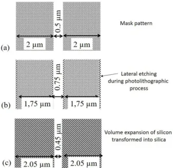
12 The follow up of the etching during the process quite allows to reach the aimed height of the porous silicon core waveguide. Nevertheless, the obtained core waveguide has a rounded shape with a maximum width size of 1.8 µm and a minimum one of 1.7 µm (Figure 5.a) instead of the 2 µm size aimed on the mask pattern.
Thus, due to the smaller width of the waveguides, in the coupling area (Figures 5.b and 5.c), an increase of the distance between the straight and the racetrack waveguide is observed; indeed, a mean gap value of 0.75 µm (Figure 5.c) is obtained compared to the expected 0.5 µm patterned on the mask.
After the complete oxidation step, the height of the waveguide is slightly increased of 0.1 µm as well as its mean width which reaches 2.05 µm (Figure 6.a). The waveguide dimensions which are obtained always allow a single modal propagation of the light (Figure 2).
The width of 2.05 µm for the two waveguides is confirmed by the top view of the coupling region (Figure 6.b). An expansion ratio of about 17% in width reduces consequently the gap: the mean value of the gap is 0.45 ± 0.05 µm (Figure 6.c). Thus the oxidation performed after the photolithographic process reduces the gap by nearly 40%.
13 Figure 6: SEM observations after complete oxidation: (a) Cross section of porous silica waveguide; (b) Top view of the MR with a low magnification; (c) Top view of the coupling area at a higher magnification.
A schema of the width evolution of the waveguide is reported on Figure 7: initially planned on the mask (Figure 7.a), after the photolithographic process (Figure 7.b) and after the complete oxidation (Figure 7.c). Moreover, the width and the height before and after the thermal oxidation as well as the corresponding expansion ratio are reported in Table II for the core and the cladding layers.
14 Figure 7: Schema of the top view of the coupling region of core waveguides reporting the width and the gap between the two waveguides: (a) as planned on the mask, (b) after the photolithographic process and (c) after the complete oxidation step.
Table II: Height and width of the core and cladding layers of the ridge waveguide before and after the complete thermal oxidation and the corresponding expansion ratio.
Core waveguide Before oxidation After oxidation Expansion ratio % Height 0.9 µm 1 µm 11 Width 1.75 µm 2.05 µm 17 Gap 0.75 µm 0.45µm - Cladding waveguide Before oxidation After oxidation Expansion ratio % Height under the core 4.55 µm 4.95 µm 9
Height 3.6 µm 3.9 µm 8 Width under the core 1.75 µm 1.9 µm 9
15 After the photolithographic process, the real separation distance between the two PS waveguides is higher than expected by a mean value of 0.25 µm because of an additional lateral etching that occurred in the core PS layer. This phenomenon had been already observed in a previous study [18].
Then, as already mentioned previously, during the complete oxidation step of PS waveguides, an increase in volume of silicon crystallites occurs [26 - 29]. This volume expansion is due to the transformation of silicon into silica and induces a reduction of the porosity and also an increase of the ridge waveguide dimensions.
In the core waveguide, the increase of the height is about 11% and the one of the width waveguide is of 17%. This width expansion allows to reach a gap of 0.45 µm that is not possible to obtain if, as in our previous study [18], the standard photolithographic process is performed after the oxidation step of the PS layers. The expansion rate values reported in Table II reveal an anisotropic character of the expansion volume all the more marked in the core layer (lower porosity). The photolithography process was initially carried out on straight guides in the same way as the micro-resonators in order to predict the expansion volume. Very similar lateral expansions with less than 0.5% of difference have been obtained showing the reproducible process if it is carried out in a strictly identical way from the elaboration of porous silicon layers to the photolithography process.
This inhomogeneity of the expansion ratio results from the anisotropic porous structure constituted of columnar pore shape, perpendicular to the silicon substrate [35] and typical of the electrochemical etching of P+ orientated (100) silicon substrates. Thus, when the porosity is higher, the width expansion occurs more within the pores inducing a decrease of the pore diameter instead of an increase of the total width. Nevertheless, even with an initial porosity of 80% in the cladding, the width expansion remains significant (9%). So the reduction of the gap with such a core porosity would be also obtained using the method of porous silica waveguide fabrication described in this paper.
16 Then, after having shown the feasibility of reducing the gap in porous silica-based MR, it is important to show that the MRs are optically operational. Using the experimental method described in our previous studies [18], the experimental spectral response of the porous silica MR has been measured and is reported in Figure 8.a.
The transmitted response shows peaks that corresponds to resonance wavelengths. The difference between two resonance wavelengths (Free Spectral Range: FSR) is of 4.35 nm which corresponds to the aimed one considering the effective index and the geometrical parameters of the racetrack cavity.
An extinction ratio of 25 dB has been obtained and corresponds to the contrast between the maximum of transmitted light and the minimal one at resonant wavelengths.
17 Figure 8 : Transmission spectra for one polarization of light of the porous silica racetrack MR : (a) Experimental and calculated spectra (gap of 0.45µm), (b) normalized experimental spectrum (gap of 0.45µm), (c) Calculated spectra for gaps of 0.45 µm and 0.75µm.
Using the equations defined in a previous study on polymers MR [36], the theoretical transmission has been calculated and then adjusted to match the experimental one (Figure 8.a). The adjustment of the resonance shape is performed by modifying the coupling ratio and the propagation losses in the MR with the assumption that the coupling losses are negligible. The wavelength difference, or free spectral range (FSR), is adjusted from the group index [35].
The adjustment of the calculated spectrum to the experimental one has been obtained with a coupling ratio of 30% and a field attenuation constant “a” of 0.86, which corresponds to propagation losses per length unit of 32 dB/cm. To match the experimental FSR, the group index
18 was adjusted to 1.4194. According to Figure 4, a gap of 0.45 – 0.5 µm allows to reach a coupling ratio of about 30 - 40% for the TM mode and for waveguide dimensions of 2 µm x 1 µm. The selected polarization in the experiment presented in Figure 8.a is then the TM mode. As the real dimensions are of 2.05 µm x 0.9 µm, we have calculated again the coupling ratio for these dimension and the same parameters as in figure 4 and verified that a coupling ratio of about 30 % can be obtained for a gap of 0.45 – 0.5 µm.
The corresponding normalized transmission is reported in Figure 8.b. The contrast obtained is nearly of 100% which means that the critical coupling is reached. This demonstrates that the coupling of the light between the access waveguide and the racetrack cavity is optimal as a maximum contrast is obtained. Despite the lateral over lateral etching that occurs due to the porous nature of the layers, this experiment shows clearly that we have succeed in making a ridge porous silica racetrack MR with low gap of about 0.45 – 0.5 µm by taking advantage of the volume expansion of silicon that occurs during oxidation of the ridge PS waveguides. Such gap value allows to reach the critical coupling of around 30% in this case.
If oxidation had been carried out before the photolithographic process, as in our previous study [18], a gap of 0.75 µm instead of 0.45 µm would have been obtained. In this case, the coupling ratio for the same mode (TM) would be 6% (8% for the TE mode). The calculated transmission spectra of the porous silica MR with a gap of 0.75 µm, taking into consideration the same conditions (refractive indices, dimensions, optical losses) except for the coupling ratio shows a lower contrast compared to the transmission spectra of the porous silica MR with a gap of
0.45 µm (Figure 8.c). This comparison clearly demonstrates the interest of reducing the gap.
Without the over lateral etching effect, the gap could be further reduced. If we take into account the reduction obtained of 40%, for a minimum gap before oxidation of 0.5 µm, limited by the resolution of the standard photolithography technique, a gap of 0.3 µm could be obtained after oxidation of the MR. Such a value would further allow to miniaturize the MR by reducing the coupling length and radius of curvature of the MR. It would also allow the use of slightly
19 larger waveguides, respecting the single modal conditions, up to 2.3 µm (width) x 1.5 µm (height) which would induces lower optical losses.
Conclusion
In this paper, a new method of processing racetrack MR based on porous silica ridge waveguides has been demonstrated in the objective to obtain lower gap between the straight access waveguide and the racetrack cavity. The method consists first in performing the standard photolithographic process on PS layers to obtain the ridge PS waveguides and then to carry out their complete oxidation in order to obtain porous silica waveguides. The method adopted previously consisted in oxidizing the PS layers before the processing of the ridge porous silica waveguides. In both method, a lateral etching occurs, reduces significantly the width of the ridge waveguide and increases consequently the gap. Such phenomenon resulted in the use of larger coupling distance (Lc) in the design of the racetrack.
The method demonstrated in this paper allows to use lower coupling distances and so to miniaturize further PS ridge waveguides MRs. To do so, the fabrication process takes advantage of the volume expansion of silicon that occurs during the full oxidation of PS ridge waveguides. The volume expansion is all the more marked when the porosity of the core is low. In this work, we demonstrated a gap reduction of about 40% that has been obtained due to the expansion phenomena with an initial porosity of 50%. The resulting porosity after oxidation (20 %) remains sufficient for sensor application for gases or small molecules as proteins which can be easily grafted on porous silica after an appropriate functionalization of its high specific surface.
ACKNOWLEDGMENTS
This work is supported by the BIOCAP project, the ANR MIDVOC funded by the French Research Ministry, and the ARED funded by the Conseil Départemental des Côtes d’Armor and the Région Bretagne. The authors thank the CCLO (Centre Commun Lannionnais d’Optique) platform for its technical support in this work.
20
REFERENCES
[1]. V. Torres-Costa, R. J. Martın-Palma, “Application of nanostructured porous silicon in the field of optics. A review”, J Mater. Sci. 45 (2010) pp. 452823–2838. doi: 10.1007/s10853-010-4251-8.
[2] O. Bisi , S. Ossicini, L. Pavesi, “Porous silicon: a quantum sponge structure for silicon based optoelectronics” , Surf. Sci. Rep., 264, (2000) pp. 1-126. doi.org/10.1016/S0167-5729(99)00012-6.
[3] S Dhanekar, I Sharma, SS Islam, “Optical measurement of trace level water vapours using functionalized porous silicon: selectivity studies, RSC Advances 6 (76), (2016) pp. 72371-72377. doi : 10.1039/C6RA12669C.
[4] T. Jalkanen, V. Torres-Costa, J. Salonen, M. Björkqvist, E. Mäkilä,, J. M. Martınez, Duart,V-P Lehto, “Optical gas sensing properties of thermally hydrocarbonized porous silicon Bragg reflectors.”, Opt Exp 17 (7) (2009) pp. 5446-5456. doi.org/10.1364/OE.17.005446.
[5] S. Chan, P.M. Fauchet, Y. Li, LJ. Roberg, BL. Miller, “Porous silicon microcavities for biosensing applications”, Phys. Status Solidi A- Appl. Res. 182, (2000) pp. 541- 546. doi.org/10.1002/1521-396X(200011)182:1<541::AID-PSSA541>3.0.CO;2-#
[6] S. Dhanekar, S. Jain, “Porous silicon biosensor: Current status”, Biosensors and bioelectronics 41, (2013) pp. 54-64. doi.org/10.1016/j.bios.2012.09.045
[7] V. Lehmann, R. Stengl, A. Luigart, “On the morphology and the electrochemical formation mechanismof mesoporous silicon”, Materials Science and Engineering B69–70 (2000) pp. 11–
22. doi.org/10.1016/S0921-5107(99)00286-X.
[8] E. Lorenzo, C. J. Oton, N. E. Capuj, M. Ghulinyan, D. Navarro-Urrios, Z. Gaburro, and L. Pavesi, "Porous silicon-based rugate filters," Appl. Opt. 44, 5415-5421 (2005). doi.org/10.1364/AO.44.005415.
[9] S. Ilyas, J. Böcking, K. Kilian, PJ. Reece, J. Gooding, K. Gaus, M. Gal, “Porous silicon based narrow line-width rugate filters”, Optical Materials 29, (2007) pp. 619-622. doi.org/10.1016/j.optmat.2005.10.012.
[10] I. Rea, M. Iodice, G. Coppola, I. Rendina, A. Marino, L.D. Stefano, “A porous silicon-based Bragg grating waveguide sensor for chemical monitoring”, Sens. Actuators B: chem. 139, n°1, (2009) pp. 39-43. doi:10.1016/j.snb.2008.08.035.
21 [11] Weiss S.M., Wei X. “Porous Silicon Optical Waveguides”. In: Canham L. (eds) Handbook of Porous Silicon. Springer, Cham (2017) pp. 1-8. doi.org/10.1007/978-3-319-04508-5_83-2. [12] S. M. Weiss, G. Rong, JL. Lawrie, “Current status and outlook for silicon-based optical biosensors”, Physica E 41, (2009) pp. 1071-1075. https://doi.org/10.1016/j.physe.2008.08.031.
[13] C.Y. Chao, W. Fung, L.J. Guo, “Design and Optimization of Microring Resonators in Biochemical Sensing Applications”, Journal of Lightwave Technology 24, n°3, (2006) 1395-1402. doi: 10.1109/JLT.2005.863333.
[14] C. Ciminelli, F. Dell’Olio, C. E. Campanella, M. N. Armenise, “Labelfree optical resonant sensors for biochemical applications”, Progress in Quantum Electronics, 37 (2013) p. 51-107. doi.org/10.1016/j.pquantelec.2013.02.001.
[15] C. Ciminelli, F. Dell’Olio, D. Conteduca, C. M. Campanella et M. N. Armenise, “High performance SOI microring resonator for biochemical sensing”, Optics and Laser Technology, 59 (2014) p. 60 - 67. doi.org/10.1016/j.optlastec.2013.12.011.
[16] T. Hutter, N. Bamiedakis, S. R. Elliott, “Theoretical Study of Porous Silicon Waveguides and Their Applicability for Vapour Sensing”, Proceedings of COMSOL Conference, (2010) Paris.
[17] G.A Rodriguez, H. Shuren, S.M. Weiss, “Porous silicon ring resonator for compact, high sensitivity biosensing applications”, Optics Express 23, n° 6 (2015). pp. 7111-7119. doi.org/10.1364/OE.23.007111.
[18] P. Girault, N. Lorrain, J. Lemaitre, L. Poffo, M. Guendouz, I. Hardy M. Gadonna A. Gutierrez, L. Bodiou, J. Charrier “Racetrack micro-resonators based on ridge waveguides made of porous silica”, Optical Materials, 50 (2015) pp. 167-174, doi.org/10.1016/j.optmat.2015.10.017.
[19] R. Caroselli, S. Ponce-Alcantara, F. Prats Quilez, D. Martin Sanchez, L. Torrijos Moran, A. Griol Barres, L. Bellières, H. Bandarenka, K. Girel, V. Bondarenko, J. Garcia-Ruperez, “Experimental study of the sensitivity of an porous silicon ring resonator sensor using continuous in-flow measurements”, Optics Express, Vol. 25, (2017) pp. 31651-31659. doi.org/10.1364/OE.25.031651.
[20] P. Azuelos, P. Girault, N. Lorrain, L. Poffo, I. Hardy, M. Guendouz, M. Thual, Theoretical investigation of Vernier effect based sensors with hybrid porous silicon-polymer optical waveguides, Journal of Applied Physics 121 (2017) pp.144501-144521. https://doi.org/10.1063/1.4980010.
22 [21] R. Landgraf, R. Kirchner, A. Finn, S. Arndt, T. Haugwitz, F. Deicke, W.J. Fischer, “Polymer Microring Resonator Directly Patterned by Multilevel-Nanoimprint: Integration into Biosensor System with a Miniaturized Microfluidic System” GMA/ITG-Fachtagung Sensoren und Messsysteme, Nürnberg 2012 Tagungsband (2012) pp. 259–267.
doi:10.5162/sensoren2012/2.4.2.
[22] D. Dai, B. Yang, L. Yang, Z. Sheng, and S. He, “Compact Microracetrack Resonator Devices
Based on Small SU-8 Polymer Strip Waveguides”, IEEE photonics technology letters, vol.21, 4 (2009) pp. 254-256. doi:10.1109/LPT.2008.2010555.
[23] A. Maalouf, M. Gadonna, D. Bosc, “An improvement in standard photolithography resolution based on Kirchhoff diffraction studies”, Journal of Physics D: Appl. Phys. 42, (2009) pp. 015106-015117. doi.org/10.1088/0022-3727/42/1/015106.
[24] P. Ferrand and R. Romestain, “Optical losses in porous silicon waveguides in the near-infrared: Effects of scattering” Applied Physics Letters 77, (2000) pp. 3535-3537. doi.org/10.1063/1.1329161.
[25] J. Charrier, C. Lupy, L. Haji, C. Boisrobert, “Optical study of porous silicon buried waveguides fabricated from p-type silicon”, Materials Science in Semiconductor Processing 3, (2000) pp.357-361. doi.org/10.1016/S1369-8001(00)00056-1.
[26] E. V. Astrova, V. A. Tolmachev, “Effective refractive index and composition of oxidized porous silicon films”, Materials Science and Engineering B 69 (2000) pp. 142-148. doi.org/10.1016/S0921-5107(99)00236-6.
[27] G. Toth, K. Kordas, A. E. Pap, J. Vähäkangas, A. Uusimäki, S. Leppävuori, “Origin
and FEM-assisted evaluation of residual stress in thermally oxidized porous silicon”, Computational Materials Science 34 (2005) pp. 123–128. doi:10.1016/j.commatsci.2004.12.071.
[28] A. E. Pap, K. Kordás, G. Tóth, J. Levoska, A. Uusimäki et al. “Thermal oxidation of porous silicon: Study on structure”, Appl. Phys. Lett. 86, 041501 (2005).doi: 10.1063/1.1853519.
[29] P. Pirastesh, J. Charrier, A. Soltani, S. Haesaert, L. Haji, C. Godon, N. Errien, “The effect of oxidation on physical properties of porous silicon layers for optical applications”, Applied Surface Science, 253 (2006) pp. 1999-2002. doi.org/10.1016/j.apsusc.2006.03.083.
[30] N. Lorrain, M. Hiraoui, M. Guendouz, L. Haji, “Functionalization control of porous silicon optical structures using reflectance spectra modeling for bio sensing applications”, Material Science and Engineering B 176, (2011) pp. 1047-1053. doi.org/10.1016/j.mseb.2011.05.040.
[31] M. Hiraoui, L. Haji, M. Guendouz, N. Lorrain, A. Moadhen and O. Oueslati, “Towards a biosensor based on anti-resonant reflecting optical waveguide fabricated from porous silicon”, Biosensors and Bioelectronics 36 (2012) pp. 212-216. doi.org/10.1016/j.bios.2012.04.022.
23 [32] P. Girault, P. Azuelos, N. Lorrain, L. Poffo, J. Lemaitre, P. Pirasteh, I. Hardy, M. Thiual, M. Guendouz and J. Charrier, “Porous silicon micro-resonator implemented by standard photolithography process for sensing application”, Optical Materials, 72 (2017) pp. 596 – 601. doi.org/10.1016/j.optmat.2017.07.005.
[33] J. W. Westerveld, S. M. Leinders, K. W.A. van Dongen, H. P. Urbach, and M. Yousefi, ”Extension of Marcatili’s analytical approach for rectangular silicon optical waveguides”, J. of Lightwave Technology, vol. 30, 14 (2012). doi:10.1109/JLT.2012.2199464).
[34] K. Okamoto, “Fundamentals of optical waveguides”, 2nd edition, Academic Press, (2006). p. 197-198 and pp. 37-40.
[35] V. Lehmann, U. Gösele, “On the morphology and the electrochemical formation mechanism of mesoporous silicon”, Materials Science and Engineering B69-70 (2000) pp. 11-22. doi.org/10.1016/S0921-5107(99)00286-X.
[36] P. Girault, N. Lorrain, L. Poffo, M. Guendouz, J. Lemaitre, C. Carré, M. Gadonna, D. Bosc, G. Vignaud, “Racetrack micro-resonators based on ridge waveguides made of porous silica ”, J. Appl. Phys. 117 (2015) pp. 104504-1–104504-8. doi.org/10.1016/j.optmat.2015.10.017.