HAL Id: hal-01131545
https://hal.archives-ouvertes.fr/hal-01131545
Submitted on 13 Mar 2015
HAL is a multi-disciplinary open access
archive for the deposit and dissemination of
sci-entific research documents, whether they are
pub-lished or not. The documents may come from
teaching and research institutions in France or
abroad, or from public or private research centers.
L’archive ouverte pluridisciplinaire HAL, est
destinée au dépôt et à la diffusion de documents
scientifiques de niveau recherche, publiés ou non,
émanant des établissements d’enseignement et de
recherche français ou étrangers, des laboratoires
publics ou privés.
High efficiency low power rectifier design using zero bias
schottky diodes
Aya Mabrouki, Mohamed Latrach, Vincent Lorrain
To cite this version:
Aya Mabrouki, Mohamed Latrach, Vincent Lorrain. High efficiency low power rectifier design using
zero bias schottky diodes. FTFC, May 2014, Monaco, France. �10.1109/FTFC.2014.6828604�.
�hal-01131545�
High Efficiency Low Power Rectifier Design using
Zero Bias Schottky Diodes
Aya MABROUKI
ESEO, 10 Bd Jeanneteau, 40107 Angers IETR, 20 Avenue des Buttes de Coësmes CS 70839 F - 35708 Rennes Cedex 7
Mohamed LATRACH, Vincent LORRAIN
ESEO, 10 Bd Jeanneteau, 40107 Angers IETR, 20 Avenue des Buttes de CoësmesCS 70839 F - 35708 Rennes Cedex 7 [email protected]
Abstract—In this paper we present the design of high
efficiency low power rectifier for microwave energy harvesting. The proposed circuit is based on a voltage booster formed by a voltage doubler type Latour structure. The circuit topology including parasitic elements and microstrip lines has been studied and optimized for high efficiency energy conversion dedicated to low input power operations (below -10dBm). Measurement results show 21% and 38% RF-DC conversion efficiencies for, respectively, -20dBm and -10dBm input power for 10KΩ resistor load at 850MHz. Experimental performances
of the rectifier are in good agreement with the simulated ones.
Keywords—Schottky, rectenna, energy harvesting
I. INTRODUCTION
The widespread diffusion of remotely powered devices has led to a growing interest in wireless energy harvesting techniques. This concept can be used to supply low power electronic devices like sensors or RFID tags over distances of several meters [1]. One approach of wireless power transmission uses the electromagnetic (EM) waves and energy transfer process can be described by three main stages. First, the power signal is generated and sent by an emitting antenna. Then, it is transported under the form of a free propogating EM wave towards the receiver where it is collected by the rectenna (rectifying antenna) to be transformed into a DC power. Rectenna efficiency optimization is still a hard task for RF designers when the incident power levels are very low [1][2]. Several rectification structures have been proposed to improve the RF-DC power conversion efficiency. In [3], [4], and [5] harmonic terminations, employed in RF power amplifier (PA) designs, have been used to improve the efficiency of a single stage shunt diode rectifier. However, optimized results are obtained only for input power beyond 0dBm. Other research works, [6][7][8], deal with the improvement of the DC output filter of the rectenna to boost the DC voltage and the conversion efficiency but they still not very efficient for low power detection. The conventional rectifying structures that have been widely studied, measured, and discussed are mainly single shunt and series mounted diode, voltage doubler and bridge rectifiers. In this work, we propose a voltage doubler structure type Latour, which to the author knowledge, has not been previously used in rectenna design. The paper is organised as follows: First, we review the different rectifying
topologies. Then, we present the proposed circuit and its characteristics. In section III, we give the design guidelines and the simulated results. Finally, the measurement results are shown and discussed in section IV.
II. RECTENNA CONFIGURATIONS
A. Conventional rectifier structures
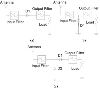
Rectifier circuits are built around diodes or diodes mounted transistors. In Fig. 1 we present three conventional rectifying structures the most used in litterature [8] [9]. The circuit is generally composed of 4 blocks: The input filter to preserve the antenna re-irradiating the high order harmonics generated by the rectifier, the input matching network (not presented in Fig. 1), the rectifying diode, and the output DC filter to filter harmonics in order to reduce voltage and current overlap. Diodes threshold voltage is a key factor when designing the rectenna. In fact, under high power levels, diode threshold is not important since it is very low compared to incident high frequency voltage amplitude. However, it becomes critical for low incident power levels due to losses. In this work, we use a zero bias shottky diode HSMS2852 with low threshold voltage of 150mV and a low junction capacitance Cj0 of 0.18pF.
(a) (b)
(c)
Fig. 1. Conventional rectenna topologies: (a) series; (b) shunt; (c) single stage voltage doubler
The main characteristics that should be optimized when designing rectennas are the DC output voltage Vout and the
RF-DC power conversion efficiency defined as [10]:
2 2 2 . . . 4 .
λ
π
η
G E Z R V P P air L out RFin DCout = = (1) Where RL is the load resistance, Zair is air characteristicimpedance (120π ohms), E is electric field RMS value at receiver position, G is the receiving antenna gain, and λ is the wavelength.
RF designers should find a trade-off between a high output voltage and good power conversion efficiency when choosing the rectifier structure. A comparison between the performance of conventional rectifier topologies shown in Fig. 1, as a function of input power, has been widely discussed in several works. [10] used a Rectenna Figure of Merit (RFoM), described in (2), to compare the different rectifying topologies performances. d optimalLoa uit DCopencirc in
V
P
RFoM
(
)
=
.
η
(2) It reported that series mounted diode rectifier seems to have the highest RFoM for low input power (below -5dBm) and offers a best compromise between DC output level and power conversion efficiency.B. The Proposed rectifier topology
The rectifier topology we propose in this work is depicted in Fig. 2 (a). It is based on a voltage booster formed by a voltage doubler type « Latour ». The circuit includes two capacitors C1 and C2 and two rectifier diodes D1 and D2. The voltage source supplies two separate branches in parallel. A first branch is constituted by the series connection of the diode D1 and the capacitor C1, and the second branch is constituted by the diode D2 and the capacitor C2 in series, one terminal of the capacitor C1 being connected to one terminal of the capacitor C2. One capacitor is charged at the positive half wave and the other at the negative half wave. The output voltage Uout is collected at the terminals of the circuit formed by the two capacitors C1 and C2. D1 D2 C1 C2 Uout Uin V1 V2
Positive half wave
Negative half wave
(a)
(b)
Fig. 2. (a) The proposed rectifier topology: “Latour” doubler; (b) the corresponding input and output waveforms
For open circuit case, the output voltage is twice the input peak voltage. The input and output waveforms of the circuit are illustrated in Fig. 2(b). This structure will be studied and optimized to design a high efficiency low power rectifier at 915MHz.
III. DESIGN GUIDELINES AND SIMULATION RESULTS
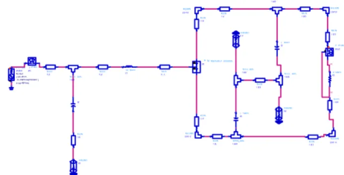
The global circuit optimization technique should take into account several factors such as passive components dimension including Q factor and tolerance, mircostrip lines added for matching and the non-linear behavior of the diode. These opimizations were made using the software ADS (Momentum EM simulations) from Agilent Technologies.
A. Circuit Design
The circuit architecture including passive components and microstrip lines is described in Fig. 3. An input inductance and a shunt capacitor of 3 pF have been added to improve the input matching. Special attention should be given to the choice of passive component in order to reduce the effect of dispersion on the sensitivity of the circuit. The input inductance has a value of 39nH and a Q factor of 35 at 800MHz. The output capacitors C1 and C2 are equals to 100pF. The proposed
structure is designed on 1.6mm thickness FR4 substrate (εr=4.5 and tanδ=0.025).
Fig. 3. Global circuit topology
B. Simulation results
The circuit has been simulated under Harmonic balance (HB) routine from Agilent ADS. S-paramter simulations have been caried out to optimize the matching network of the rectifier to a 50Ω input impedance at 915MHz (for input power below -10dBm). The simulated input return loss is illustrated in Fig. 4 and -19dB S11 is obtained at 915MHz.
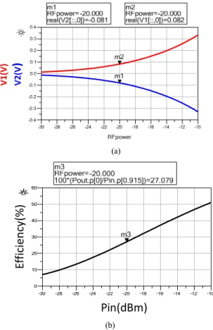
Harmonic balance sweep simulations have been carried out to determine the best compromise between high output DC voltage and high power conversion efficiency. Different load resistors have been tested to determine the optimal load. The output voltage achieved for a DC optimal load of 10KΩ for different input power and the corresponding RF-DC conversion efficiency are plotted respectively in Fig. 5(a) and (b) at 915MHz. V1 (V ) V2 (V
)
(a)Ef
fi
ci
en
cy
(%
)
Pin(dBm)
(b)Fig. 5. (a) Output DC voltage; (b) RF-DC conversion efficiency
As can be seen, 0.163 V and 27% RF-DC conversion efficiency are obtained at -20dBm input power. At -10dBm almost 50% efficiency can be achieved.
IV. RECTIFIER MEASUREMENT RESULTS
The rectifier has been designed and printed on a FR4 substrate. A photograph of the circuit is given in Fig. 6. The circuit occupies a total area of 5cm² which still very small in comparison with the area of rectifier structures using microstrip stub lines either in output or input filters [6] [9].
Fig. 6. Photograph of the rectifier
The measured input return loss S11 is shown in Fig. 7. The rectifier is slightly shifted but it is well matched with -13dB S11 at 850MHz for 10KΩ resistor load.
0.5 1.0 1.5 0.0 2.0 -15 -10 -5 -20 0 freq, GHz d B (S (1 ,1 )) Fig. 7. Measured S11
The measurement setup, used to characterize the circuit, is described in Fig. 8. The directional coupler monitors the second harmonic power level. The power meter is used to measure the reflected power. The DC output voltage Vout is
obtained by subtracting the voltage V- from voltage V+ .
rectifier Power meter Rload Directional coupler Coax Isolator RF source V+ V
-Fig. 8. Measurement setup of the rectifier
We measured the output DC voltage at three different input power levels (-20dBm, -15dBm, -10dBm) for 10 KΩ resistor load and we plotted it as a function of frequency in Fig. 9. Maximum DC voltages of 144mV and 610mV are obtained at 850MHz for -20dBm and -10dBm respectively. Good correlation with simulation results is observed at -20dBm and -15dBm input powers.
0 0,1 0,2 0,3 0,4 0,5 0,6 0,7 700 800 900 1000 Vo u t( V ) Freq(MHz) RL=10KOhms Pin=-20dBm Pin=-15dBm Pin=-10dBm
Fig. 9. Measured DC output voltage as a function of frequency
The power conversion efficiency has been computed according to (3) and plotted as a function of frequency in Fig. 10. A 21% maximum power conversion efficiency is measured at 850MHz for -20dBm input power and 10KΩ resistor load. The circuit performances are in good agreement with the predicted simulted results for input power below -15dBm. At -10dBm input power, measured power conversion
efficiency is reduced of 13% in comparison with the simulated one due to ohmic losses of the diodes.
inc L out inc outDC rec
P
R
V
P
P
*
2=
=
η
(3) Where Pinc is the incident RF power, RL is the DC load and Voutis the output DC voltage.
0 5 10 15 20 25 30 35 40 45 700 800 900 1000 Ef fi cie n cy (%) Freq(MHz) RL=10KOhms Pin=-20dBm Pin=-15dBm Pin=-10dBm
Fig. 10. Measured efficiency as a function of frequency
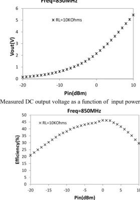
Measurement of the rectifier performances as a function of input power have been also carried out and plotted in Fig. 11 and Fig.12. 610mV and 1.17V DC output voltages are measured respectively at -10dBm and -5dBm input powers and 46% maximum RF-DC conversion efficiency is achieved at 0dBm input power. 0 1 2 3 4 5 6 -20 -10 0 10 V o ut (V ) Pin(dBm) Freq=850MHz RL=10KOhms
Fig. 11. Measured DC output voltage as a function of input power
0 5 10 15 20 25 30 35 40 45 50 -20 -15 -10 -5 0 5 10 Effi ci en cy (% ) Pin(dBm) Freq=850MHz RL=10KOhms
Fig. 12. Measured conversion efficiency as a function of input power
The proposed rectifier presents good performances for low power detection in comparison with the state of the art [10]. Most of the reported researches in rectifier designs operate at 2.4GHz. In [10], 300mV DC output voltage is obtained at 2.45GHz for -15dBm input power and 6KΩ resistor load.
V. CONCLUSION
A voltage doubler rectifier, type Latour, has been proposed and measured. The circuit is dedicated to low power detection applications at 850MHz. The experimental results validated the circuit high efficiency operation at low input power (below -10dBm). 21% RF-DC conversion efficiency is achieved at 850 MHz for -20dBm input power and 10KΩ resistor load. Future works involve the increase of the voltage doubler stages to boost the output DC voltage and improve the power conversion efficiency.
REFERENCES
[1] C. Mikeka, H. Arai, “Design issues in Radio Frequency Energy harvesting System,” Sustainable Energy Harvesting Technologies –Past, Present and Future, pp. 235-256, Dec 2011.
[2] A. Dolgov, R. Zane, and Z. Popovic, “Power management system for online low power rf energy harvesting optimization,” Circuits and Systems I: Regular Papers, IEEE Transactions on, vol. 57, no. 7, pp. 1802–1811, 2010.
[3] S. Imai et. al., “Efficiency and harmonics generation in microwave to dc conversion circuits of half-wave and full-wave rectifier types,” in 2011 IEEE MTT-S International, May 2011, pp. 15 –18.
[4] M. Roberg, T. Reveyrand, I. Ramos, E. A. Falkenstein, Z. papović, “High-Efficiency Harmonically Terminated Diode and Transistor Rectifiers,” IEEE Transactions on Microwave Theory and Techniques, vol. 60, No. 12 December 2012, pp. 4043-4052.
[5] Falkenstein, E., M. Roberg, and Z. Popovic, “Low-power wireless power delivery,” IEEE Trans. Microw. Theory and Tech., Vol. 60, No. 7, pp. 2277-2286, Jul. 2012.
[6] A. Mabrouki, M. Latrach, Z. Sayegh, “Design and experiment of RF rectifiers for wireless power transmission,” 13th Mediterranean
Microwave Symposium, Sep 2013, pp. 1-4.
[7] H. Takhedmit et. al., “A 2.45-ghz low cost and efficient rectenna,” in 2011 Proceedings of the Fourth European Conference in Antennas and Propagation (EuCAP), April 2011, pp. 1-5.
[8] J. Zbitou, M. Latrach, S. Toutain, “Hybrid Rectenna and monolithic integrated zero bias microwave rectifier,” Microwave theory and techniques, IEEE transactions on, vol. 54, no. 1, pp. 147-152, Jan 2006. [9] A. Douyère, F. Alicalapa, and J-D. Lan Sun Luk, “high efficiency
microwave rectenna circuit: Modeling and design,” Electronic Letters, vol. 44, pp. 1409-1410, 2008.
[10] V. Marian, C. Menudier, M. Thevenot, C. Vollaire, J. Verdier, B.Allard, “Efficient design of rectifying antennas for low power detection ,” 2011 MTT –S International Microwave Symposium Digest, June 2011, pp 1-4.