HAL Id: hal-01112963
https://hal.archives-ouvertes.fr/hal-01112963
Submitted on 4 Feb 2015
HAL is a multi-disciplinary open access
archive for the deposit and dissemination of
sci-entific research documents, whether they are
pub-lished or not. The documents may come from
teaching and research institutions in France or
abroad, or from public or private research centers.
L’archive ouverte pluridisciplinaire HAL, est
destinée au dépôt et à la diffusion de documents
scientifiques de niveau recherche, publiés ou non,
émanant des établissements d’enseignement et de
recherche français ou étrangers, des laboratoires
publics ou privés.
Substrate bonding using electroplated copper through
silicon vias for VCSEL fabrication
Fethallah Taleb, Christophe Levallois, Cyril Paranthoen, Nicolas Chevalier,
Olivier de Sagazan, Antoine Letoublon, Olivier Durand
To cite this version:
Fethallah Taleb, Christophe Levallois, Cyril Paranthoen, Nicolas Chevalier, Olivier de Sagazan, et al..
Substrate bonding using electroplated copper through silicon vias for VCSEL fabrication. 26th
Inter-national Conference on Indium Phosphide and Related Materials (IPRM 2014), May 2014, Montpellier,
France. IEEE, Indium Phosphide and Related Materials Proceedings (IPRM 2014), 26th International
Conference on, pp.P21, 2014, �10.1109/ICIPRM.2014.6880543�. �hal-01112963�
Substrate bonding using electroplated copper through
silicon vias for VCSEL fabrication
F. Taleb
1, C. Levallois
1, C. Paranthoen
1, N. Chevalier
1, O. De Sagazan
2, A. Letoublon
1, and O. Durand
11
: Université Européenne de Bretagne, France INSA, CNRS UMR 6082 FOTON, F-35708 Rennes, France
2
: GM-IETR UMR-CNRS 6164, Université de Rennes1,F-35042 Rennes Cedex, France e-mail: [email protected]
Short-Abstract—We present a novel approach to bound any substrate on a silicon host platform, in the particular case of the realization of InP based vertical cavity surface emitting lasers (VCSEL). This process is based on a mechanical bonding, using electroplated copper through silicon vias. It enables a cost effective bonding with a low induced stress, and a significant improvement of the device thermal properties. Preliminary results are presented on the realization of light emitting diodes.
I. INTRODUCTION
Vertical bonding of substrate is becoming more and more used in microelectronics to proceed to a 3D integration in combination with TSV (Through Silicon Vias) interconnexions Also for photonic applications, bonding is interesting to proceed to III-V components hybrid integration on mature silicon platform. It enables to benefit on the same chip electronics, lasers, modulators, and waveguides, with the use of adhesive polymer bonding [1] or a Vand der Waals bonding [2]. Also, to improve device performances, III-V components are commonly bonded on host substrates presenting a high thermal resistivity. In the case of such demanding devices such as Vertical (external) cavity surface emitting lasers (V(E)CSEL), metallic bonding on a diamond substrate, and on metallic substrates have been reported to drastically improve their performances [3-6]. Nevertheless, in this last case, the integration with silicon microelectronics is unfortunately not possible. Also, in the case of bonding on metallic copper substrate, which is already compatible with microelectronic processing and also present undoubtedly cost effective interests, it is well known that thick copper layers may induce stress within the wafers related to the difference in the thermal coefficient expansion [7], which may hinder any post bonding processing. In this paper, we propose a novel bonding process of photonic devices, combining the high potential of silicon for microelectronics, and thermal interests of copper. This process is applied to bond individual 1.55 µm emitting VCSEL chip, and preliminary results are presented and discussed.
II. FABRICATION PROCESS DESCRIPTION
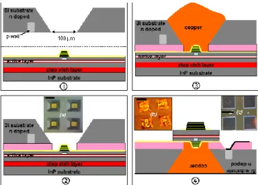
In the following we present the bonding process, we called TSHEC bonding, for Trough Silicon Holes Electroplated Copper bonding. TSHEC process flow is described on the Fig.1, in the case of the realization of a VCSEL device. It begins with the preparation of the two substrates to be bonded (step ). On one hand, on the host n doped (001) silicon substrate, a micrometer thick SiO2 layer is firstly realized by
wet oxidation. It is used as a mask layer to realize 100 µm square holes based on the TMAH anisotropic wet etching. As a simple demonstration of Si microelectronics integration, we insert on silicon a pn junction temperature sensor, by introducing P-wells realized by thermal diffusion on one side of the substrate. On the other hand, the substrate to be bonded is also processed. It firstly consists in the growth by gas source molecular beam epitaxy on n doped (001) InP substrate, of the InGaAs stop etch layer, the active layer (strained quantum wells), a type II buried tunnel junction (BTJ) (GaAsSb:p+, InGaAs:n+), the whole being sandwiched between n doped InP layers. Four periods of dielectric DBR (aSi/aSiN) is deposited by RF sputtering, followed by dry etching to keep a 15 µm in diameter DBR above the BTJ. The n contact (Ni/GeAu/Ni/Au) is then evaporated on the whole sample.
In the next step, both substrate are slightly bonded using an adhesive layer (step ). BCB is first spinned onto the InP susbtrate, followed by a soft thermal baking. Then, on a conventional UV aligner, DBR mesas are centered within the holes in the silicon substrate, slightly pressed onto each other, and baked at 250°C to finalize the BCB curing. At this stage, the BCB layer above the DBR mesa is removed by dry etching, passing by the holes in the silicon substrates, revealing the metallic n contact layer, as shown on insert (a).
Figure 1 : TSHEC bonding process flow description : Si and InP substrates preparation (step ), pre-bonding of both substrates (step ), bonding with
copper filling of the holes (step ), InP based VCSEL and Si based temperature sensor device realizations (step ). Inserts present pictures at different step of the process, after pre-bonding (a), copper holes filling (b) and
This BCB layer is removed, to enable in the next step a close proximity between the bonded device, and the copper layer, which acts as a thermal heat sink.
The third step (step ) consists in filling the holes via with electroplated copper. The equipotential contact to initiate the copper electroplating is taken on the n contact layer on the InP substrate. The copper layer will thus start growing from this layer in the bottom of the holes. The copper layer thickness gradually increases, till it fills out completely the holes. Thanks to the splayed profile of the Si holes, this copper layer ensures the mechanical bonding of the InP substrate onto the silicon, like a clamp will do.
In the last step of the process (step ), a mechanical polishing is performed on the silicon side to remove the excess copper. As shown on insert (b), the holes are completely filled out with copper. Also, the InP substrate is removed by mechanical and chemical etching. The remaining InP based micrometer thick layer is then processed to define individual VCSEL dies (400*400 µm²), as shown on the insert (b). VCSEL process is finalized after the realization of a 100 µm in diameter top dielectric DBR (four pairs), and the deposition of the top n contact layer on the InP side. Aluminum is finally deposited on both sides to realize the ground contact on the backside of the silicon substrate, as well as the temperature sensor top contact.
III. CHARACTERIZATIONS
High resolution x-ray diffraction spectra of 2θ/ω mode scans were performed on sample to investigate the crystal line quality, and the stress potentially induced by the bonding procedure. Related to the large x-ray spot (7 mm long, and 1 mm wide), the measurement has been performed on an average number of 5-6 bonded dies. The measured diffraction spectrum is shown on Fig.2. The silicon diffraction peak is clearly identified at 69.127°. The lowest peak at 63.33° exactly matches with the diffraction of pure relaxed InP. We can thus deduce that TSHEC bonding process induces very low stress on the bonded sample. In comparison with an InP substrate, the diffraction peak width is slightly increased by a factor of 4, and may come from slight tilts of InP dies. Further experiments are necessary to clarify its origin.
Figure 2 : X-ray diffraction (ω-2θ) measured on TSHEC bonded InP dies. Insert is the picture of the sample.
. 1,0 1,1 1,2 1,3 1,4 1,5 1,6 0 5 10 15 20 25 30 -3 -2 -1 0 1 2 3 4 5 6 V o lta g e ( V ) Current (mA) In te g ra te d P o w e r (a . u .) In te n s it y (a rb . u n it ) W avelength (µm ) 2m A 10 m A 30 m A
Figure 3 : Electroluminescence spectra of InP TSHEC bonded LEDs. Insert are the I(V) and L(I) characteristics.
Finally, LEDs devices have been fully processed as a preliminary step of the validation of the TSHEC process. In this case, the active layer consists in 1.45 µm emitting quantum dashes on InP. Fig. 3 shows spectrum at function of several injected currents. In the investigated current range, emitted wavelength is centred at 1.45 µm, and there is no evidence of any wavelength shift related to thermal heating of the LED.
IV. CONCLUSION
We described of novel process to bond VCSELs on silicon substrate, combining an efficient heat spreading canal, and silicon functionalities. Preliminary results have been presented, indicating a stress free bonding, and an efficient thermal dissipation. Experiments are on duty to perform the TSHEC process on VCSEL devices.
REFERENCES
[1] M. Lamponi, S. Keyvaninia, C. Jany, F. Poingt, F. Lelarge, G. de Valicourt, G. Roelkens, D. Van Thourhout,S. Messaoudene, J.-M. Fedeli, and G. H. Duan, “Low-Threshold Heterogeneously Integrated InP/SOI Lasers With a Double Adiabatic Taper Coupler”, IEEE Photon. Technol. Lett. Vol. 24, 1, pp76, 2012
[2] J. Van Campenhout, P. Rojo Romeo, P. Regreny, C. Seassal, D. Van Thourhout, S. Verstuyft, L. Di Cioccio, J.-M. Fedeli, C. Lagahe, and R. Baets, “Electrically pumped InP-based microdisk lasers integrated with a nanophotonic silicon-on-insulator waveguide circuit,” Opt. Express vol 15, 11, pp 6744, (2007)
[3] Z. Zhao, S. Bouchoule, J. Y. Song, E. Galopin, J.-C. Harmand, J.Decobert, G. Aubin, and J.-L. Oudar, “Subpicosecond pulse generationfrom a 1.56 m mode-locked VECSEL,”Opt. Lett., vol. 36, no. 22, pp.4377–4379, 2011
[4] S. Jatta, B. Koegel, M. Maute, K. Zogal, F. Riemenschneider, G. Bohm, M.-C. Amann, and P. Meissner, “Bulk-Micromachined VCSEL At 1.55µm With 76-nm Single-Mode Continuous Tuning Range,” IEEE Photon. Tech-nol. Lett. 21, 1822–1824 (2009)
[5] Z. Zhao, S. Bouchoule, L. Ferlazzo, A. Sirbu, A. Mereuta, E. Kapon, E. Galopin, J-C. Harmand, J. Décobert, and J-L. Oudar, “Cost-Effective Thermally-Managed 1.55- mVECSEL With Hybrid Mirror on Copper Substrate”, IEEE Journ. of Quant Electron., vol 48, n° 5, pp 643, 2012 [6] F. Taleb, C. Levallois, C. Paranthoën, J-P Gauthier, N. Chevalier, M.
Perrin, Y. Léger, O.De Sagazan, and A. Le Corre, “VCSEL Based on InAs Quantum-Dashes With aLasing Operation Over a 117-nm Wavelength Span”, IEEE Photon. Technol. Lett., vol 25, n° 21, pp 2126-2129, 2013.
[7] P. N. An and P. A. Kohl, “Thermal-Mechanical Stress Modeling of Copper Chip-to-Substrate Pillar Connections”, IEEE , Trans. Compon. Packag, Technol. vol. 33, n°. 3,pp 621-628, 2010.