HAL Id: tel-02946263
https://tel.archives-ouvertes.fr/tel-02946263
Submitted on 23 Sep 2020HAL is a multi-disciplinary open access archive for the deposit and dissemination of sci-entific research documents, whether they are pub-lished or not. The documents may come from teaching and research institutions in France or abroad, or from public or private research centers.
L’archive ouverte pluridisciplinaire HAL, est destinée au dépôt et à la diffusion de documents scientifiques de niveau recherche, publiés ou non, émanant des établissements d’enseignement et de recherche français ou étrangers, des laboratoires publics ou privés.
molecule-driven assembly
Yesica Flores
To cite this version:
Yesica Flores. Hybrid semiconducting nanoplatelets : synthesis and molecule-driven assembly. Coor-dination chemistry. Sorbonne Université, 2018. English. �NNT : 2018SORUS464�. �tel-02946263�
Sorbonne Université
Ecole doctorale de Chimie Moléculaire de Paris-Centre
Institut Parisien de Chimie Moléculaire / Equipe de Recherche en Matériaux Moléculaires et Spectroscopies
Hybrid semiconducting nanoplatelets: synthesis and
molecule-driven assembly
Par Yesica Flores Arias
Thèse de doctorat de Chimie
Dirigée par Benoit Fleury
Présentée et soutenue publiquement le 21 septembre 2018
Devant un jury composé de :
Mme Corinne Chanéac, Professeur Examinatrice Mme Nathalie Katsonis, Professeur Examinatrice Mr. Vincent Huc, Chargé de recherche Rapporteur Mr. Guillaume Rogez, Directeur de recherche Rapporteur Mr. Benoit Fleury, Maître de conférences Directeur de thèse
1
Dedication
Dedico esta tésis a mis padres, hermanos y a mi segunda alma
por su constante apoyo y profundo amor. Ustedes fueron una roca para mi en los momentos difíciles. A mis abuelos que no están aquí
pero sé que me miran desde el cielo junto a Dios. Los amo incondicionalmente.
Acknowledgements
First, I would like to thank all the jury members: Prof. Corinne Chanéac, Prof. Nathalie Katsonis, Dr. Guillaume Rogez and Dr. Vincent Huc for the time taken to evaluate this work. I thank Dr. Guillaume Rogez and Dr. Vincent Huc also for having accepted the role of referee.
I would like to show my appreciation to established scholars of the research group on molecular materials and spectroscopies: Rodrigue Lescouëzec, Laurent Lisnard, Yanling Li and Yves Journaux, Mannan Seuleiman, Alexandrine Flambard and Christophe Cartier-dit-Moulin for the knowledge, helping me, and offering me assistance for my research. I also thank all the present members of the group EPOM.
I also want to acknowledge the generous financial support I received from the ERMMES team during my doctoral studies at the Institut Parisien Chimie Moléculaire and the LabEx MiChem financial support as well as the Réseau Franco-Néerlandais for giving me the opportunity to make two internships at the University of Twente in the Netherland; and of course, the Consejo Nacional de Ciencia y Tecnología (Conacyt) for the main financial support I received to make possible a dream, my Ph.D.
I would like to extend my acknowledgements to Corinne Chanéac for giving us access to the infrastructures of LCMCP and for the support and encouragements during my Ph.D. I would like to address special thanks to Nathalie Katsonis for the invaluable learning obtained through the stays in Enschede.
To He, I thank him for welcoming me during my stay in Enschede.
To my former and current colleagues Rémi, Juan, Ammar, Emmanuel, Amina, I thank them for their support, for helping me, and for the good times we spent together on this long journey, I really appreciate it. A big thank to Julian for all and to Qui. To Ang, I thank him for his priceless help, for his kindness, support and for all the fun we have had in the last 3 years. To Maxime and Jana I thank them for sharing an invaluable time, for your help, for all the fun at the lab and for encouraging me during my writing. I am happy to have shared my last year with you. Best wishes to all of them.
I would also like to thank Richard who was instrumental in helping me out with Raman Characterization and to analyze the data. More importantly, for been very supportive, for teaching me, for cheering me up, for having a positive outlook, for been enthusiastic, energetic, for all the pleasant conversations and for making me smile at every moment. You are an incredible person.
A special thank to my Ph.D. advisor Dr. Benoit Fleury for supporting me during these past 3 years, for the countless insightful discussions about research, knowledge, and suggestion in general. Even more, I thank you for your kindness, patience, optimism, for the amusing conversations, for guiding me, for cheering me up, for the opportunity you gave me to do my Ph.D, and to pursue new projects, and most important for driving me to give the best of myself. You have been an excellent mentor, instructor, and teacher. Benoit you are an extraordinary person.
I also thank my friends Eunice, Lupita and Rafa for their support and priceless friendship.
I would like to especially thank my other soul and my wonderful family for the deep love, caring, constant support and encouragement that I have had over my all life. In particular my parents, my beloved sister and brother that have sacrificed a lot for me. I love them so much and I would not have made it this far without them.
Table of contents
Introduction ... 2
Chapter I: Semiconducting nanocrystals ... 8
I.1 Definition ... 8
I. 2 Optical properties of CdSe semiconductor ... 10
I. 3 Synthesis ... 12
I. 3. 1 Physical methods ... 12
I. 3. 2 Chemical methods ... 12
I. 4 Shape control ... 15
I. 4. 1 Kinetic control ... 15
I. 4. 2 Shape control by the surfactants ... 16
I. 5 CdSe Nanoplatelets: synthetic aspects ... 17
I. 6 Optical properties of CdSe nanoplatelets ... 21
I. 6. 1 Effect of the NPLs thickness and lateral dimensions ... 23
I. 6. 2 Effect of the ligand ... 24
I. 7 Self-assembly of CdSe nanoplatelets ... 26
I. 8 References ... 34
Chapter II: Dynamic assembly of CdSe nanoplatelets into superstructures ... 38
II. 1 Self-assembly ... 38
II. 1. 1 Concept ... 38
II. 1. 2 Types of assembly ... 39
II. 1. 3 Assembly of nanoparticles ... 40
II. 1. 4 Motivation of this work ... 42
II. 2 Azobenzenes ... 43
II. 3 Synthetic strategy ... 44
II. 4 First generation of azobenzene ligands: C3, C11 and C18 ... 46
II. 4. 1 CdSe nanoplatelets purification ... 46
II. 4. 2 Ligand exchange ... 46
II. 4. 3 Results and discussion ... 46
II. 5 Second generation of azobenzene ligands: tBuC3, tBuC11, tBuC18 ... 49
II. 5. 1 NPLs treatment ... 49
II. 5. 2 Ligand exchange ... 49
II. 6 Conclusion and outlooks ... 54
II. 7 Methods ... 56
II. 8 References ... 57
Chapter III: Composite materials made of CdSe nanoplatelets and metallophthalocyanines .. 61
III. 1 Phthalocyanines ... 62
III. 1. 1 Structures ... 62
III. 1. 2 Solubility issues ... 63
III. 1. 3 Electronic properties of cobalt phtalocyanine ... 63
III. 2 Composite material made of CoPc and CdSe NPLs by addition of a bridging ligand 65 III. 2. 1 Synthetic strategy ... 65
III. 2. 2 Results ... 67
III. 2. 3 Discussion ... 71
III. 3 Composite material made of CoPc and CdSe NPLs by weak interactions ... 72
III. 3. 1 Synthetic strategy ... 72
III. 3. 2 Results and discussion ... 73
III. 4 Conclusion and perspectives ... 77
III. 5 Experimental section ... 79
III. 6 References ... 81
Conclusion ... 84
Annex A ... 87
1
2
Introduction
Nowadays, significant progresses have been made in developing nanomaterials like nanoparticles due to their promising potential in nanodevices with future applications in the fields of biomedicine, chemistry, electronics, and optics. Over the past decade, excellent methodologies have been developped for controlling their size, morphology and crystalline phase.1 However, the realization of emerging convergence technology requires to have the capability to observe, understand, control, and even to predict the reactivity of materials at multiscale levels including, nano, micro, and macro scales.
The connection among different scales is necessary for producing novel nano-electric/optical/magnetic devices and nano-energy devices revealing extraordinary and original performances.2 Such unification among different levels in three-dimensions is referred to as three-dimensional architecture. The creation of such unification is difficult and challenging, but also worthwhile to explore owing everything can entail.2
In the last two decades, colloidal semiconductors nanocrystals like quantum dots (QDs) have generated strong interest thanks to their tunable spectroscopic properties due to quantum confinement, making them promising materials for the application in various fields such as lighting technologies and bioimaging.3 These nanomaterials are made of cadmium chalcogenides, such as CdS, and CdSe since the photoluminescence and absorption band is located in the visible range.4 However, despite the implicit toxicity concerns,5 the cadmium
selenide (CdSe) QDs are popular because of their facile synthesis and potential ability, although challenging, to develop hybrid, and composite nanomaterials, which is the particular interest in this work. Very recently our group was able to graft coordinating complexes such as Mn(II) complexes at the surface of QDs, revealing promising magneto-optics properties since after illuminating at 532 nm laser light on the hybrid QDs, their magnetization increases suggesting ferromagnetic alignment of Mn(II) ions. Colloidal semiconductor nanocrystals can be synthesized in various shapes and size.4 In semiconductors, an important criterion is the shape, because it strongly modifies the electronic properties.6
In 2008, the synthesis of quantum wells, also known as nanoplatelets (NPLs) by Dubertret and coworkers was reported.7 These semiconducting colloidal nanoplatelets have a
3 zinc blende structure. These ultrathin and flat nanocrystalline colloids exhibit outstanding optical properties, which are tunable by controlling their vertical thickness.
From a chemical outlook, these new materials are attractive to study because they have precisely defined facets (that are capped with organic ligands), making them a model system to understand the influence of surface chemistry.8 These nanoplatelets with their unique physical properties and well-defined chemistry encourage us to give the next step to the development of new hybrid materials. However, to the best of our knowledge, the existence of hybrids NPLs has not been observed or studied yet.
Despite the scarce significant references in the field of hybrid nanoplatelets, we decided to create new hybrids NPLs by the incorporation of inorganic molecules (annexes). Experimentally, this task was difficult since the NPLs stability as well as their optical properties are often ultimately limited by the performance of the ligand that binds the surface of the NPLs, quenching their photoluminescence and in most cases destroying them.
Recently, Abécassis et al, have reported that the assembly of NPLs in solution was obtained upon the addition of an antisolvent9 and upon the incorporation of an excess of oleic acids10 giving long micrometer needles. Interestingly, the assembly of the nanoplatelets emits polarized light9 and the interaction between the quantum well within stacks trigger the appearance of a phonon replica at low temperature.11 Thanks to these favorable features we further developed a new system that reversibly induces the formation of long superstructures made of nanoplatelets.
In chapter 2, the strategy starts with the functionalization of the NPLs with azobenzenes molecules specially designed to anchor the surface of the nanoparticles. These azobenzene ligands synthesized in Enschede by the group of Prof. Nathalie Katsonis are photoswitchable molecules that go through a trans to cis isomerization upon UV illumination, triggering the NPLs assembly. With the aim to further characterize the assembly properties of these nanoplatelets, I did two internships at the University of Twente in Enschede thanks to the MiChem Labex and French-Dutch network for higher education and research, whom provided me an Eole scholarship. The experience left us with a conceptual idea of evolving and improving the system.
4 The next big step of the work was to evolve from colloidal hybrids to composite materials. Composite materials are the new generation of novel materials thanks to their dimensional and chemical stability.12 They are made from mixing two or more materials with different physical and chemical properties with the aim to control and develop new and unprecedented structures. The special properties of the composites rely on the individual components, their morphology and the interactions between its phases at the inner interfaces. Moreover, semiconductor-based composite materials are attractive material since both absorption and light emission of semiconductors nanoparticles can be strongly affected in the nanometer size, giving them a new dimension to their study.10 But what will happen if we incorporate a paramagnetic component to these semiconductors? Can collective properties lead to original magneto-optical behaviors? In chapter 3, in order to answer these questions, we develop semiconductor-based paramagnetic composite materials by the interaction between semiconductor nanoplatelets and paramagnetic molecular complex like the cobalt phthalocyanine (CoPc) molecule.
5
References
1 L. Wang, Y. Rho, W. Shou, S. Hong, K. Kato, M. Eliceiri, M. Shi, C. P. Grigoropoulos, H. Pan, C. Carraro and D. Qi, Programming Nanoparticles in Multiscale: Optically Modulated Assembly and Phase Switching of Silicon Nanoparticle Array, ACS Nano, 2018, 12, 2231– 2241.
2 H. Sung and M. Choi, Assembly of Nanoparticles: Towards Multiscale Three-Dimensional Architecturing, KONA Powder and Particle Journal, 2013, 30, 31–46.
3 K. Das, S. Sanwlani, K. Rawat, C. R. Haughn, M. F. Doty and H. B. Bohidar,
Spectroscopic profile of surfactant functionalized CdSe quantum dots and their interaction with globular plasma protein BSA, Colloids and Surfaces A: Physicochemical and
Engineering Aspects, 2016, 506, 495–506.
4 A. Antanovich, A. Prudnikau, A. Matsukovich, A. Achtstein and M. Artemyev, Self-Assembly of CdSe Nanoplatelets into Stacks of Controlled Size Induced by Ligand Exchange, The Journal of Physical Chemistry C, 2016, 120, 5764–5775.
5 Y. Zhang, A. M. Schnoes and A. R. Clapp, Dithiocarbamates as Capping Ligands for Water-Soluble Quantum Dots, ACS Applied Materials & Interfaces, 2010, 2, 3384–3395. 6 S. Ithurria, M. D. Tessier, B. Mahler, R. P. S. M. Lobo, B. Dubertret and A. L. Efros,
Colloidal nanoplatelets with two-dimensional electronic structure, Nature Materials, 2011,
10, 936.
7 S. Ithurria and B. Dubertret, Quasi 2D Colloidal CdSe Platelets with Thicknesses Controlled at the Atomic Level, Journal of the American Chemical Society, 2008, 130, 16504–16505.
8 E. Lhuillier, S. Pedetti, S. Ithurria, B. Nadal, H. Heuclin and B. Dubertret,
Two-Dimensional Colloidal Metal Chalcogenides Semiconductors : Synthesis, Spectroscopy, and Applications, Accounts of Chemical Research, 2015, 48, 22–30.
9 B. Abécassis, M. D. Tessier, P. Davidson and B. Dubertret, Self-Assembly of CdSe Nanoplatelets into Giant Micrometer-Scale Needles Emitting Polarized Light, Nano Lett., 2014, 14, 710–715.
10 S. Jana, P. Davidson and B. Abécassis, CdSe Nanoplatelets: Living Polymers, Angewandte
6 11 M. D. Tessier, L. Biadala, C. Bouet, S. Ithurria, B. Abecassis and B. Dubertret, Phonon
Line Emission Revealed by Self-Assembly of Colloidal Nanoplatelets, ACS Nano, 2013, 7, 3332–3340.
12 R. Sahay, V. J. Reddy and S. Ramakrishna, Synthesis and applications of multifunctional composite nanomaterials, Int J Mech Mater Eng, 2014, 9, 25.
13 K. Rajeshwar, N. R. de Tacconi and C. R. Chenthamarakshan, Semiconductor-Based Composite Materials : Preparation, Properties, and Performance, Chem. Mater., 2001, 13, 2765–2782.
7
8
Chapter I: Semiconducting nanocrystals
I.1 Definition
Colloidal semiconducting nanocrystals (NCs) are crystalline particles containing some hundreds to a few thousands of atoms. These compounds are based on an inorganic core, enclosed in an organic outer layer of surfactant molecules called ligands.1
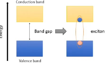
The physical important parameter of semiconducting materials is the width of the energy gap, which is the minimum energy required to promote an electron from the ground state valence energy band to the conduction energy band (see Fig.1), forming an exciton.2 The
energy gap is a fixed parameter in solids of macroscopic size and depends on the material’s nature. The situation is different in nano-semiconductors with sizes smaller than ~ 10 nm, because of their dimensionality and quantization. This gap is related to the quantum system for which electronic excited states feel the presence of the particle border. The electronic levels respond to any change in the particle size by adjusting their energy. This feature is known as quantum confinement, and the nanomaterials with this characteristic are referred to as quantum dots (QDs).3,4
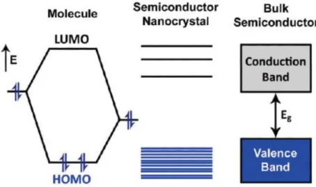
9 Colloidal quantum dots can be considered as an intermediate class of material between atoms and bulk. The comparison between the energy levels of nanocrystals and bulk semiconductors on the one side and molecular structures on the other side is exemplified by the figure 2.
Figure 2. Evolution of electronic levels from molecule to bulk material
Nanocrystals are classified according to the categories given by Pokropivny and Skorokhod (2007)5 in:
• (3D) Three-dimensional structures (nanocups).
• Two-dimensional (2D) structures such as nanofilms, nanosheets, nanoplatelets (NPLs), etc.
• One-dimensional (1D) materials as nanowires (NWs), nanorods (NRs), • Zero-dimensional (0D) structures as nanospheres, nanodots, etc.
In bulk semiconductors, the exciton can move freely in all directions. When the size of the nanocrystals semiconductors is smaller than the radius of Bohr of the exciton, the charge carriers (electron and hole) become spatially confined; this effect is known as quantum confinement regime. Therefore, the exciton’s size outlines the transition between the bulk crystal properties and the quantum confinement. The quantum confinement displays size-dependent absorption and fluorescence spectra. In addition, depending of the degree of confinement and the dimensionality, the band gap can be tuned to a define energy.
10
I. 2 Optical properties of CdSe semiconductor
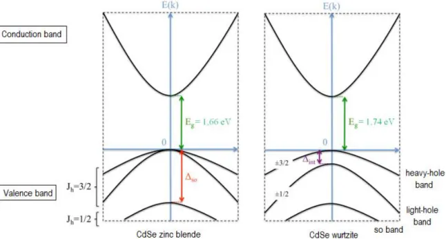
CdSe nanoparticles are II-VI semiconductors with interesting optical properties determined by their size and structure. The conduction band is typically composed of the s orbitals of cadmium, which is degenerate twice by the electron spin. The conduction band commonly consists of the orbitals px, py, and pz of selenium and is degenerated 6 times by the
hole spin and the orbital moment. The valence band also comprises three bands, heavy holes (hh), light holes (lh) and the split off bands (so). The II-VI semiconductors usually present an interaction between the spin s and the orbital moment l of a particle resulting in a quantum number (J = s + l). In the valence band, the quantum number J takes different values in the hole bands (Jh = 3/2 and Jh = 1/2) and they are separated by an energy ∆so. In the case of the
würzite structure, the hh and the lh are separated by an energy ∆int (Fig. 3).6
Figure 3. Schematic representation of the energy band structure of zinc blende and würzite CdSe nanocrystals.
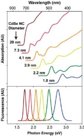
The spacing between the bands diminishes when atoms are added to the particle. When the semiconducting nanocrystals are of the same composition but of different sizes their optical properties change. Upon excitation at energy bigger than the band gap an electron-hole pair (exciton) is created between the valence and the conduction band. This is noticeable on the UV-visible absorbance spectra (Fig. 4). For incident energies below the band gap the material does not absorb light. For an incident energy corresponding to this gap,
Flores Arias Yesica – doctoral Thesis - 2018
11 one can observe a transition known as the excitonic transition. And for even higher energies, the absorbance continuously increases since all transitions in the conduction band can occur. The exciton then relaxes in a radiative manner leading to a photoluminescence (PL) spectrum made of a single narrow peak corresponding to the splitting between the band edges. As consequences, since the bigger the nanocrystals are the smaller the gap is, the emission color of the band-edge PL shifts continuously, towards lower energies, as the size of the nanocrystals increases, and so does the excitonic transition in absorbance (Fig. 4). The distance between the electron and hole in a semiconductor is known as the Bohr radius of the exciton (aB). The minimum value for the band gaps corresponds to the bulk material, value
that can be reached when the radius of the crystals is of the order of the Bohr radius of the exciton.1
Figure 4. UV- visible spectra of various size QDs (top). Size-tunable fluorescence of quantum dots (bottom).
12
I. 3 Synthesis
Over the past several years considerable effort has been placed on the controlled synthesis of semiconducting nanocrystallites. Achieving an appropriate high quality synthetic method is crucial to interpreting optical properties, and such an interpretation can be challenging because of different phenomena associated to polydispersities in size and shape and poor crystallinity.7 QDs have been prepared by physical and chemical methods:
I. 3. 1 Physical methods
Thermal evaporation (TED) is a physical vapor deposition (PVD) technique usually applied to fabricate an extensive range of thin films. This technique is performed in vacuum and the solid precursor is heated at high temperature (above its melting point) until its evaporation. The stream of vapors moves towards a substrate and condenses in the form of thin films. This method allows a better control of different parameters such as thickness, composition, grain size, morphology. For instance, CdS and ZnS of one-dimensional nanoshape such as nanowires and nanoribbons were fabricated on silicon substrates in the presence of Au catalyst by thermal evaporation. The temperature and the concentration of the subtrates were the critical experimental parameter for the formation of different morphologies.8,9
Electron beam evaporation is assigned as electron beam physical vapor deposition. In this method, an energetic beam of electrons strikes the material source in a vacuum container and the atoms at the surface collect enough energy to evaporate. The evaporated atoms condense in the form of a coating on the substrate. Electron beam evaporation produces attractive control deposition and morphology with low contamination.5
These vacuum techniques have not been studied during this Ph.D. since we intended to develop a soft method to synthesize colloidal hybrid nanocrystals.
I. 3. 2 Chemical methods
The physical methods described above present two main disadvantages: i) they require ultra-high vacuum technologies that are expensive and heavy to process and ii) QDs are produced in small quantities. Therefore chemists have sought to produce inexpensive and bench experiments able to easily produce batches of colloidal nanocrystals. Here we will
13 shortly present an overview of different synthetic techniques to produce colloidal nanocrystals.
The solvothermal process5 involves the chemical reaction of precursors using organic solvents, performed at a temperature that is higher than the boiling point of the solvent. In this method, physicochemical reactions take place at high pressure and temperature. This is so because the growth process is carried out in a container known as autoclave (made of Teflon/stainless steel). Precursors and solvents react at a specific temperature for different durations. The process introduces organic solvents such as long alkylamines (octadecylamine) and more recently short-chain alkylamines (ethylenediamine). The structure, morphology, size, crystal shape and properties of the semiconductor nanocrystallites are strongly influenced by different parameters such as solvent, temperature conditions, precursors, concentration and processing time. The solvothermal technique uses a simple and nontoxic solution route, without tedious size-selection processes and expensive organometallic/non metallic precursors. The advantages of this environment-friendly solvothermal technique include the production of size controlled monodisperse nanocrystals like nanospheres, nanowires, nanorods and nanotripods.5,10 For instance, nanorods of CdE (E=S, Se, Te) have been successfully synthesized with a solvothermal method.11
The Sol-gel method5 is a chemical synthesis route used to make materials via polycondensation of molecular species from a solution. This method usually consists of dispersed colloidal particles in a solvent (a sol), which is chemically converted into a gel (aggregated sol particles) followed by condensation in the form of solid nanostructures. Sol-gel is a wet chemical method that embraces 2 steps: the first comprises hydrolysis and polycondensation reactions of the precursors to prepare the gels, and the second is sintering of amorphous colloidal into compact powder. This process facilitates the production of nanospheres and nanorods.
Pyrolysis (or hot injection) is one of the most used techniques for the production of high quality nearly monodisperse samples of CdS (E= S, Se, Te) nanometer size crystallites. The synthesis begins with the rapid injection of metal-organic precursors into a hot coordinating solvent (120-360°C) to produce temporally discrete homogenous nucleation. CdSe QDs can be prepared from a variety of cadmium precursors, as alkyl cadmium compounds and some cadmium salts (cadmium oxide, cadmium acetate and cadmium carbonate) combined with a selenium precursor at room temperature (r.t), which is prepared
14 by dissolving Se powder in trioctylphosphine (TOP) and making a TOP-Se complex. The reagent mixture is rapidly injected to the hot surfactant solvent TOPO (180-210°C°) that results in a short burst of homogeneous nucleation, which is quickly quenched by the fast cooling of the introduction of room temperature reagents.37 One of the main disadvantages of the pyrolysis process was that it required special experimental precautions because of the extreme high reactivity of the cadmium precursors that also used to restrain the size of the batches.1 Nevertheless, this problem has been solved over the past decade by using cadmium oxide as stable precursor.
The template method is an easy technique commonly used to prepare nanomaterials.12 Compared to traditional techniques, the template route allows the efficient control of particles’ size, structure and morphology. This technique includes three steps. The first is the preparation of the template. Second, another synthetic approach as sol-gel and hydrothermal method is employed to prepare the main material based on the function of template. Third, the template is removed. The template method is usually divided in 2 groups depending on the use of a hard template or a soft template.
The hard template is a rigid material that controls the dimensions and the morphology of the material.12 For the preparation of nanomaterials, using porous materials, the precursor is likely to crystallize outside or inside of the pores of the template. The dimension of the pores will contain the unit cell of the material and will form a crystal material, having the same structure as the pore. The material obtained by this process presents good dispersity and homogenous size. However, the removing of the templates usually causes the collapse of part of the pores structure, which affects the final product.
The soft template method requires simple equipment and usually allows good reproducibility.12 It begins with the formation of an aggregate of organic molecules (surfactants, polymers) by intermolecular interactions. And these aggregates are used as templates. On the surface of or inside these templates some inorganic species are deposited by different methods to form particles with different sizes and shapes. Surfactants and polymers are often used as templates. One of the disadvantages of the method is the stability of the aggregates: ordered structures are formed only if the template has a strong interaction with the precursor.
15
I. 4 Shape control
The study of the formation and shape evolution of colloidal semiconducting nanocrystals are of great importance to understand the nucleation and growth process. The nucleation is the first step in the growth of any nanocrystal. Through a fluctuation of the medium in which the nanocrystals are formed, several atoms assemble to a small crystal seed that is thermodynamically stable, and thus does not fall into free atoms or ions.1 Then, growth can be controlled by the kinetics of the reaction or the use of surfactants.
I. 4. 1 Kinetic control
The control of the growth kinetics of II-VI semiconductors can modify the shape of the particles from a spherical to rod morphology. This also implies that kinetic control can be used to manipulate the average particle size and size distribution. The model of LaMer and Dinegar3 exemplifies the correlation between the solute concentration and different reaction periods. The model includes three periods that start by a supersaturation (I), then a nucleation event (II) followed by a rapid growth (III) and finally by a slower growth by Ostwald ripening (IV) (Fig. 5). Peng et al. further studied the growth of CdSe nanocrystals and observed the shape evolution from dots to rods. They showed that the growth process also develops in two steps, related to the concentration of the monomers: focusing and defocusing.13
The authors reported that chemical potential of elongated nanocrystals is commonly high compared to dot-shaped nanocrystals. This means that the growth of elongated nanocrystals will take place when the chemical potential of the monomers in solution is relatively high, and usually this occurs when the activity of the monomers (monomers concentration) is also high. This means that by simply increasing the monomers concentration in the solution, dot-shaped CdSe nanocrystal were transformed in rod-shaped. When the Cd concentration of the monomer is higher than the solubilities of all the particles, the nanocrystals grow only along a unique axis. And also some variables as ratio and volume of the crystal increase faster which results in a one-dimensional growth stage (1D-growth stage) and the size distribution narrows down. This is the focusing of size distribution, which leads to a close formation of monodisperse colloidal nanocrystals.
16
Figure 5. La Mer's model describing the nucleation and growth process for monodisperse colloidal particles.
But if the Cd monomer concentration is at an intermediate level the crystal grows simultaneously in three dimensions. The ratio stays constant and the crystal volume increases. In addition to the concentration of the monomers, thermodynamic parameters (in addition to temperature) also promote the three-dimensional growth. Indeed, when the monomer concentration drops below the critical point, the length of the rods diminished and their width increased and the size distribution broadens. This means that the anisotropic structure is not thermodynamically favourable as the monomers move away from the rod and grow onto the sides promoting one-dimension to two-dimension intraparticle ripening (1D to 2D ripening). In this process with sufficient time, the quantum rods can progress into dot-shaped. This is the defocusing of size distribution (Ostwald ripening).14,15
I. 4. 2 Shape control by the surfactants
The performance of surfactants (or surface ligands) has initially been optimized to promote colloidal stability rather than shape and size control. However, surfactants, more than making the nanocrystals dispersible in organic solvents also show extraordinary control over crystal growth at the nanoscale and produce well-defined morphologies.
On the basis of the above facts, to preserve the control of the growth rates, different surfactants need to be used. Peng’s group15,16 further discovered that pure TOPO is not
convenient to obtain quantum rods. The presence of pure TOPO induces a faster growth at the high monomer concentration that causes big rod-like particles. The additional components in technical grade TOPO generate slow growth kinetics. To simulate the presence of impurities in technical TOPO (alkyl phosphonic and phosphinic acids - that bind relatively strongly to
17 cadmium), they add a hexyl-phosphonic acids (HPA) that coordinates stronger than TOPO to cadmium. That allows adjusting the growth rate and improves the shape control of the nanocrystals.
Highly hydrophobic surfactants (e.g double tail surfactants) have been demonstrated to be exceptional shape directing agents over crystal growth at nanoscale due to a better surface passivation ability. Double tail surfactants are more hydrophobic and surface active in comparison to the single tail surfactants. When a surfactant is highly hydrophobic as in the case of didodecyl dimethylammonium bromide (DTAB) the formation of cubes with {100} crystal planes is generated. However weaker hydrophobicity (as dimethylene bis- (dodecyldimethylammoniun bromide) preserves hexagons bound with {111} crystal planes.17
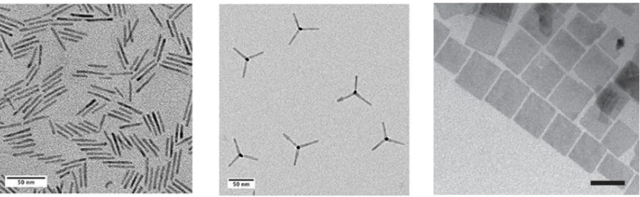
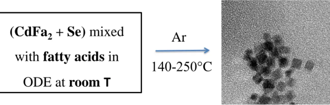
The parameters cited above allowed different authors to synthesize CdSe QDs,18 Q-rods,19 tetrapods,20 nanoplatelets21 and quantum rings (Fig. 6).22 Among CdSe nanocrystals,
we will focus now on nanoplatelets.
Figure 6. TEM micrographs of different CdSe nanocrystals: from left to right, rods, tetrapods and nanoplatelets.
I. 5 CdSe Nanoplatelets: synthetic aspects
Two-dimensional CdSe semiconductor nanoplatelets or quantum disks have been obtained in two different crystal structures würtzite and zinc blende. The latter has been synthesized by Ithurria and Dubertret in 200821 and is one of the most of interesting kind of
nanocrystals thanks to their unique optical properties.
An approach to the synthesis of zinc blende nanoplatelets is in some way the soft template method previously mentioned. The synthesis for the CdSe NPLs relies on fatty acid
18 ligands that bond on the basal planes of the nanoplatelets or quantum disk. To explain, the formation CdSe nanoplatelets, the groups of Peng on the one side and Dubertret, on the other side do not agree on the mechanism of formation of the NPLs and therefore on the best conditions to get them. Dubertret’s group, the initiator of nanoplatelets, established that using cadmium acetate (CdOAc2) or short carboxylates as precursor is necessary to trigger the
lateral extension of the NPLs. On the contrary, Li and Peng23 claimed that any fatty acid can be used to get NPLs such as cadmium butanoate (CdBu2), and cadmium octanoate (CdOc2).
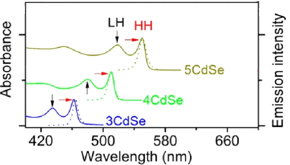
Nevertheless, both groups concluded that fatty acids are anyway necessary in the synthesis of 2D CdSe nanostructures, either by using these fatty acids as precursors or by adding it during the reaction. In fact, the temperature range of the synthesis is determined by the hydrocarbon chain length of the fatty acids which must be between 140 and 250°C in order to get platelets (Fig.7).
Figure 7. Reaction strategy for obtaining CdSe nanoplatelets. CdFa2 represents the
cadmium fatty acid salts.
Among fatty acids that can be used for the synthesis of NPLs, Peng and co-workers tried two fatty acids, stearic acid and decanoic acid (Fig. 8). The results revealed that the up temperature limit increased as the chain length of the fatty acids raised. Therefore, the temperature of apparition of quantum dots occurred early for the dodecanoic acid. The figure 8 show the maximum absorbance of the CdSe nanoplatelets obtained at 180°C for the dodecanoic acid and 240°C for the stearic acid. Li and Peng attributed this effect to the influence of the hydrocarbon chain on the thermal stability of the NPLs, one of the key parameters on the soft-template growth mechanism.
(CdFa
2+ Se) mixed
with fatty acids in
ODE at room
T
Ar
140-250°C
19
Figure 8. UV-vis of CdSe quantum disks grown at different temperatures and obtained with stearic acid (left) and decanoic acid (rigth). The inset shows the absorbance of the excitonic
absorption versus the temperature of the reaction.
It should be pointed out that the lateral dimensions rely upon the concentration of fatty acids, the chain length of fatty acids, and the reaction temperature and the lateral size can be tuned from some nanometers to a few hundred nanometers. It was found that the lower the concentration of the fatty acids the larger the lateral dimension was obtaining. But also increasing the length of fatty acids can lead to the same result. Regarding the effect of the temperature, low temperature resulted in quantum disk of small lateral dimensions.23 The continuous injection of precursors also induces the growth of lateral extension in different nanoparticles such as CdTe and CdSe NPLs. Another variable to control on these NCs is the thickness.
Further studies21 demonstrated that the latter the acetates are added to the synthesis the
thicker the NPLs would be formed. In the case of CdS, it was shown that low temperature and shorter alipathic chains induce thinner nanoplatelets. The NPLs formation appears between 130 and 140°C in a period of few minutes, the low temperature limit is possibly determined by the activation of elemental Se in the reaction system. The growth of these ultrathin nanocrystals is achieved at higher temperature ranging from 130°C to 250°C whereas at lower temperature the formation of würzite NPLs take place.24 Higher temperature could eliminate the packing of ligands that is critical for the formation of soft-template process.
20 Li and Peng also studied the monomers concentration effect on the formation of nanoplatelets. We mentioned in paragraph I.4.1 that in order to get II-IV quantum rods, the concentration of the monomers should be sufficiently high to induce the 1D- growth. However, they didn’t found a relevant difference by varying the precursor concentration. One possible explanation is that the Se powder used for the synthesis was no activated, owed to the low temperature reaction used for analyzing.
They also observed that the Cd and Se precursors ratio should be necessary higher than 1:1 for the growth of CdSe disks. This result is consistent with to the fact that in two- dimensional nanocrystals both the top and the bottom are Cd atoms terminated.23
Dubertret’s group24 demonstrated that CdSe nanoplatelets growth begins with the
nucleation of ̴ 2 nm diameter nanocrystals seeds. These small nanocrystals would then immediately associate, to form NPLs that gradually expand their lateral dimension (Fig. 9). The formation of nanoplatelets could start by the self-assembly of this well-defined seed to extend laterally (path 1). The self-organization of small cluster that assemble in patches has been observed in ultrathin PbS nanoplatelets with a rock salt crystal structure (path 3). These seeds have two cation-rich facets that are bound to ligands and also can extend laterally thanks to in situ continuous reaction of Cd and Se precursors on the NPLs edges (path 2).
21
Figure 9. Evolution of the CdSe NPLs lateral extension. It begins with the formation of small seeds. The seeds self-organize to assemble and form the lateral extension (path 1).
Lateral dimensions extend by continuous reaction of precursors (path 2).
I. 6 Optical properties of CdSe nanoplatelets
In recent years, colloidal quasi-two dimensional (2D) II-VI semiconductor nanocrystals (NPLs) such as CdS, CdTe and CdSe has gained growing interest due their original optical properties that empower advanced optoelectronic devices. These flat nanocrystals have electronic lateral dimensions that are much larger than the exciton Bohr radius. But their thickness is similar to those of the ultrathin semiconducting quantum wells (QWs).25
Cadmium-based nanoparticles offer26 advantageous features such as a strong oscillator strength and direct bandgaps in the visible region. Thanks to these, many properties of these NPLs such as size, shape, composition, crystal structure or surface ligands can be analyzed by using spectroscopic studies as fluorescence, absorption, photoluminescence excitation and fluorescence lifetime.
22 Contrary to the würtzite structure the zinc blende NPLs present their thickness along the short axis direction (001). The others two long axis directions correspond to their lateral NPLs planes. The thickness control is quantized to an integer number of monolayers (MLs). Recently, it has been synthesized 3 different populations of nanoplatelets with thickness of 0.9, 1.2 and 1.5 nn. This thickness is characterized by monolayers of CdSe with corresponding numbers of Se layers, which we term 3ML, 4ML, 5ML; maxima of exciton absorption can be found at 463, 513, and 550 nm with lateral dimensions of 60±5 nm by 40±7 nm for 3ML, 27±3 nm by 7±2 nm for 4 ML, 25±3 nm by 10±1 nm for 5ML.27,28
The emission quantum yield (QY) has been reported around 50% for the 5ML, between 55 and 34 % for 4ML an 10% for 3ML. The PL lifetime is much faster in NPLs than in 0D QDs, it can go from few nanoseconds at room temperature to 300 ps at 4 K, which makes the NPls the fastest colloidal emitters until now.29
For each population of NPLs we can identify on the absorbance spectrum two transitions: a sharp peak that corresponds to the first excitonic transition electron/heavy hole (lowest energy), and a broader signal corresponding to the electron/light hole transition (highest energy). These two transitions are at 513 nm and 480 nm for the 4 ML (Fig. 10).25
Figure 10. Absorption (solid lines) and photoluminescence spectra (dotted lines) emitting at 462nm (3ML), 512nm (4ML), 550 nm (5ML) CdSe nanoplatelets.
23
I. 6. 1 Effect of the NPLs thickness and lateral dimensions
The strong quantum confinement in the NPLs is only in the vertical direction, meaning that the only parameter that defines the exciton energy is the thickness of the nanoplatelets.25 The strong quantum confinement, at the same time, is reflected in a extremely narrow intense bands on both absorption and PL spectra with full width at half maximum (fwhm) close to kT tipically between 7 and 10 nm at room temperature and a small Stokes shift.30,31
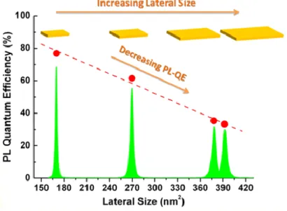
On the other hand, it was reported that increasing the lateral size of NPLS does not produce any spectral shift on PL. However, growing the lateral dimensions has been shown to decrease the Photoluminescence efficiency (PL-QE) and to greatly accelerate the photoluminescence decay rate (Fig. 11). To explain this observation it was found that a broad part of the population of NPLs present hole traps and the probability to find these defects such as Cd vacancy in the CdSe NPLs increases as the lateral area increases. Therefore, this suggests that in ensemble NPLs where the mean lateral size is larger the nonradiative trap channel is introduced by the defected NPls subpopulation.25
Figure 11. Evolution of the photoluminescence quantum efficiency with increasing lateral size.
Dubretret and co-workers concluded that the zinc blende NPLs presents an atomically flat surface.26 And being atomically flat enhances the interaction between ligands decorating their surface compared with highly curved surfaces.31
24
I. 6. 2 Effect of the ligand
Ligands play an important role in the colloidal nanocrystal semiconductors properties. For exemple, ligands molecules can be employed as precursors in the synthesis of NCs; they can influence the nucleation and growth kinetic as well as the morphology, size control and crystalline structure of the NCs as we have studied before. They also contribute to the colloidal, chemical and photo-stability in several media by modifying the functionality and reactivity of the NCs. Moreover, it determines significantly the physical properties of the NCs. Among these features, studying the interactions between the ligand and the interphase in the 2D semiconductors nanoplatelets is becoming of great interest.
A key advantage of the NPLs compared to the QDs and nanorods is the surface chemistry, while for QDs and nanorods their highly curved surface introduce disorder in the ligand layer, NPLs present a relatively large and atomically flat surface.
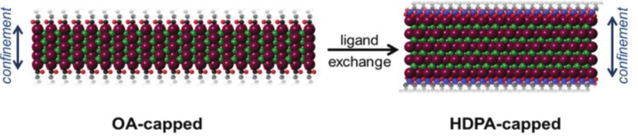
Recently the group of Antanovich32, evidenced the impact of surface passivating ligands on the optical and structural properties of zinc blende CdSe nanoplatelets. They observed that upon ligand-exchange of native oleic acid (OA) with hexadecanethiol (HDT) and n-hexadecylphosphonic acid (HDPA) on the surface with different monolayers CdSe nanoplatelets the optical spectra become significantly red-shifted (Fig. 12).
25
Figure 12. Absorbance (black) and emission spectra (red) of 4ML CdSe NPLs coated with oleic acid (OA), hexadecanethiol (HDT), hexadecylphosphonic acid (HDPA).
Dashed lines show the first absorption maxima.
It has been reported for QDs that some capping ligands as phenylchalcogenols Ph-X (X= SH, SeH, TeH) and non-innocent ligands (e.g. phenyldithiocarbamate) can induce large red-shift in PL around 10 -40 nm. Nevertheless, HDPA and HDT are ligands that modify the confinement and exciton transition energy by altering the NCs band gap. They demonstrated that the exciton energy shift was related to structural changes. They exhibited by XRD that the functionalization of the NPLs with organic ligands induces an anisotropic distortion of the unit cell by ligands comprising a contraction of the lateral direction and an expansion in the thickness direction of the ZB unit cell (Fig. 13). This means that cubic symmetry of the ZB
26 CdSe lattice is diminished into a tetragonal symmetry. Since the lattice distortion can be attributed to several elements, the observed lattice strain magnitude was attributed to the head group interaction with the surface Cd atoms of the NPLs. This assumption is in line with several reports that indicate that an increase of ligand coverage could generate the augmentation of repulsive interaction of headgroups, leading to tensile strain. Therefore, ligand induced strain alters the well thickness and hence the exciton confinement.32
Figure 13. Proposed scheme of anisotropic lattice distortion by ligand exchange.
I. 7 Self-assembly of CdSe nanoplatelets
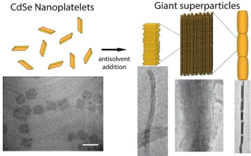
In 2013, Dubertret and coworkers33 reported the self-organization of CdSe nanoplatelets into stacks to form 1D-superlattice through the addition of an antisolvent in the colloidal nanoplatelets solution. They noted that addition of ethanol could trigger the formation of anisotropic supracrystals. Hassinen and coworkers34 exposed that short-chain alcohols remove and replace the carboxylate ligands at the surface of QDs nanocrystals. Therefore, the addition of ethanol could restrain the steric repulsion imposed by the oleic acid brush making possible the nanoparticles stacking. Another explanation comes from the fact that ethanol is a bad solvent for the aliphatic chain of the carboxylate ligands. In other terms, the contact between aliphatic chains of the oleic acids is energetically favoured when the amount of ethanol is increased. In these supraparticles, the NPL building blocks are oriented with their lateral planes that are perpendicular to the long axis of the column-like assemblies, whose length can contain about 106 individual nanoparticles (Fig. 14).
27
Figure 14. Self-organization of ZB CdSe nanocrystals into 1D superparticles
Interestingly, the light emitted by these microneedles is steadily polarized in the direction perpendicular of the principal direction of the microneedles. This indicate the polarization in the plane of an individual nanoplatelet (Fig 15).33
Figure 15. Epifluorescence measurements of stacked NPLs versus the polarization direction.
Another approach to promoting the self-organization of CdSe NPLs is by the slow evaporation of colloidal solution. Abécassis and coworkers used oleic acid followed by a slow drying and then a redispersion to induce the self-assembly into micrometre-long threads. They detected by fluorescence microscopy that these threads can periodically break and restore dynamically. Moreover, free NPL join to both terminations of the existing threads with no formation of new chains. In other terms, the length of threads increases through the addition
28 of NPLs (Fig. 16). For this reason the 1-dimensional superstructures was named living polymers. Two different forces may favour the self-assembly of the system: Van der Waals and depletion interactions. The first one destabilize colloidal solution within time and the second depends linearly on the oleic acid concentration.35
Figure 16. Dependence of the threads average length on the number of NPL added.
The gradual process of formation of stack of nanoplatelets was studied by Guzelturc et
al.36 They observed that the photoluminescence intensity decreases as the NPLs are formed
29
Figure 17. Influence of the stacking of NPLs on the fluorescence properties upon the addition of ethanol.
They showed that the quenching of the photoluminescence was linked to the existence of exciton migration. According to their explanation, the excitons migrate from one platelet to another within the stacked NPLs assemblies until they come to a non emissive well (Fig. 18). It has been reported that CdSe NCs bearing poorly passivated surfaces sites, crystal and surface defects can outcome in non-emmisive nanocrystals. For instance, hole trapping was associated to Cd vacancies and poor surface passivation in CdSe NCs leading to a non-radiative recombination of the exciton. Non-non-radiative recombination is when an electron in the conduction band recombines with a hole in the valence band and the excess of energy is emitted in the form of heat.37 As a consequence, the existence of non-emissive platelets in stacked quantum wells can strongly decrease the photoluminescence intensity.36
30
Figure 18. Scheme of nonemissive NPL within the stacks leading to hole trapping on the exciton migration, causing non radiative recombination which results in the
photoluminescence emission decrease of the stacked NPLs.
In order to understand the influence of the nanocrystal environments, the spectroscopy of a single nanoplatele was analyzed at room temperature and at 20 K. Tessier et al. 38 compared the emission spectra of single CdSe NPLs on a glass surface in air with the emission of CdSe NPLs in solution. Surprisingly the emission spectrum of the single ones was very similar to the ones of unstacked ensembles (Fig. 19). This similarity is because there is no inhomogenous broadening in these ultrathin NPLs which is common detected for spherical and rodlike particles) and that is caused by size alteration. They also observed that the fwhm of single NPL is slightly bigger than the unstaked ensemble measurement. This behavior may be related to the fact that the single NPL were exposed in air which results in various emitting states. And these different emitting states may correspond to the rearrangements of the ligands as a consequence of the reversible interaction of the basal planes of the NPLs with H2O and/or O2 and photo-oxidation during illumination in air.38
31
Figure 19. Emission spectra of NPLs in solution and on single platelet on a glass substrate at room temperature.
At 20 K, the fwhm of the PL spectrum of a single NPL decreases at low excitation, while the fwhm of the unstacked NPLs becomes larger (Fig. 20). The large inhomogenous broadening detected in unstacked nanoplatelets was related to spectral diffusion. Meaning that local variations of the enviroments can outcome in different emission maxima for every NPL.
Figure 20. a) Emission spectra of a single NPLs (553 nm) and b) of an ensemble NPLs (553 nm) at 20 K.
Later the same authors39 demonstrated that stacked NPLs show a different photoluminescence spectrum compared to the non-stacked ensembles at cryogenic temperatures. They exhibited the apparition of a second low energy line in the NPL self- assembly at 20 K (Fig. 21).
32
Figure 21. Emission spectra of dispersed NPLs (553 nm) (left) and stacked nanoplatelets at 20 K.
This red shifted emission line that begins to show up at 120 K was attributed to the phonon line-emission replica. According to their interpretation, a photon emitted in the main line (band edge transition) can be reabsorbed by neighbouring NPLs because the Stokes between the main line emission and the first absorption exciton is too small.
However, when the NPL emit the photon in the phonon line emission, the photon cannot be reabsorbed by stacked NPLs. The model proposed predicts the increase of the intensity of the phonon as the lateral dimensions of the NPLs increase, which explains why the phonon line emission is not observed when the NPLs are well dispersed or in single NPLs. In addition, the difference between the first and the second emission line is independent of the NPLs size, thickness, and surface ligand interaction. Interestingly, this energy gap is related to the character of the material (25 meV for CdSe and 20 meV for CdTe) (Fig. 22).39
Figure 22. Emission spectra of an ensemble stacked NPLs (553 nm) demostrating the energy gap between the high energy line and the low energy line.
33 The NPLs optical properties are very much influenced by the environment (ligands, stacking, solvent, among other factors). It is both an advantage and a difficulty. Therefore we need to put attention to many parameters when preparing hybrids nanocrystals. At the same time optical spectroscopies can efficiently probe the correlations between the structure and the properties of such hybrid nanocrystals.
34
I. 8 References
1 A. L. Rogach, Semiconductor nanocrystal quantum dots, Wien-New York Springer.
2 A. M. Smith and S. Nie, Semiconductor Nanocrystals: Structure, Properties, and Band Gap Engineering, Accounts Chem. Res., 2010, 43, 190–200.
3 V. I. Klimov, Semiconductor and Metal Nanocrystals: Synthesis and Electronic and
Optical Properties, CRC Press, 2003.
4 L. Cornejo, El porqué las diferentes propiedades de las nano partículas, http://nuevastecnologiasymateriales.com/el-porque-las-diferentes-propiedades-de-las-nano-particulas/, (accessed 2 April 2018).
5 A. Majid and M. Bibi, Cadmium based II-VI Semiconducting Nanomaterials, Springer International Publishing, Cham. 2018.
6 E. Cassette, PhD Thesis, Université Pierre et Marie Curie-Paris VI, 2012.
7 C. B. Murray, D. J. Norris and M. G. Bawendi, Synthesis and characterization of nearly monodisperse CdE (E = sulfur, selenium, tellurium) semiconductor nanocrystallites, J. Am.
Chem. Soc., 1993, 115, 8706–8715.
8 S. Kar and S. Chaudhuri, Shape Selective Growth of CdS One-Dimensional Nanostructures by a Thermal Evaporation Process, J. Phys. Chem. B, 2006, 110, 4542– 4547.
9 Formation of ZnS nanostructures by a simple way of thermal evaporation, J. Cryst.
Growth, 2003, 258, 225–231.
10 J. Xu, J.-P. Ge and Y.-D. Li, Solvothermal Synthesis of Monodisperse PbSe Nanocrystals,
J. Phys. Chem. B, 2006, 110, 2497–2501.
11 Y. Li, H. Liao, Y. Ding, Y. Fan, Y. Zhang and Y. Qian, Solvothermal Elemental Direct Reaction to CdE (E = S, Se, Te) Semiconductor Nanorod, Inorg. Chem., 1999, 38, 1382– 1387.
12 Y. Xie, D. Kocaefe, C. Chen and Y. Kocaefe, Review of Research on Template Methods in Preparation of Nanomaterials, J. Nanomater., 2016, 2016, 1–10.
13 M. Meyns, Metal-semiconductor hybrid nanoparticles: Halogen induced shape control,
hybrid synthesis and electrical transport, Anchor Academic, 2014.
14 X. Peng and J. Thessing, in Semiconductor Nanocrystals and Silicate Nanoparticles, Springer, Berlin, Heidelberg, pp. 79–119.
35 15 Z. A. Peng and X. Peng, Nearly Monodisperse and Shape-Controlled CdSe Nanocrystals via Alternative Routes: Nucleation and Growth, J. Am. Chem. Soc., 2002, 124, 3343– 3353.
16 Z. A. Peng and X. Peng, Mechanisms of the Shape Evolution of CdSe Nanocrystals, J. Am.
Chem. Soc., 2001, 123, 1389–1395.
17 M. S. Bakshi, How Surfactants Control Crystal Growth of Nanomaterials, Cryst. Growth
Des., 2016, 16, 1104–1133.
18 X. Peng, L. Manna, W. Yang, J. Wickham, E. Scher, A. Kadavanich and A. P. Alivisatos, Shape control of CdSe nanocrystals, Nature, 2000, 404, 59–61.
19 A. Wolcott, R. C. Fitzmorris, O. Muzaffery and J. Z. Zhang, CdSe Quantum Rod Formation Aided By In Situ TOPO Oxidation, Chem. Mater., 2010, 22, 2814–2821.
20 Q. Pang, L. Zhao, Y. Cai, D. P. Nguyen, N. Regnault, N. Wang, S. Yang, W. Ge, R. Ferreira, G. Bastard and J. Wang, CdSe Nano-tetrapods: Controllable Synthesis, Structure Analysis, and Electronic and Optical Properties, Chem. Mater., 2005, 17, 5263–5267. 21 S. Ithurria and B. Dubertret, Quasi 2D Colloidal CdSe Platelets with Thicknesses
Controlled at the Atomic Level, J. Am. Chem. Soc., 2008, 130, 16504–16505.
22 I. Fedin and D. V. Talapin, Colloidal CdSe Quantum Rings, J. Am. Chem. Soc., 2016, 138, 9771–9774.
23 Z. Li and X. Peng, Size/Shape-Controlled Synthesis of Colloidal CdSe Quantum Disks: Ligand and Temperature Effects, J. Am. Chem. Soc., 2011, 133, 6578–6586.
24 S. Ithurria, G. Bousquet and B. Dubertret, Continuous Transition from 3D to 1D Confinement Observed during the Formation of CdSe Nanoplatelets, J. Am. Chem. Soc., 2011, 133, 3070–3077.
25 M. Olutas, B. Guzelturk, Y. Kelestemur, A. Yeltik, S. Delikanli and H. V. Demir, Lateral Size-Dependent Spontaneous and Stimulated Emission Properties in Colloidal CdSe Nanoplatelets, ACS Nano, 2015, 9, 5041–5050.
26 C. Bouet, M. D. Tessier, S. Ithurria, B. Mahler, B. Nadal and B. Dubertret, Flat Colloidal Semiconductor Nanoplatelets, Chem. Mater., 2013, 25, 1262–1271.
27 C. She, I. Fedin, D. S. Dolzhnikov, P. D. Dahlberg, G. S. Engel, R. D. Schaller and D. V. Talapin, Red, Yellow, Green, and Blue Amplified Spontaneous Emission and Lasing Using Colloidal CdSe Nanoplatelets, ACS Nano, 2015, 9, 9475–9485.
28 S. Jana, T. N. T. Phan, C. Bouet, M. D. Tessier, P. Davidson, B. Dubertret and B. Abécassis, Stacking and Colloidal Stability of CdSe Nanoplatelets, Langmuir, 2015, 31, 10532–10539.
36 29 E. Lhuillier, S. Pedetti, S. Ithurria, B. Nadal, H. Heuclin and B. Dubertret,
Two-Dimensional Colloidal Metal Chalcogenides Semiconductors: Synthesis, Spectroscopy, and Applications, Accounts Chem. Res., 2015, 48, 22–30.
30 A. W. Achtstein, A. Antanovich, A. Prudnikau, R. Scott, U. Woggon and M. Artemyev, Linear Absorption in CdSe Nanoplates: Thickness and Lateral Size Dependency of the Intrinsic Absorption, J. Phys. Chem. C, 2015, 119, 20156–20161.
31 E. Lhuillier, S. Pedetti, S. Ithurria, B. Nadal, H. Heuclin and B. Dubertret, Two-Dimensional Colloidal Metal Chalcogenides Semiconductors: Synthesis, Spectroscopy, and Applications, Accounts Chem. Res., 2015, 48, 22–30.
32 A. Antanovich, A. W. Achtstein, A. Matsukovich, A. Prudnikau, P. Bhaskar, V. Gurin, M. Molinari and M. Artemyev, A strain-induced exciton transition energy shift in CdSe nanoplatelets: the impact of an organic ligand shell, Nanoscale, 2017, 9, 18042–18053. 33 B. Abécassis, M. D. Tessier, P. Davidson and B. Dubertret, Self-Assembly of CdSe
Nanoplatelets into Giant Micrometer-Scale Needles Emitting Polarized Light, Nano Lett., 2014, 14, 710–715.
34 A. Hassinen, I. Moreels, K. De Nolf, P. F. Smet, J. C. Martins and Z. Hens, Short-Chain Alcohols Strip X-Type Ligands and Quench the Luminescence of PbSe and CdSe Quantum Dots, Acetonitrile Does Not, J. Am. Chem. Soc., 2012, 134, 20705–20712.
35 S. Jana, P. Davidson and B. Abécassis, CdSe Nanoplatelets: Living Polymers, Angew.
Chem. Int. Ed., 2016, 55, 9371–9374.
36 B. Guzelturk, O. Erdem, M. Olutas, Y. Kelestemur and H. V. Demir, Stacking in Colloidal Nanoplatelets: Tuning Excitonic Properties, ACS Nano, 2014, 8, 12524–12533.
37 A. Resnick, Introduction to Experimental Biophysics: Biological Methods for Physical Scientists, by Jay Nadeau, Contemp. Phys., 2012, 53, 379–379.
38 M. D. Tessier, C. Javaux, I. Maksimovic, V. Loriette and B. Dubertret, Spectroscopy of Single CdSe Nanoplatelets, ACS Nano, 2012, 6, 6751–6758.
39 M. D. Tessier, L. Biadala, C. Bouet, S. Ithurria, B. Abecassis and B. Dubertret, Phonon Line Emission Revealed by Self-Assembly of Colloidal Nanoplatelets, ACS Nano, 2013, 7, 3332–3340.
37
Chapter II: Dynamic assembly of CdSe nanoplatelets
into superstructures
38
Chapter II:
Dynamic assembly of CdSe nanoplatelets into
superstructures
II. 1 Self-assembly
II. 1. 1 Concept
The origin of self-assembly dates back to 400 BC with the Greek philosopher Democritus, who imagined the organization of atomistic items to give life to the creation of the universe. Later in 1644, Descartes visualized the arrangement of small components to form larger associations driving by the chaos to explain the creation of an ordered universe. These two greatest philosophers in science inspired later many of the theories that point out the self-assembly process in the principal fields of science as chemistry, mathematics, physics, and biology.1
Self- means ‘without outside help or on its own’. And assembly signifies ‘to put
together or even build’. Lately, Nature.com described assembly as the “ the process by which an organized structure spontaneously forms from individual components, as a result of specific, local interactions among the components”.2 In other terms, self-assembly is a process
by which different kinds of components such as atoms, molecules, colloids, and polymers spontaneously put themselves together to make complex structures through a broad variety of interactions.3
The description of assembly involves spontaneity. The basic building blocks or component interact between then to form structures in an ordered pattern from a disordered state. This process implies a high number of individual components ; for instance, crystallization may imply one mole or even more. In addition, structures can be formed in the three different dimensions (1D, 2D, and 3D).4
The process of self-assembly takes place either through static self-assembly or by dynamic self-assembly.
39
II. 1. 2 Types of assembly
Static assembly implies systems that are at equilibrium and it only occurs if the system is not dissipating energy.5 In other terms, the building blocks assemble by reaching an energy minimum (equilibrium) to form ordered static equilibrium structures, in the absence of external forces.1 Thus, the static equilibrium structures are stable once they are formed. Classic examples are liquid crystal, globular proteins, and nanoparticles5.
On the other hand, a dynamic assembly in the presence of external influences involves systems that are out of thermodynamic equilibrium (known as dissipative systems), involving energy dissipation. In other words, dynamically assembled structures are formed thanks to a continuous energy supply. And when the influx of energy stops in the system, the structure disassembles.1
Nowadays, rules leading to static assemblies are well defined. Therefore, the biggest challenge to be overcome in the field is defining paradigms able to describe and predict out-of-equilibrium processes. And this relevance comes from the central role in life of dynamic processes. Indeed, any living organism is a dynamic system.5
Living systems consume energy from the environment while diminishing entropy. The energy is directed from the surrounding into the living structure by food or heating and when the energy stops the organism disassemble. Living organisms are made up of thousands of unit cells. And the cells die after the energy supply is interrupted. The cell is therefore a dynamic system. The role of the structures in the cell engages dynamic order such as filaments, histones, protein aggregates and chromatin.1
Non-living systems also experience dynamic organization. And unlike living systems, the non-living ones are less studied and understood.5 In any case, both living and non-living systems comprise interacting components capable to adapt or react to the environment by the presence of chemical or physical influences.
Interestingly, some dynamically assembled systems spontaneously evolve into a higher level of complex patterns related to temporal gradients such as viscosity, temperature, pressure and chemical potential.