HAL Id: hal-01097610
https://hal.archives-ouvertes.fr/hal-01097610
Submitted on 20 Dec 2014
HAL is a multi-disciplinary open access
archive for the deposit and dissemination of
sci-entific research documents, whether they are
pub-lished or not. The documents may come from
L’archive ouverte pluridisciplinaire HAL, est
destinée au dépôt et à la diffusion de documents
scientifiques de niveau recherche, publiés ou non,
émanant des établissements d’enseignement et de
Integrated programmable photonic filter on the
silicon-on-insulator platform
Shasha Liao, Yunhong Ding, Christophe Peucheret, Ting Yang, Jianji Dong,
Xinliang Zhang
To cite this version:
Shasha Liao, Yunhong Ding, Christophe Peucheret, Ting Yang, Jianji Dong, et al.. Integrated
pro-grammable photonic filter on the silicon-on-insulator platform. Optics Express, Optical Society of
America - OSA Publishing, 2014, 22 (26), pp.31993-31998. �10.1364/OE.22.031993�. �hal-01097610�
Integrated programmable photonic filter on the
silicon-on-insulator platform
Shasha Liao,1 Yunhong Ding,2 Christophe Peucheret,3 Ting Yang,1 Jianji Dong,1,* and Xinliang Zhang1
1Wuhan National Laboratory for Optoelectronics, Huazhong University of Science and Technology, Wuhan, 43007,
China
2Department of Photonics Engineering, Technical University of Denmark, 2800 Kgs. Lyngby, Denmark 3FOTON Laboratory, CNRS UMR 6082, ENSSAT, University of Rennes 1, 22305 Lannion, France
Abstract: We propose and demonstrate a silicinsulator (SOI)
on-chip programmable filter based on a four-tap finite impulse response structure. The photonic filter is programmable thanks to amplitude and phase modulation of each tap controlled by thermal heaters. We further demonstrate the tunability of the filter central wavelength, bandwidth and variable passband shape. The tuning range of the central wavelength is at least 42% of the free spectral range. The bandwidth tuning range is at least half of the free spectral range. Our scheme has distinct advantages of compactness, capability for integrating with electronics.
©2014 Optical Society of America
OCIS codes: (130.7408) Wavelength filtering devices; (120.2440) Filters; (130.3120)
Integrated optics devices.
References and links
1. C. R. Doerr, L. L. Buhl, L. Chen, and N. Dupuis, “Monolithic Flexible-Grid 1×2 Wavelength-Selective Switch in Silicon Photonics,” J. Lightwave Technol. 30(4), 473–478 (2012).
2. M. Bolea, J. Mora, L. R. Chen, and J. Capmany, “Highly chirped reconfigurable microwave photonic filter,” IEEE Photon. Technol. Lett. 23(17), 1192–1194 (2011).
3. H. L. Lira, C. B. Poitras, and M. Lipson, “CMOS compatible reconfigurable filter for high bandwidth non-blocking operation,” Opt. Express 19(21), 20115–20121 (2011).
4. A. Melloni, and F. Morichetti, “Tunable photonic circuits: a leap toward system-on-a-chip optical integration.” SPIE Newsroom, Jun. 2012.
5. P. Orlandi, F. Morichetti, M. J. Strain, M. Sorel, P. Bassi, and A. Melloni, “Photonic Integrated Filter With Widely Tunable Bandwidth,” J. Lightwave Technol. 32(5), 897–907 (2014).
6. M. Das and K. Thyagarajan, “Wavelength-division multiplexing isolation filter using concatenated chirped long period gratings,” Opt. Commun. 197(1-3), 67–71 (2001).
7. A. S. Kutyrev, C. L. Bennett, S. H. Moseley, D. Rapchun, and K. P. Stewart, “Near infrared cryogenic tunable solid Fabry-Perot spectrometer, ” in Astronomical Telescopes and Instrumentation(International Society for Optics and Photonics, 2004), pp. 1172–1178.
8. A. Frenkel and C. Lin, “Angle-tuned etalon filters for optical channel selection in high density wavelength division multiplexed systems,” J. Lightwave Technol. 7(4), 615–624 (1989).
9. J. Stone and L. Stulz, “Pigtailed high-finesse tunable fibre Fabry-Perot interferometers with large, medium and small free spectral ranges,” Electron. Lett. 23(15), 781–783 (1987).
10. M. Kuznetsov, “Cascaded coupler Mach-Zehnder channel dropping filters for wavelength-division-multiplexed optical systems,” J. Lightwave Technol. 12(2), 226–230 (1994).
11. J. Nath, D. Ghosh, J.-P. Maria, A. I. Kingon, W. Fathelbab, P. D. Franzon, and M. B. Steer, “An electronically tunable microstrip bandpass filter using thin-film Barium-Strontium-Titanate (BST) varactors,” IEEE Microw. Theory Tech. 53(9), 2707–2712 (2005).
12. H. S. Kim, S. H. Yun, I. K. Kwang, and B. Y. Kim, “All-fiber acousto-optic tunable notch filter with electronically controllable spectral profile,” Opt. Lett. 22(19), 1476–1478 (1997).
13. H. F. Gleeson, A. J. Murray, E. Fraser, and A. Zoro, “An electrically addressed liquid crystal filter for tunable lasers,” Opt. Commun. 212(1-3), 165–168 (2002).
14. L. Chen, N. Sherwood-Droz, and M. Lipson, “Compact bandwidth-tunable microring resonators,” Opt. Lett. 32(22), 3361–3363 (2007).
15. K. Yu and O. Solgaard, “Tunable optical transversal filters based on a Gires-Tournois interferometer with MEMS phase shifters,” IEEE J. Sel. Top. Quantum Electron. 10(3), 588–597 (2004).
16. J. Yao and M. C. Wu, “Bandwidth-tunable add-drop filters based on micro-electro-mechanical-system actuated silicon microtoroidal resonators,” Opt. Lett. 34(17), 2557–2559 (2009).
17. J. Dong, L. Liu, D. Gao, Y. Yu, A. Zheng, T. Yang, and X. Zhang, “Compact notch microwave photonic filters using on-chip integrated microring resonators,” IEEE Photon. J. 5(2), 5500307 (2013).
18. Y. Jiang, P. P. Shum, P. Zu, J. Zhou, G. Bai, J. Xu, Z. Zhou, H. Li, and S. Wang, “A Selectable Multiband Bandpass Microwave Photonic Filter,” IEEE Photon. J. 5(3), 5500509 (2013).
19. Y. Ding, M. Pu, L. Liu, J. Xu, C. Peucheret, X. Zhang, D. Huang, and H. Ou, “Bandwidth and wavelength-tunable optical bandpass filter based on silicon microring-MZI structure,” Opt. Express 19(7), 6462–6470 (2011).
20. E. Torrengo, R. Cigliutti, G. Bosco, G. Gavioli, A. Alaimo, A. Carena, V. Curri, F. Forghieri, S. Piciaccia, and M. Belmonte, “Transoceanic PM-QPSK terabit superchannel transmission experiments at baud-rate subcarrier spacing,” in Proc. ECOC(2010).
21. G. Baxter, S. Frisken, D. Abakoumov, H. Zhou, I. Clarke, A. Bartos, and S. Poole, “Highly programmable wavelength selective switch based on liquid crystal on silicon switching elements,” in Optical Fiber
Communication Conference(Optical Society of America, 2006), p. OTuF2.
22. Y. Huang and S. Zhang, “Optical filter with tunable wavelength and bandwidth based on cholesteric liquid crystals,” Opt. Lett. 36(23), 4563–4565 (2011).
23. N.-N. Feng, P. Dong, D. Feng, W. Qian, H. Liang, D. C. Lee, J.
B. Luff, A. Agarwal, T. Banwell, R. Menendez, P. Toliver, T. K. Woodward, and M. Asghari, “Thermally-efficient reconfigurable narrowband RF-photonic filter,” Opt. Express 18(24), 24648–24653 (2010). 24. R. A. Soref, “Silicon-based optoelectronics,” Proc. IEEE 81(12), 1687–1706 (1993).
25. S. Liao, T. Yang, and J. Dong, “On-chip optical pulse shaper for arbitrary waveform generation,” Chinese Phys. B 23(7), 073201 (2014).
26. Y. Ding, H. Ou, and C. Peucheret, “Ultrahigh-efficiency apodized grating coupler using fully etched photonic crystals,” Opt. Lett. 38(15), 2732–2734 (2013).
1. Introduction
Photonic filters are considered one of the key elements in optical communication systems [1, 2] and have attracted significant interest due to their potential for a wide range of applications, including noise suppression, signal quality improvement, message capacity increasing and on-chip networking [3–5]. In particular, programmable filters are critical parts since they can provide enhanced system flexibility [5]. To date, demonstrated tunable photonic filters can be mainly divided into three categories, providing either tunability of the central wavelength, tunability of the bandwidth and tunability of both central wavelength and bandwidth. Central wavelength tunable filters have been achieved by gratings [6], Fabry-Perot spectrometers [7–9], Mach-Zehnder interferometers (MZIs) [10], thin-films [11], acousto-optical structures [12] and liquid crystals [13]. However, their fixed bandwidth limited their applications in wavelength division multiplexing networks with high spectral efficiency. Bandwidth tunable filters have been implemented by microdisks [14], Gires-Tournois interferometers [15] and microrings [16], which can meet the requirements of many signal process applications. With the rapid development of wireless communications and access networks, programmable filters with both central wavelength and bandwidth tunability attract more and more attention nowadays [17–19]. In fact, the capability to tune both the filter central wavelength and bandwidth is not easily to realize [5]. Widely adopted approaches are based on free space optical technology [20] and liquid crystal modulation [21, 22]. These schemes have shown flexibility in reconfiguration and large tuning range, and some of them are commercialized. However such filters are bulky, expensive and unable to be integrated on silicon chips.
In this paper, we theoretically propose and experimentally demonstrate an on-chip programmable filter based on a four-tap finite impulse response (FIR) structure. By thermally controlling the amplitude and phase modulation of each tap, we obtain tunability of both central wavelength and bandwidth of the filter. Besides, three examples of shape-variable filters are also proposed to prove the programmability of our filter. FIR structure, despite of being well known, have not been fabricated on silicon-on-insulator (SOI) platform to our knowledge. Comparing to the filter based on fiber technology, space optical technology and liquid crystal modulation, our scheme has distinct advantages of compactness, small power consumption and capability for integration with electronics [23, 24].
2. Principle
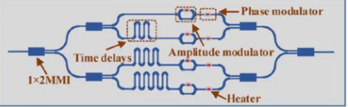
The principle of the filter is based on a four-tap FIR structure. The pattern structure is monolithically integrated on an SOI wafer, with the advantages of easy fabrication and compact footprint. The filter architecture is shown in Fig. 1. The input signal is divided into four taps by cascaded multimode interference (MMI) couplers, and then propagates through the four taps with a series of time delays. An amplitude modulation unit (realized by a Mach-Zehnder interferometer (MZI) with one arm phase-modulated) and a phase modulation unit are present on each tap. All phase modulation units are controlled by thermal electrodes. It is known that the refractive index of silicon varies with temperature, leading to the required change of phase. Thus, heating the waveguides can implement phase modulation. Implementing such a phase modulation unit in one arm of an MZI can further realize amplitude modulation.
Fig. 1. Schematic diagram of the proposed integrated programmable filter.
Assuming that the amplitudes and phases of the four taps are α1, α2, α3, α4 and φ1, φ2, φ3,
φ4, respectively, and the time delay between two adjacent taps is τ, the transfer function of the
optical filter can be expressed as [25]
( )
4 ( ) 0 1 = j n n n n H ω α e ωτ φ+ =∑
(1)where ω is angular frequency of light. Equation (1) indicates that the output spectrum can be reshaped by modifying the relative amplitude weights and phase shifts of the four taps. Assuming that the relative time delay between two consecutive taps is 10 ps, a programmable filter can be obtained with a free spectral range (FSR) of 100 GHz.
2.1. Central wavelength-tunable filter
Fig. 2. (a) Simulated transfer functions of the filter with different ∆φ values of 0 (blue solid line), 0.167π (blue dotted line), 0.286π (red solid line) and 0.87π (red dotted line), respectively, (b) Simulated transfer functions of the filter with bandwidth tunability. The 3dB bandwidths of case 1, case 2 and case 3 are 0.61 nm, 0.38 nm and 0.31 nm, respectively.
In order to tune the central wavelength of the filter but keep the filter shape unchanged, we can add constant phase shifts between consecutive taps, which is referred to as a complex-coefficient filter. Assuming that the phase difference between two adjacent taps is changed by
( )
4 ( ) 4 4 [ ]( )
0 1 1 1 = n n n j n j n j n n n n n n n H e e e H ϕ τ ω φ ωτ ϕ φ τ ω τ φ ϕ ω α α α ω ∆ + + +∆ + ′ + ∆ = = = ′ = = =∑
∑
∑
(2)whereω ω′ = + ∆ϕ τ . From Eq. (2), we can see that the shape of the filter remains the same and that the central frequency of the filter is shifted by∆ϕ τ . Figure 2(a) illustrate the spectral shift for different values of ∆φ. For example, the initial amplitude array and phase array for the four taps are set as α = [0.05, 1, 0.8, 0.225] and φ= [0.1π, 0.9π, 0.25π, −0.25π], respectively. When the phase step Δφ is 0 (blue solid line), 0.167π (blue dotted line), 0.286π (red solid line) and 0.87π (red dotted line), respectively, we can see that the central wavelength has been shifted by 0.065 nm, 0.115 nm and 0.345 nm, respectively. The maximum tuning range of central wavelength can reach the FSR of the filter if ∆φ = 2π.
2.2. Bandwidth tunable filter
A bandwidth-tunable filter can be achieved by jointly controlling both amplitude and phase arrays for all taps. Figure 2(b) shows an example of the bandwidth tunability by optimizing all amplitudes and phases of all taps. The amplitude array and phase array of the initial condition (named Case 1) are α = [0.05, 1, 0.8, 0.225] and φ= [0.1π, 0.9π, 0.25π, −0.25π], respectively. Then in Case2 we set the amplitude array and phase array to α = [0.039, 1, 0.63, 0.12] and φ= [0.86π, −0.035π, −0.85π, 0.67π], respectively, and in Case3 to α = [0.27, 0.77, 0.75, 0.25] and φ= [0.25π, −0.85π, −1.71π, −0.58π], respectively. As shown in Fig. 2(b), the FSRs of all cases are 0.8 nm i.e., 100GHz, and the 3dB-bandwidths of Case 1, Case 2 and Case 3 are 0.61 nm, 0.38 nm and 0.31 nm, respectively. That is to say, the tuning range of the bandwidth, defined as the maximum bandwidth minus the minimum bandwidth and then divided by FSR, can be at least 37.5% of the FSR, while the central wavelength remains fixed. It should be noted that wider tuning range can be obtained by choosing more amplitude and phase arrays. And when we set the amplitude array and phase array to α = [1,1,1,1] and φ = [0, 0, 0, 0], the 3dB-bandwidth of our filter is narrowest, i.e., 0.247 nm. So the bandwidth tuning range of our filter is 69.1% of FSR.
2.3. Shape-variable filter
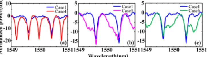
Fig. 3. Simulated transfer function of the filter with variable passband shapes. (a) The FSR of the filter is reduced to half of the original one (the amplitude array and phase array of Case4 are [0.8, 0.15, 0.8, 0.225] and [π, 0.99π, 0.207π, 0.248π], respectively), (b) and (c) Ramp-shaped transfer functions (the amplitude arrays and phase arrays of Case5 and Case6 are [0.6, 0.75, 0.5, 0.25], [-0.167π, 0.67π, 1.33π, 0] and [0.85, 1, 0.5, 0.25], [0.25π, −0.455π, 0.91π, −0.63π], respectively).
Our filter can be programmed to implement variable passband shapes as well. To fulfil a target filter, one needs to optimize and calculate the amplitude array and phase array of all taps so that the spectral response resembles the target filter as much as possible. For example, Fig. 3 shows some special filter shapes when varying the phase and amplitude arrays. In Fig. 3(a), the FSR of the filter (named as Case 4) becomes half of the original case (Case 1). In Case 4, the amplitude array and phase array are set as α = [0.8, 0.15, 0.8, 0.225] and φ= [π, 0.99π, 0.207π, 0.248π], respectively. In Figs. 3(b) and (c), we design ramp filters with descending and ascending characteristics, respectively. The amplitude and phase arrays
(Case 5 and Case 6) are α = [0.6, 0.75, 0.5, 0.25], φ = [-0.167π, 0.67π, 1.33π, 0] and α = [0.85, 1, 0.5, 0.25], φ= [0.25π, −0.455π, 0.91π, −0.63π], respectively.
3. Experimental verification
The design layout of the fabricated programmable filter is shown in Fig. 4. The filter was fabricated on an SOI wafer with 250 nm thick top silicon layer and 3 μm thick buried oxide (BOX). The height of the waveguide is 250 nm and the relative time delay of the four taps is 10 ps. The bending radius of the waveguide is 20μm. The size of our filter is about 2 mm2.
Fully etched apodized grating couplers [26] were used as input and output ports. A single step of E-beam lithography and inductively coupled plasma reactive ion etching (ICP-RIE) was used to fabricate the grating couplers and silicon waveguides, simultaneously. Then a 700 nm thick silica was deposited on the sample. Another layer of 700 nm bro-phospho-silicate-glass (BPSG) was deposited annealed in nitrogen condition in order to planarize the surface. After that, the top glass layer was thinned to 1μm by buffered hydrofluoric acid (BHF) etching. Finally, heater patterns (100 nm Ti) were formed by e-beam lithography followed by metal deposition and lift-off.
Fig. 4. Metallurgical microscopy image of the programmable filter.
In order to characterize our on-chip filter, light from a broadband optical source was coupled to the silicon chip with a vertical grating coupler. Because of the polarization sensitivity of the couplers and waveguides, a polarization controller (PC) was placed before the input grating coupler. The electrodes of the amplitude and phase arrays were contacted by a probe pin array spaced with 250 μm. Variable voltages generated from independent power supplies were applied to different pins in the array. Finally the output spectrum is measured by a high resolution (0.02 nm) optical spectrum analyzer (YOKOGAWA AQ6370C).
Fig. 5. (a) Measured transfer functions of the filter with different voltages on the phase electrode, which match well with the simulated ones in Fig. 2(a), (b) measured spectra of the filter with bandwidth tunability, the 3dB bandwidth of case1, case2 and case3 are 0.61 nm, 0.34 nm and 0.21 nm, respectively.
The loss of our filter is 9 dB when there is no voltages applied to the electrodes. And the loss of the coupling from the grating to fiber is about 11dB for both sides. Figure 5(a) demonstrates the tunability of the central wavelength of the filter transfer function. First, we adjusted all the voltages applied on the amplitude electrodes and phase electrodes so that the filter shape matches well Case 1. The output spectrum is shown as the blue solid line. The FSR of the filter is about 0.8 nm (i.e., 100 GHz). Then, all the voltages applied to the amplitude electrodes remained fixed, and the voltages applied to the phase electrodes were adjusted. The adjustment criterion is to keep the spectral shape unchanged, but to shift the
resonant wavelength. Finally we observed the wavelength shifts as shown in Fig. 5(a). The spectral shifts are about 0.06 nm, 0.1 nm and 0.34 nm, which match well with the simulated ones in Fig. 2(a).
Figure 5(b) shows measured transfer functions demonstrating bandwidth tunability by adjusting the voltages controlling both amplitude and phase arrays. The measured spectra are in good qualitative agreement with the calculation results shown in Fig. 2(b) for Case1, Case2 and Case3, respectively. The measured 3 dB bandwidths are 0.61 nm, 0.34 nm and 0.21 nm, respectively. We can see the maximum bandwidth tuning range of our filter is 0.4 nm, which is half of the filter’s FSR.
In order to demonstrate the variable shape filters, we tune the amplitude array and phase array to synthesize the special transfer function shapes corresponding to Case 4, Case 5 and Case 6. The measured spectra are shown in Fig. 6. In Fig. 6(a) the wavelength separations between adjacent resonant notches are 0.37 nm and 0.43 nm for Case 4 in one FSR, respectively, which has a slight difference from half of FSR (0.4 nm). In Figs. 6(b) and 6(c), we obtain descending and ascending ramp filters, in good agreement with the simulated results in Figs. 2(b) and 2(c), respectively.
Fig. 6. Measured transfer functions for shape-variable filters. (a) The FSR of the filter is reduced to half of the original one. (b) and (c) Ramp-shaped transfer functions.
The power consumption varies when the filter is in different functions, and the maximum power consumption is about 100 mW. The spectrum of the programmable filter is periodical due to the four-tap FIR structure. The FSR of the filter is inversely proportional to the time delay τ. Thus we can increase the FSR thereafter increase the filter tuning range by decreasing the time delay. For example, when τ = 10 ps, the FSR is 0.8 nm, and the maximum theoretical tuning range of central wavelength is about 0.8 nm. The situation is changed when τ = 2.5 ps. The FSR and tuning range are 3.2 nm, four time as large as in the case of τ = 10 ps. Comparing the measured transfer functions with the simulated ones, some deviations appear, which result from the non-uniform thermal conductivity of each electrode and device fabrication imperfections. To mitigate the impact of thermal non-uniformities, we can separate the thermal electrodes and waveguides over a larger region to prevent unwanted thermal diffusion. Besides, the number of taps influences the filter’s characteristics as well. We can obtain more elaborate filter transfer functions by fabricating FIR structures with eight or more taps.
4. Conclusions
We have proposed and demonstrated an on-chip programmable filter based on a four-tap FIR structure. By adjusting the voltages to control the amplitude and phase of taps, we have implement a filter with central wavelength, bandwidth and passband shape tunability. The central wavelength tunability is realized by adjusting the phase electrodes. The bandwidth tunability and variable passband shape are implemented by adjusting both the amplitude and phase electrodes. Our scheme has distinct advantages of compactness as well as capability for integration with electronics.
Acknowledgments
This work was partially supported by the National Natural Science Foundation of China (Grant No. 11174096 and 61475052), and the Danish Council for Independent Research (DFF–1337-00152 and DFF–1335-00771).
![Fig. 3. Simulated transfer function of the filter with variable passband shapes. (a) The FSR of the filter is reduced to half of the original one (the amplitude array and phase array of Case4 are [0.8, 0.15, 0.8, 0.225] and [π, 0.99π, 0.207π, 0.](https://thumb-eu.123doks.com/thumbv2/123doknet/12506517.340749/5.918.229.720.110.158/simulated-transfer-function-variable-passband-reduced-original-amplitude.webp)