1
Investigation of CVD multilayered graphene as negative electrode for
lithium-ion batteries
Mathieu Saulniera, Charles Trudeaub, Sylvain G. Cloutierb, Steen B. Schougaarda*
a NanoQam and Université du Québec à Montréal, Case postale 8888, Succ. Centre-ville, Montréal, Québec H3C 3P8, Canada
bDepartment of Electrical Engineering, École de technologie supérieure, 1100 rue Notre-Dame Ouest, Montréal, Québec, H3C 1K3, Canada
* Corresponding author E-mail address: [email protected] (S.B. Schougaard). First author E-mail address: [email protected]
Second author E-mail address: [email protected] Third author E-mail address: [email protected]
Abstract
Multilayered graphene (MLG) grown by chemical vapor deposition (CVD) was examined as a negative electrode for lithium-ion batteries. Experimental parameters such as deposition time and temperature were examined to produce carbon loadings between 0.06 – 0.17 mg cm -2 and film thicknesses in the 1µm range. The MLG thin films obtained on nickel substrate were used without conductive additive and binding agent in electrochemical tests to produce a capacity of ~250 mAh.g-1 at the 5C rate. Films were further characterized by scanning
electron microscopy, atomic force microscopy, grazing angle X-ray diffraction, X-ray photoelectron spectroscopy and Raman micro-spectroscopy mapping. By correlating the structural analysis to the electrochemical properties the importance of edge plane accessibility is emphasized. Separately, a pre and a post deposition treatment were used to improve the electrochemical performances, validating the structural performance limitation hypothesis.
2 Especially argon plasma post treatment showing major electrochemical improvement due to enhance accessibility to the edge access of the MLG films.
1. Introduction:
The increasing global energy demand causes depletion of the non-renewable energy sources such as petroleum, natural gas and coal.[1-3] Consequently, there is a growing interest in alternatives like wind and solar. However, efficient exploitation of these, especially for private transportation, is a considerable challenge. A similar issue was experienced for small electronic devices in the late 1980’s, which was addressed with the introduction of the lithium-ion battery.[4] More recently, lithium-ion batteries have found use in the hybrid and electric vehicle industry, but the available charging speed is limiting energy recovery during regenerative braking. [5] Similarly, batteries that can be imbedded directly in micro-devices are attracting increasing attention to improve autonomy and protection from unstable power sources.[6]
Carbonaceous materials such as graphite have been widely studied and applied as intercalation compounds for the negative electrode in lithium-ion batteries.[7-14] This is mainly due to large natural abundance of carbon, low price, good theoretical capacity (370 mAh.g-1), excellent cyclability and low Li-insertion potential due to weak binding of lithium to sp2 carbon-carbon bonds. Moreover, the small volume change between the charged and discharged material, as well as the high mobility of the electrons and lithium ions lead to fast diffusion. Because of these exceptional properties there is still considerable interest in
developing carbonaceous materials.
In recent years, the graphene sheets that makeup graphite have been produced individually while conserving intrinsic properties like high electric conductivity and electrochemical
3 stability. These materials may serve as negative electrodes, where lithium ions can be stored on both sides of the graphene sheets to yield an exceptional theoretical capacity of 740 mAh.g-1.[15] This theoretical capacity may however be difficult to reach at high rates, due to the low density of the composite electrode which significantly increases the electrolyte transport distance. (Supplementary material Table S1) More recently, a number of research papers have been reporting on a more densely stacked form of graphene, known as
multilayered graphene (MLG).[14, 16-18] MLG crystallites are made up of 2-10 layers of graphene stacked turbostratically. As such, these structures are intermediate between the purely 2D structure of graphene and the 3D structure of graphite, which in theory yields the possibility of augmenting density of the films while conserving some of the capacity
improvements of graphene vs graphite. To the best of our knowledge no previous research paper has evaluated µm thick MLG film for use as negative electrodes in lithium-ion batteries. (An non-exhausting overview of “graphene” based negative electrodes studies is available in Supplementary material Table S1)
To maximise the volumetric and the gravimetric energy densities of the battery, it is imperative to minimise the weight of the inactive materials. Consequently, in this work we report on the synthesis of MLG thin films directly atop the current collector without binder or conductive carbon. To this end of chemical vapour deposition (CVD) using ethylene as carbon precursor is chosen. This is because CVD is a) an industrially scalable technique, b) is well suited for producing thin film-batteries using roll-to-roll technology, and c) is a non-line of sight technique that can coat complicated shapes used in micro-batteries.
In this paper, the battery performance of MLG film was studied by correlating the deposition time (20 min; 40 min; 60 min; 80 min; 100 min), the temperature (700 ˚C; 800 ˚C; 900 ˚C; 1000 ˚C), the NiO reduction time and temperature before deposition, as well as argon plasma
4 post-treatment with the electrochemical profile, morphology, chemical composition and crystal structure.
2. Experimental
1.5 cm2 metallic nickel foil disks (30 µm thick, ≥ 99 % purity, MTI Corporation) were washed with water followed by acetone using sonication to eliminate soluble surface
impurities prior to carbon growth. These nickel substrates were placed in the middle of a gas tight 1.2 m long, 7.62 cm diameter quartz tube within a horizontal furnace (HT-OTF-1200X, MTI Corporation). Before heating, the reductive gas (5 % H2 in Argon, Praxair) was passed through the quartz tube at 1000 sccm for 30 minutes to remove ambient air. The reducing gas was kept constant at 1000 sccm during the heating procedure: room temperature to 1000˚C in 60 min.; maintained for 60 min.; decreases at 5˚Cmin-1 to the chosen synthesis temperature; maintained during deposition and cooled down to room temperature without temperature control. The carbon precursor gas (Ethylene 99.9 % purity, Praxair) was added to the
reductive gas only during deposition at a flow of 25 sccm. Argon plasma post-treatment was done at 240 Watts for 15 minutes under a flow of 20 sccm (Diener Electronic, PICO) on selected samples. Carbon loading was determined by subtracting the sample mass before deposition from the mass after deposition.
The morphology was examined with a JEOL JSM840 SEM using a backscattering detector and 15.0 kV acceleration voltage, a Veeco/Bruker Multimode AFM in contact mode (mapping 100 µm X 100 µm) and an optical microscope (WITec Alpha 300R Confocal Raman Imaging System). Grazing angle X-ray diffraction was obtained with a CuKα source Philips X’pert diffractometer (2ϴ = 20˚- 30˚), Raman spectral maps with a WITec Alpha 300R Confocal Raman Imaging System equipped with a 532 nm excitation laser, (mapping 100 µm x100 µm), and X-ray photoelectron spectroscopy (XPS) with Physical Electronics
5 XPS PHI 5600-ci spectrometer using a Al-Kα (1486.6 eV) 300W for survey scans and Mg-Kα (1253.6 eV) at 150 W for high resolution spectra.
Coin cell batteries were prepared in an argon atmosphere glovebox (water and O2 content < 1 ppm) using the “as produced” MLG sample, Celgard 2500 membranes as separator and 0.75 mm thick metallic lithium (Sigma-Aldrich). 1M LiPF6 in EC:DMC (1:1) (water: 4.0 ppm, HF: 35.8 ppm) or 1M LiClO4 in EC:DMC (1:1) (water 25.7 ppm) were used as electrolytes
(BASF). The geometrical areas for the electrodes were 1.5 cm2 and 2.0 cm2 for the carbon and lithium electrode respectively. Electrochemical testing was performed by galvanostatic
cycling (0.005-2.0 V vs Li/Li+) at room temperature using a BST8-MA battery analyser. A 30 min. open circuit rest period was imposed to the batteries after every charge and discharge step. Imposed rates are cited in hours needed for complete charge, e.g. a C/10 rate provides the current to fully charge the material in 10 hours and a 5C rate in 12 minutes. The
galvanostatic currents required to this end were determined by multiplying the experimental MLG films mass with the theoretical capacity of LiC6 (370 mAh.g-1) and dividing by the desired time for full charge.
3. Results and Discussion:
3.1.
Effect of Electrolyte, Synthesis Temperature and Deposition Time on
Galvanostatic Performance
MLG films from a single deposition run (700 ˚C / 20 min.) were used in coin cell batteries with two different electrolytes. (1M LiPF6 and 1M LiClO4 in EC:DMC (1:1)) Comparing the galvanostatic measurements at different C rates, shows that the reaction kinetics is
6 (Supplementary material Figure S1). This phenomenon is not fully understood yet, but could be attributed to the intricacies of formation of the solid electrolyte interface (SEI) layer.[19-21] Studying SEI formation is beyond the scope of this work. Consequently, the LiClO4 electrolyte was utilized for all further preparations.
Figure 1
Films deposited at 700 ˚C with varied deposition time show discharge capacities close to 370 mAh.g-1 at slow speed (C/10) i.e. the theoretical capacity for LiC6. As the cycling speed increases, only the 20 minutes deposition sample retains most of the initial capacity. The four other samples decrease rapidly until no capacity remains at 5C.
Examining the discharge capacities as a function of deposition temperatures shows again at low speed (C/10) values close to the 370 mAh.g-1 theoretical capacity (Figure 1B). Similarly to the results presented in Figure 1A, a capacity decrease is observed as the current is
increased, however this decrease is less drastic. From an electrochemical perspective this begs the question why the 20 min. deposition samples are so singularly different and why samples deposited at higher temperatures show better performances at intermediate current densities. In an attempt to derive a response and provide ideas to improve the electrochemical
performance, extensive analysis of loading, morphology, electrochemical profile and the atomic structure was performed.
3.2. Multilayered Graphene Loading and Morphology
Multiple factors cause variations of the quality, thickness, density and morphology of CVD MLG materials on a metallic substrate. In order to evaluate only the impact of deposition time and synthesis temperature on the electrochemical performance, parameters such as: gas flow, surface treatment, type of metallic substrate and cooling procedure were kept constant.
7 Metallic nickel was chosen here as substrate because of its catalytic properties for CVD carbon deposition at low temperature. [11, 16, 22-27]
Figure 2
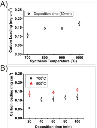
Figure 2A shows the evolution of MLG loading on the nickel substrate using different
synthesis temperatures and 60 min. deposition. Importantly, the carbon loading increases with the increased temperature. Figure 2B shows that the carbon growth rate is significantly
reduced after 40 min. at 700 ˚C whereas this reduction in rate has already taken place after 20min. at 900 ˚C. This suggests that the substrate surface is still exposed, or at least still catalytically active for up to 40 min at 700 ˚C, after which catalysis is attenuated. A common model for carbon film growth on nickel involves three growth steps, where the first step is the decomposition of the carbon precursor at the surface of the substrate, followed by dissolution of carbon in the nickel “bulk” and finally formation of the film as carbon is transported to the surface when the solubility limit is reached during cooling.[11, 23, 25, 28] However, the measured carbon film mass compared with the solubility and diffusion coefficient of carbon in nickel provided by Lander et al.[29], indicate that the mass loading is higher than the carbon solubility limit for all the depositions in this work.(Supplementary material Equations S1, S2, S3 and Figure S2 and S3) The dominant growth mode must therefore be different.
Figure 3
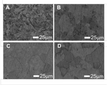
The contrast of the 700 ˚C, 20 min. deposition SEM micrograph (Figure 3A) suggest that the “ocean” which has higher backscattered electron emission is covered by a carbon film with lower thickness compared to the “islands”. This observation was confirmed by AFM (See Supplementary material Figure S4 and Table S2) and is consistent with preferential growth of multilayered graphene at grain boundaries for polycrystalline nickel films.[11, 22, 23, 25, 27] For all other films presented in Figure 3, the surfaces show more uniform backscattered
8 electron intensity and therefore similar carbon thicknesses. The “cracks” between the platelets suggest that carbon grows from the “islands seed” until they converge to form a rift between them. The SEM micrographs explains the carbon loading evolution as the carbon growth decreases significantly or stops once the surface is fully covered due to the lack of the catalytic effect of exposed nickel. The effect of temperature was also examined for 60 min. deposition time. Here the fully-covered films did not show a significant morphological difference consistent with the model that once the surface is covered all reaction is significantly slowed or halted (Supplementary material Figure S5 and Table S3).
3.3. Atomic Level Structure
3.3.1. X-Ray Diffraction
Graphitic carbon structure is composed of multiple sp2 carbon graphene sheets held together by weak van der Walls interactions. This configuration permits the intercalation and
stabilisation of lithium ions between two layers of graphene. The graphite unit cell (P63 /
mmc) shows a sheet-to-sheet distance of 3.354 Å at room temperature.[7] As such, the
diffraction peak between 25 and 30 degrees, which was the only one with sufficient intensity to be considered for analysis, originate from the (002) planes. Three structural parameters can be determined with the XRD data. First, using the diffracted peak 2ϴ angle and the Bragg equation the d-spacing can be evaluated. (Supplementary material Equation S4). Secondly, with the same angle and the peak full-with-at-half-maximum (FWHM) and the Scherrer equation crystallite size in the c-direction was calculated (Supplementary material Equation S5). The final parameter is obtained by dividing the crystallite size with the d002 i.e the graphene to graphene sheet spacing yields the average number of graphene layers per
crystallite. (Supplementary material Equation S6) All experimental and calculated values are presented in the Supplementary material, Table S4.
9 Figure 4
The d-spacing (Figure 4A, B) remains uniform throughout and within 0.4 % of the literature values.[7, 8] Similarly, crystallite size is unaffected by the deposition conditions, except for 1000 ˚C / 60 min., where a significant increase is observed. Consequently, the number of layers per crystallite has significantly increased at the maximum temperature studied. As the mass per area is only marginally affected by the increase in temperature, this suggests that 1000 ˚C / 60 min. deposition leads to higher order, consistent with higher deposition
temperatures leading to higher mobilities of intermediate species and thus greater probabilities of reaching the thermodynamically lowest energy state. Importantly the number of layers in the structures is between 3 and 6 layers, meaning that the carbon films thickness is composed of many crystallites of graphene. In fact, according to the carbon loading of the structures and the theoretical specific surface value of graphene (2600 m2g-1) [8], the number of layers would be between 1300 and 5200 rather than 3 to 6, if the carbon was perfectly organised on the surface of the nickel substrate.
3.3.2. X-Ray Photoelectron Spectroscopy
The chemical composition of the sample surface was examined by XPS. Survey scans reveals the presence of C (1s) and O (1s) without indication of a significant signal for other elements. Specifically, the Ni 2p signal around 853 eV was absent, indicating that the nickel surfaces are fully-covered with a film thicker than the escape depth of the photoelectron. The oxygen concentration was found to be at 4-7 %. (Supplementary material Table S5) High resolution scans and deconvolution of the peaks for C (1s) were executed to obtain information on the nature of the oxygen bonding. The results reveal that the major peak component is the C=C bond at 284.5 eV, followed by two oxygen related peaks C-OH at 285.4 eV and C-O-C at 286.2 eV. Little or no intensity was found at 287.4 eV and 289.4 eV suggesting the absence
10 of carboxylic or ketone functions at the film surface. The presence of oxygen is expected in MLG films due to a high number of edge planes accessible.[30, 31] These terminal carbons are easily oxidized in presence of ambient air between the synthesis and battery fabrication steps. The π-π* satellite peak at 291.5 eV is visible in the majority of the films, originating from a strong delocalization of electrons characteristic of graphene-like materials.[32] All spectra and their deconvolutions are available in the supplementary material. (Supplementary material Figure S6)
3.3.3. Raman Micro-Spectroscopy
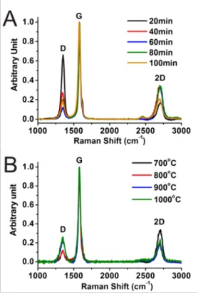
Raman micro-spectroscopy provides crucial information on carbon bonding within the film. Three major peaks, D, G and 2D are observed. The D peak around 1360 cm-1 is associated with the breathing modes of the 6 members sp2 carbon ring which is only Raman active when proximity to sp3 carbon defect or edge breaks symmetry.[33-36] Consequently, high purity graphene does not lead to a D peak due to the large crystallite size and therefore low relative edge carbon concentration, whereas our MLG exhibit a significant D signal due to a
significant defect and edge carbon concentration. The second peak near 1580 cm-1
corresponds to the E2g phonon is labelled G or so-called “G-band”.[33-36] Its activity is due to the symmetric and antisymmetric stretching modes between sp2 carbon. The I
D/IG ratio is utilized to compare the relative amount of sp2 carbon to sp3 carbon and edges, between different structures. The last major peak situated around 2700 cm-1 is the second-order resonance of the D peak or so-called 2D-band. [33-36] This vibration is activated by the combination of two phonons with opposite wave vectors and is therefore Raman active even when defects are not present. [36] The shape and position of the 2D peak is affected by the number of graphene sheets in the film. [33, 36] Consequently, it is possible to quantify
11 between 1 and 5 layers (higher than 5 will be considered graphite) as function of the peak position.
Figure 5
Raman spectra average of the 100 µm by 100 µm maps (Figure 5) shows that the ID/IG ratio is largest for 20 minutes deposition at 700˚C. Similarly, mapping shows a strongly
inhomogeneous film with strong Raman intensity variations, especially near and around the edges of the carbon ‘’islands’’ (See Supplementary material Figure S4 and Table S2). Increasing the deposition time leads to a decrease of the ID/IG ratio with a minimum at 700 ˚C/60 min. The frequency of the 2D peak maxima suggests ordered domains of 3-5 layers similar to the diffraction analysis for all samples with a deposition time higher than 20 min. The data confirms that significantly more defects or edges are present in the sample at 700 ˚C / 20 min.
3.4. Electrochemical Profiles
During lithium intercalation and deintercalation in graphite, the potential profile has tree distinctive plateaus at ≈ 210 mv, ≈120 mV and ≈90 mV vs Li/Li+.[7, 37] The plateaus are a consequence of thermodynamics as the sample converts from one structural distinct phase, with a fixed lithium concentration to another.[7, 37] The absence of a distinct plateau
indicates that a) the insertion mechanism is kinetically limited due to slowed Li+ transport or increased electronic resistance yielding non-uniform electrochemical potential within the film coating, b) the amount of defects prohibits formation of phases with distinct lithium contents, and/or c) that the charge storage mechanism resembles that of a graphene, i.e. is based on double layer capacity rather than charge transfer. [7, 37] MLG films display two distinctive potential profiles depending of synthesis parameters (Figure 6 A).
12 Figure 6
The graphite type electrochemical profile is found in the 700˚C / 20 min. ; 800˚C / 60 min. ; 900˚C / 60 min. and 1000˚C / 60 min. MLG films. Therefore, these samples are less limited by charge transport. The capacity does not decay exponentially as the current density is increased (Figure 1), which suggests a predominately resistive limitation process. Contrarily, an absence of plateau in the galvanostatic curves is found for the 700˚C / 40 min.; 700˚C / 60 min. ; 700˚C / 80 min. and 700˚C / 100 min. MLG films. In addition an overpotential increase between the charge and discharge curve by a factor ~4 is observed (Figure 6 A), consistent with the rapid decay of the capacity (Figure 1). Similarly, examining the crossover position for the charge and discharge curves to estimate the overpotential (Supplementary Material Figure S7) we find (Figure 6 B) as expected that the 700˚C / 20 min. sample exhibit a relative capacity crossover close to the zero overpotential value of 50 % (49 %) i.e. little or no Ohmic resistance and/or concentration limitation. As for all other samples a shift from 50% occurs, with an amplitude that correlates with the capacity decay. Importantly, the ID/IG ratio of RAMAN spectroscopy does not seem to be a strong indicator for performance when comparing all samples, as we find that samples with widely different performance may exhibit quite similar spectra (Figure 5b, 700-800˚C / 60min). This may be due to the limited probing depth of the spectroscopy or to the inability of probing with sufficient detail the geometry and chemical composition of the “cracks” between the MLG “islands”. Similarly, the thickness of the SEI layer as indicated by the five first cycles irreversible capacities does not appear as a strong indicator of performance in the studied films (Supplementary material Figure S8) From comparison of the SEM and AFM data to the electrochemistry, it is clear that the space between the “island” MLG has a profound effect on the negative electrode
performance. Similarly, regions with high defect concentrations showed improved electron transfer kinetics in previous studies of highly ordered “few-layered” graphene.[38-41]
13 Therefore, in an attempt to improve the electrochemical performance in thicker films studied here, a pre and a post deposition treatment technique is evaluated in the next section.
3.5. Pre and Post-Treatment of MLG Thin Films Deposition
3.5.1. Effect of Nickel Oxide Reduction Time Pre-Treatment
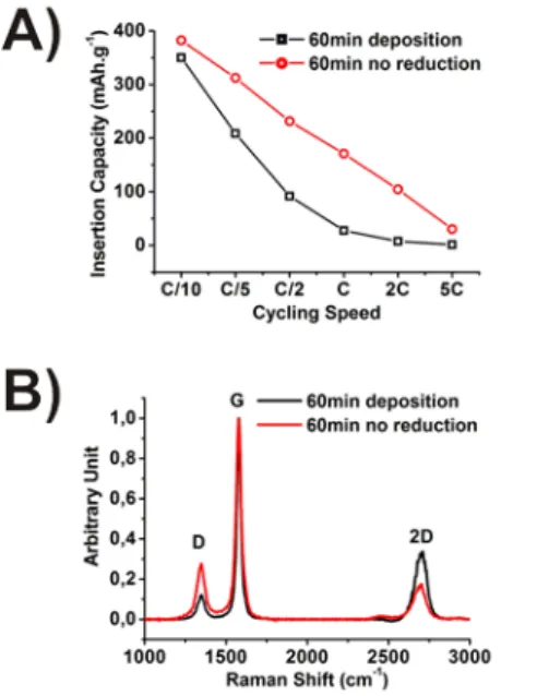
It has been established that the catalytic activities and grain size of the metallic nickel are correlated, i.e. grain boundaries are believed to catalyze carbon deposition on the nickel substrate.[11, 22, 25, 28] Consequently, to obtain efficient carbon growth it would in theory be imperative that the nickel oxide layer has been reduced before introducing the carbon precursor. The experimental protocol in this study reduces the oxide by exposure to 5 % H2 in argon for 60 minutes at 1000˚C before deposition. Using similar environment even at lower temperatures proves effective in reducing the oxide.[42, 43] Another effect of heating at 1000˚C is the enlargement of the crystal grain size in the metallic nickel. For a series of samples at 700˚C with a deposition time of 60 minutes, the reducing step at 1000˚C was removed from the heating protocol. The SEM micrographs (Supplementary material Figure S9) illustrate the increase in film “crack” density when no 1000˚C reduction treatment is used. In addition, the Raman mapping (Supplementary material Figure S9 and Table S6) and
average spectra (Figure 7 B) show an increase of ID/IG ratio signal when compared to carbon film deposited after the 1000˚C reduction step. Moreover, the galvanostatic measurements presented in Figure 7A, show improved electrochemical performance for all cycling speeds. Consequently, removal of the NiO reduction step has a direct effect on the electrochemical results for the MLG films and confirms the importance of grain size and boundaries as detailed above.
14
3.5.2. Effect of Argon Plasma Post-Treatment
To evaluate the accessibility of lithium ions through defects or cracks in the film layer, plasma post-treatment was performed. Similarly, Güell et al. have shown that argon plasma treatment creates defects on graphene films.[39] The Raman average spectra (Figure 8B) reveal the plasma’s effectiveness in this regard as the D/G ratio is significantly increased for the treated MLG film. The effect at low rates on capacity is minimal since theoretical capacity had already been reached in the untreated samples, however, at higher rates a significant augmentation of the discharge capacity is found (Figure 8A). The plasma induced defect must however be of limited size as SEM micrographs of the sample before and after plasma
treatment (Figure S7) shows no significant morphological differences i.e. the plasma treated MLG film does not reveal more cracks than the non-treated MLG film.
Figure 8
4. Conclusion
Decreasing weight and volume as well as adding malleability to lithium-ion cells are all key factors to the battery industry. Improving thin film batteries would enable advancements in small device and high-rate applications. In this work we have shown fabrication of thin MLG films that can be used as negative electrode in lithium-ion batteries without addition of
conducting additive and binder. We were able to obtain a capacity of 250 mAh.g-1 at a 5C rate for µm thick electrodes. Further, it was demonstrated that accessibility of the edge plane of the carbon is essential to facilitate Li+ diffusion in the structure. As such, a clear correlation
15 between morphological defects in the films and the discharge capacity retention at high speed was shown. Electrolyte selection, synthesis temperatures, deposition time, oxide reduction and an argon plasma post-treatment have been used to improve the performance of the materials in this work. In fact, argon post-treatment is clearly the most effective technique develop in this paper to increase the films specific power. Future work to improve edges accessibility using industrial relevant technologies could include mask patterning, induction of physical defects with harsh chemical post-treatment or inclusion of atomistic defects during the deposition (I2 or melamine)[44] and c-axis epitaxial growth from specialize substrates.
Acknowledgements
The authors thankfully acknowledge Dr. Gwenaël Chamoulaud from NanoQam for the technical support. The authors also gratefully acknowledge the National Science and
Engineering Research Council (NSERC) for financial support grant #326937-2013-RGPIN. The 25 µm microporous monolayer membrane (PP) was kindly donated by Celgard.
References
[1] M. Asif and T. Muneer Renewable and Sustainable Energy Reviews 2007, 11, 1388.
[2] J. P. Dorian, H. T. Franssen and D. R. Simbeck Energy Policy 2006, 34, 1984.
[3] Z. Huang, H. Yu, Z. Peng and M. Zhao Renewable and Sustainable Energy Reviews 2015, 42,
1335.
[4] Y. Nishi Journal of Power Sources 2001, 100, 101.
[5] M. Li, H. Xu, W. Li, Y. Liu, F. Li, Y. Hu and L. Liu Energy 2016, 112, 1273.
[6] Y. Yue and H. Liang Journal of Power Sources 2015, 284, 435.
[7] M. Inaba In Encyclopedia of Electrochemical Power Sources; G. Editor-in-Chief: Jürgen, Ed.; Elsevier: Amsterdam, 2009, p 198.
[8] N. A. Kaskhedikar and J. Maier Advanced Materials 2009, 21, 2664.
[9] Y. Kobayashi, S. Seki and N. Terada In Encyclopedia of Electrochemical Power Sources; G. Editor-in-Chief: Jürgen, Ed.; Elsevier: Amsterdam, 2009, p 375.
[10] A. Stein, Z. Wang and M. A. Fierke Advanced Materials 2009, 21, 265.
[11] Y. Zhang, L. Zhang and C. Zhou Accounts of Chemical Research 2013, 46, 2329.
[12] S. Goriparti, E. Miele, F. De Angelis, E. Di Fabrizio, R. Proietti Zaccaria and C. Capiglia Journal of Power Sources 2014, 257, 421.
[13] W. Sun and Y. Wang Nanoscale 2014, 6, 11528.
[14] X. H. Xia, D. L. Chao, Y. Q. Zhang, Z. X. Shen and H. J. Fan Nano Today 2015, 9, 785.
16 [16] P. Trinsoutrot, H. Vergnes and B. Caussat Materials Science and Engineering: B 2014, 179, 12.
[17] D. T. Oldfield, D. G. McCulloch, C. P. Huynh, K. Sears and S. C. Hawkins Carbon 2015, 94, 378.
[18] H. Sun, A. E. Del Rio Castillo, S. Monaco, A. Capasso, A. Ansaldo, M. Prato, D. A. Dinh, V. Pellegrini, B. Scrosati, L. Manna and F. Bonaccorso Journal of Materials Chemistry A 2016, 4, 6886.
[19] A. V. Plakhotnyk, L. Ernst and R. Schmutzler Journal of Fluorine Chemistry 2005, 126, 27.
[20] T. Kawamura, S. Okada and J.-i. Yamaki Journal of Power Sources 2006, 156, 547.
[21] R. Marom, O. Haik, D. Aurbach and I. C. Halalay Journal of The Electrochemical Society 2010,
157, A972.
[22] S. J. Chae, F. Güneş, K. K. Kim, E. S. Kim, G. H. Han, S. M. Kim, H.-J. Shin, S.-M. Yoon, J.-Y. Choi, M. H. Park, C. W. Yang, D. Pribat and Y. H. Lee Advanced Materials 2009, 21, 2328.
[23] A. Reina, S. Thiele, X. Jia, S. Bhaviripudi, M. Dresselhaus, J. Schaefer and J. Kong Nano Res.
2009, 2, 509.
[24] H. J. Park, J. Meyer, S. Roth and V. Skákalová Carbon 2010, 48, 1088.
[25] L. Baraton, Z. B. He, C. S. Lee, C. S. Cojocaru, M. Châtelet, J. L. Maurice, Y. H. Lee and D. Pribat EPL (Europhysics Letters) 2011, 96, 46003.
[26] H. Bi, F. Huang, J. Liang, Y. Tang, X. Lu, X. Xie and M. Jiang Journal of Materials Chemistry
2011, 21, 17366.
[27] W. Chen, Z. Fan, G. Zeng and Z. Lai Journal of Power Sources 2013, 225, 251.
[28] Q. Yu, J. Lian, S. Siriponglert, H. Li, Y. P. Chen and S.-S. Pei Applied Physics Letters 2008, 93.
[29] J. J. Lander, H. E. Kern and A. L. Beach Journal of Applied Physics 1952, 23, 1305.
[30] D. W. Boukhvalov and M. I. Katsnelson Journal of the American Chemical Society 2008, 130,
10697.
[31] L. Cardenas, J. MacLeod, J. Lipton-Duffin, D. G. Seifu, F. Popescu, M. Siaj, D. Mantovani and F. Rosei Nanoscale 2014, 6, 8664.
[32] M.-C. Hsiao, S.-H. Liao, M.-Y. Yen, C.-C. Teng, S.-H. Lee, N.-W. Pu, C.-A. Wang, Y. Sung, M.-D. Ger, C.-C. M. Ma and M.-H. Hsiao Journal of Materials Chemistry 2010, 20, 8496.
[33] A. C. Ferrari Solid State Communications 2007, 143, 47.
[34] I. Calizo, I. Bejenari, M. Rahman, G. Liu and A. A. Balandin Journal of Applied Physics 2009,
106, 043509.
[35] D. R. Lenski and M. S. Fuhrer Journal of Applied Physics 2011, 110, 013720.
[36] A. C. Ferrari and D. M. Basko Nat Nano 2013, 8, 235.
[37] T. Abe In Encyclopedia of Electrochemical Power Sources; G. Editor-in-Chief: Jürgen, Ed.; Elsevier: Amsterdam, 2009, p 192.
[38] D. A. C. Brownson, L. J. Munro, D. K. Kampouris and C. E. Banks RSC Advances 2011, 1, 978.
[39] A. G. Güell, A. S. Cuharuc, Y.-R. Kim, G. Zhang, S.-y. Tan, N. Ebejer and P. R. Unwin ACS Nano
2015, 9, 3558.
[40] Y. Zhan, B. Zhang, L. Cao, X. Wu, Z. Lin, X. Yu, X. Zhang, D. Zeng, F. Xie, W. Zhang, J. Chen and H. Meng Carbon 2015, 94, 1.
[41] J. Hui, M. Burgess, J. Zhang and J. Rodríguez-López ACS Nano 2016, 10, 4248.
[42] Q. Jeangros, T. W. Hansen, J. B. Wagner, C. D. Damsgaard, R. E. Dunin-Borkowski, C. Hébert, J. Van herle and A. Hessler-Wyser J Mater Sci 2013, 48, 2893.
[43] K. V. Manukyan, A. G. Avetisyan, C. E. Shuck, H. A. Chatilyan, S. Rouvimov, S. L. Kharatyan and A. S. Mukasyan The Journal of Physical Chemistry C 2015, 119, 16131.
[44] H. Liu, Y. Zhang, R. Li, X. Sun, S. Désilets, H. Abou-Rachid, M. Jaidann and L.-S. Lussier Carbon
17
Figures:
Figure 1: Insertion capacities as a function of A) deposition time at 700˚C and B) synthesis temperatures for 60 min. deposition in 1M LiClO4 in EC:DMC (1:1)
Figure 2: Carbon loading on nickel substrate as a function of A) synthesis temperature and B) deposition time
18 Figure 3: SEM micrographs of carbon films,700 ˚C / 20-40-60-80 min. (A-B-C-D)
Figure 4: d-spacing; crystallite size and # of layers of carbon films calculated from XRD diffractograms, A) 700 ˚C / 20-40-60-80-100 min. and B) 700-800-900-1000 ˚C / 60 min.
19 Figure 5: Raman spectra average from mapping A) 700 ˚C / 20-40-60-80-100 min. B) 700-800-900-1000 ˚C / 60 min
Figure 6: A) Insertion and deinsertion curves at a C/10 rate for 700˚C / 20 min deposition (in black) and 700˚C /40 min (in red). Single headed arrows show cycling sense and double headed arrow the difference of internal resistance between insertion and deinsertion curves. (Figure S6 for the full range electrochemical profiles) B) Relative capacity of charge discharge curve crossover vs deposition parameters
20 Figure 7: 700˚C / 60 min deposition with and without NiO reduction step A) Insertion capacities and B) Raman spectra average from mapping
Figure 8: 700˚C / 60 min. deposition with and without Ar plasma post-treatment A) Insertion capacities B) Raman spectra average from mapping