Democratic and Popular Republic of Algeria
Ministry of Higher Education and Scientific
Research
University Echahid Hamma Lakhdar-El Oued
Faculty of Technology
Department of Electrical engineering
Memory
Submitted in fulfillment of the requirements of the degree of
MASTER ACADEMIQUE
in Telecommunication
Entitled:
by: Oussama BENNACER
Examination committee:
Nacereddine Lakhdar
MCA
Supervisor
Medjouri Abdelkader
MCB
Chairman
Boukaous chahra
MCB
Examiner
May 2017
Study and modeling of submicron Triple
material gate GaAs MESFET
Dedication
I dedicate this work
To my parents, my wife, my brother, my sisters
To the whole family
To my friends
To you who helped me
With all my tenderness
Acknowledge
I thank Allah, the all-powerful, for teaching me what I did not know, for giving me health and everything I needed to do this work.
I thank my parents, and all my family for their encouragement.
I thank my supervisor Dr. Nacereddine Lakhdar for the theme he offered me, his advices and his availability.
I would of course like to thank the members of the jury who did me the honor to examine this work.
I thank my friends Nadjib, Mohammed Elhadi, Sifeddine , Belhadj, Tarek for helping me. I will conclude by thanking my dear colleagues and all the teachers of the department of Electrical engineering.
Abstract
The great technological development we have achieved requires more efficient, small-scale, and low-power components .In this memory, a new analytical model for a Triple Material Gate (TM) GaAs MESFET has been proposed in order to suppress the short channel effects and improve the electrical behavior of the device. Therefore, the aim of this work is to demonstrate the improved electrical performances exhibited by (TM) GaAs MESFET over dual material gate and conventional single material gate MESFET. This approach is based on development of I-V characteristics, transconductance and cut off frequency of TM GaAs MESFET. The model is further extended to evaluate the I-V characteristic, transconductance and cut-off frequency including the effect of third region length for microwave frequency applications. The obtained results demonstrate that TM GaAs MESFET presents an alternative solution to designer for high frequency applications.
Keywords: Triple-Material-gate, Modeling, GaAs-MESFETs, Short channel
Résumé
Le grand développement technologique que nous avons accompli nécessite des composants plus efficaces, à petite échelle et à faible puissance. Dans cette mémoire, un nouveau modèle analytique pour un GaAs MESFET de grille à Triple Matériaux (TM) a été proposé afin de supprimer les effets de canal courts et améliorer le comportement électrique de composant. Par conséquent, le but de ce travail est de démontrer les performances électriques améliorées présentées par (TM) GaAs MESFET par apport le GaAs MESFET de grille à double matériaux et le MESFET conventionnel de grille à un matériel unique. Cette approche est basée sur le développement des caractéristiques I-V, la transconductance et la fréquence de coupure de TM GaAs MESFET. Le modèle est encore étendu pour évaluer la caractéristique I-V, la transconductance et la fréquence de coupure, y compris l'effet de la troisième longueur de région pour les applications de fréquence micro-ondes. Les résultats obtenus démontrent que TM GaAs MESFET présente une solution alternative au concepteur pour les applications de haute fréquence.
Mots-clés: Triple-Matériaux-grille, Modélisation, GaAs-MESFETs, Effets de
خلم ص بلطتي هانققح يذلا ريبكلا يجولونكتلا روطتلا نإ رصانع ةءافك رثكأ امجح رغصأو .ةقاط ضفخأو ف يف لا هذه ةلاسر ديدج يليلحت جذومن حارتقا مت ، ل ـ GaAsMESFET داوملا ةيثلاث ةباوب وذ ، لجأ نم ضفخ آ ةانقلا راث نيسحتو ةريصقلا سزنارتلا ءادأ روت ايئابرهك تابثإ وه لمعلا اذه نم فدهلا نإف ،كلذلو . دأ نسحت ىدم ءا GaAs MESFET ةباوب وذ يثلاث ايئابرهك داوملا ة اضيأو ،داوملا ةيئانث ةباوبلا وذ هيريظن عم ةنراقم اعلا ةباوبب يأ يد .ةداملا ةيداحأ و ةبراقملا هذه دنتست ىلع ريوطت لا صئاصخ عطقلا ددرتو ةيئابرهكلا علل رصن GaAs MESFET وذ .داوملا ةيثلاث ةباوب اذه يف جذومنلا مييقت متي لا صئاصخ ةيئابرهكلا و ددرت عطقلا كلذكو لوط ريثأت ةثلاثلا ةقطنملا ةباوبلل لا لجأ نم تاقيبطت لا تاذ تاددرت ةيلاعلا نأ اهيلع لوصحلا مت يتلا جئاتنلا ترهظأ . GaAs MESFET وذ داوملا ةيثلاث ةباوب لاح مدقي ممصمل لايدب ي ا .ددرتلا ةيلاع تاقيبطتل :ةيحاتفم تاملك ،ميمصت ،داوملا ةيثلاث ةباوب GaAs MESFET ، ةريصقلا ةانقلا راثآ .عطقلا ددرت ،
Contents
Abstract List of figures Abbreviations
Introduction 1
Chapter I Study of the conventional structure of MESFET 3
1. Introduction 3 2. MESFET’s Overview 4 3. GaAs MESFET 5 4. MESFETs operation 6 5. MESFET characteristics 9 5.1 I-V characteristics 9
5.2 Transconductance & output conductance 10
5.3 Cut off frequency 11
6. Conclusion 12
Chapter II Study of DM GaAs MESFET-based design 13
1. Introduction 13
2. Device structure and Models formulation 14
3. Results and discussion 18
4. Conclusion 22
Chapter III Modeling of TM GaAs MESFET-based design 23
1. Introduction 23
2. Device structure and Models formulation 24
3. Results and discussion 29
4. Conclusion 33
Conclusion 34
List of figures
Figure I.1: Cross section of a GaAs MESFET device. 4 Figure I.2: Actual GaAs MESFET layouts: (a) interdigitated-gate, (b) π-gate. 6 Figure I.3: GaAs MESFET operation under different Vds biasing with Vgs ≤ 0:
(a) Linear region (Vds is very low), (b) Vds at the onset of saturation,
(c) Vds is big. 8
Figure I.4: I-V Characteristic curves for a MESFET device for different values of Vgs; ideal current is drawn in solid curve while dashed curve
indicates the actual current. 10
Figure II.1: (a) Cross-sectional view of the analyzed DM GaAs-MESFET (b)
equivalent circuit representation for a drain current modeling. 14 Figure II.2: Output characteristics for a channel length of a 0 .2 200µm2
(
L
1
0
.
1
µm
) DG GaAs-MESFET compared with that of theconventional SM GaAs-MESFET. 19
Figure II.3: variation of the saturation drain current,Idsat, as function of metal
gate work function near the drain end,
M2, for a fixedµm L and eV V V V Vgs 0 , ds 6 , M1 5.3 10.1 . 20
Figure II.4: (a) Variation of the transconductance as a function of increasing work function of the metal gate work function for a fixed
µm L and eV V V V Vgs 0.5 , ds 4 , M15.3 1 0.1 . (b) Variation of the output conductance with the increase in the work function of
the gate metal near the drain end. 21 Figure III.1: (a) Cross-sectional view of the analyzed TM GaAs MESFET. (b)
Equivalent circuit representation for a drain current modeling. 25 Figure III.2: Output characteristics for a channel length of 0.2 × 200 µm2 TM
GaAs MESFET compared with that of the SM and DM GaAs
MESFETs. 30
Figure III.3: Output characteristics for a channel length of 0.2 × 200 µm2 TM GaAs MESFET with deferent length of the third region for a fixed
Figure III.4: Variation of Transconductance with gate to source voltage for a channel length of 0.2 × 200 µm2 TM GaAs MESFET with deferent
length of the third region for a fixed Vds=5V 31
Figure III.5: Variation of cut-off frequency with drain to source voltage for a channel length of 0.2 × 200 µm2 TM GaAs MESFET with deferent
Abbreviations
a Epi-layer thickness FET Field Effect Transistor
ft Unity gain frequency
GaAs Gallium Arsenide
gd Output conductance gm Transconductance h Depletion width I-V Current-Voltage Ids Drain-to-Source current Igs Gate-to-Source current Idss Saturation current at Vgs = 0 L Gate length
L1 channel length in region I
L2 channel length in region II
L2 channel length in region III
MESFET Metal Semiconductor Field Effect Transistor
n Integer
Nd Doping density of the channel
q Electronic charge Rs Source resistance Rg Gate resistance Si Silicon Vgs Gate-to-source voltage Vgd Gate-to-drain voltage
Vds Drain-to-source voltage
Vbi schottky barrier built in potential
Vth Threshold voltage
ΔVth Shift in threshold voltage.
W Width of the depletion
α Simulates the dependence of linear region on Vds
β Transconductance parameter
γ Simulates the dependence of threshold voltage on Vds
λ Simulates the dependence of Ids on Vds
δ Voltage range transition
η Simulates Schottky barrier interface
ε Permittivity of Semiconductor (GaAs)
εo Permittivity of free space
Φbi Schottky barrier height
1
Introduction
Driven by tremendous advances in lithography, the semiconductor industry has followed Moore’s law by shrinking transistor dimensions continuously for the last 40 years. The big challenge going forward is that continued scaling of planar, silicon, CMOS transistors will be more and more difficult because of both fundamental limitations and practical considerations as the transistor dimensions approach ten nanometers[1], the solution was to use GaAs in the Si’s place. Since their introduction in 1970, GaAs field effect transistors have occupied an important niche in the microwave industry. GaAs FET amplifiers, oscillators, mixers, switches, attenuators, modulators, and limiters are widely used and high-speed integrated circuits based on GaAs FETs have been developed. The basic advantages of these devices include a higher electron velocity, leading to smaller transit time and faster response, and semi-insulating GaAs substrates, which allow one to decrease the parasitic capacitances and simplify the fabrication process [2].
In the submicron regime, GaAs MESFETs need to be shrunk to get a faster commutation speed and high performance devices. However, reduction in device dimensions degrades the gate control ability over the drain current and increases short channel effects (SCEs), making the device operating in the saturation regime more difficult and challenging. For further downscaling of the GaAs MESFETs-based technology, several novel geometrical structures have been proposed [1, 3-7]. Therefore, many studies have been carried out on GaAs MESFETs in order to minimize the SCEs and improve device reliability. Recently, many authors have reported the gate engineering, i.e. dual material (DM) [7, 8] as an alternative structure to reduce SCEs as compared with the conventional one.
To get further enhancement against SCEs and improve gate controllability over the channel for analog and high frequency applications, triple material (TM) Gate MESFET-based design is proposed in order to show the enhanced electrical performances provided by this structure over dual material gate and conventional single material gate MESFET for the future high speed and high frequency applications. In this structure, the gate is made up of three different materials of different work functions permitting a better immunity to SCEs and also improves the reliability.
To make the work understandable and more consistent this thesis is divided into three chapters.
2
Chapter I presents an overview of the conventional structure of the gallium arsenide metal semiconductor field effect transistor (GaAs MESFET) as well as the advantages of using GaAs, followed by an description detailed to MESFET operation and its I-V characteristics and small signal parameters.
Chapter II describes a study of the dual material gate (DM) MESFET-based design. The comparison of its performance and characteristics with those of the single material gate (SM) MESFET by studying and presenting the analytical models of each structure will also be illustrated.
An approach for the triple material gate (TM) MESFET to minimize the short channel effects and improve the device performance will be presented in chapter III. Therefore, the effect of the third region length on various parameters such as transconductance and cut-off frequency for TM-based design is also described.
Chapter I Study of the conventional structure of MESFET
3
Chapter I
Study of the conventional structure of
MESFET
1. Introduction
In the innovative years of electronics i.e., before the 1940s, electron tubes were commonly used in the electronic systems, such as radio and television, but they had some serious limitations pertaining to their performance. Then a better discovery was made in 1947, when Bardeen and Brattain invented the transistor by using a slice of germanium with a few carefully placed wires [9]. Since its inception, the transistor brought a revolution to the industry and in day-to-day life through its use in automation, control and communication equipment. The diverse industrial demand eventually led to different types of transistors currently available in the market [10].
The MESFET has been used since the beginning of the 1970’s when it showed promising properties of low noise amplification. The demand for the lowest possible noise figure at higher frequencies has encouraged research on the physics of the device and has had a great impact on its technology. Fabrication of MESFETs is also compatible with the industry of monolithic circuitry. This advantage reinforced the development and interest of the MESFET technology; it also ensures that MESFET devices will continue to serve the communication industry for some time [11].
This chapter will start with an overview on MESFETs and especially GaAs MESFET, in which we will indicate the advantages offer by GaAs over the silicon. After this, we will describe the operation of MESFETs where the I-V characteristics and small signal parameters will be presented.
Chapter I Study of the conventional structure of MESFET
4
2. MESFET’s Overview
The acronym MESFET stands for "Metal-Semiconductor Field-Effect Transistor". It is widely used in gallium arsenide technology since it does not require the growth of a quality oxide nor the tailoring of complex diffusion patterns, which are fabrication techniques that are much harder to achieve in GaAs than in silicon. MESFETs can be operated at very high frequencies (> 100 GHz) because they are based on high-mobility semiconductor materials and on fast-recovery Schottky diodes [12].
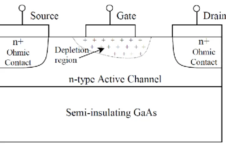
A MESFET is a three-terminal device like any other transistor [13]. These terminals are named as Source, Drain and Gate as shown in Figure I.1 Charge carriers (electrons) flow from the source to the drain via a channel. The channel is defined by doping the epitaxial layer grown on semiconductor and offers good conduction. The flow of charge carriers in the channel is controlled by a Schottky barrier gate. The main advantages of a MESFET compared to its counter parts are:
(a) high electron velocity inside the channel;
(b) smaller transit time leading to faster response and
(c) fabrication of active layer on semi-insulating GaAs substrates to decrease the parasitic capacitances [10].
Chapter I Study of the conventional structure of MESFET
5
3. GaAs MESFET
For microwave and millimeter wave frequencies, the MESFET devices are fabricated using GaAs material [11].
The substantial improvement in FET performance by using GaAs substrate over the Silicon is mainly attributed to the fact that:
a. The conduction band electrons in GaAs have approximately six times higher mobility and twice the peak drift velocity as that of Silicon. This leads to low parasitic resistances, large transconductance and shorter transit time.
b. The larger band gap in GaAs devices allows higher working temperature. This is particularly important in the small geometry of power devices which are used at microwave frequencies and dissipates a lot of heat. Furthermore, due to the relatively large band gap, GaAs devices operating at room temperature offer low thermal leakage current and thus provide a low noise figure[10].
A thin layer of n-type GaAs is deposited on top of a semi-insulating GaAs substrate. The back face of the substrate is covered with a metal Au/Ge alloy [14], which is usually connected to the source terminal during measurements. Both drain and source are connected to the n-type layer through n+ ohmic contacts. The metal of the source and drain electrodes can be made of Au/Ge alloy, which is coated with Ti, Pt, and Au layers, respectively. The gate is a thin layer of metal, usually aluminum coated with Au, deposited on top of the n-type layer between drain and source. The metal semiconductor junction of the gate represents a Schottky barrier junction. This junction is used to control the height of the active channel layer beneath the gate by applying a bias voltage to the gate. The area just beneath the gate is charge depleted as per the applied bias.
The most important dimensions of a MESFET device are the gate length “L” and width “W”. Those dimensions usually characterize the device. For example, a device can be referred as 0.3x300 μm2 when the gate length is equal to 0.3 µm and the gate width is equal to 300 µm. A typical value of gate length ranges from 0.1 to 1 µm. The gate length determines the maximum frequency of operation. As the gate length decreases, the maximum frequency increases . On the other hand, the gate width determines the performance of the device such as the maximum current capability [11].
Chapter I Study of the conventional structure of MESFET
6
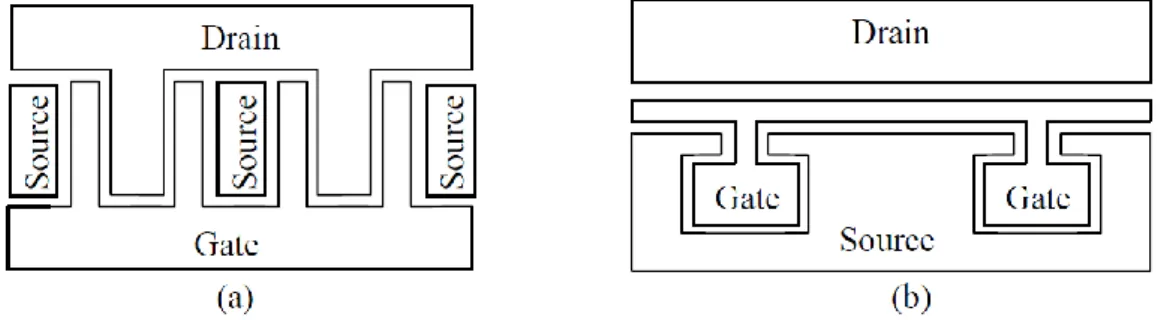
Figure I.2: Actual GaAs MESFET layouts: (a) interdigitated-gate, (b) π-gate.
The actual layout of a MESFET device is more complex than that shown in Figure I.1. Figure I.2 shows two different examples of actual layouts: interdigitated-gate and π-gate layout. Those layouts are usually used to increase the gate width while decreasing the parasitic gate resistance. The patterns shown in Figure I.2 can be repeated to achieve the required gate width. This layout implies crossover areas between metalization traces, which should be filled with either silicon dioxide or air [14].
4. MESFETs operation
The operation of a GaAs MESFET is similar to Si JFET, but the only difference is, in GaAs MESFET a metal semiconductor rectifying contact is used at the gate instead of a pn junction of a JFET [15].
A MESFET device is biased by applying two voltages: Vgs between gate and
source and Vds between drain and source. These voltages control the channel current
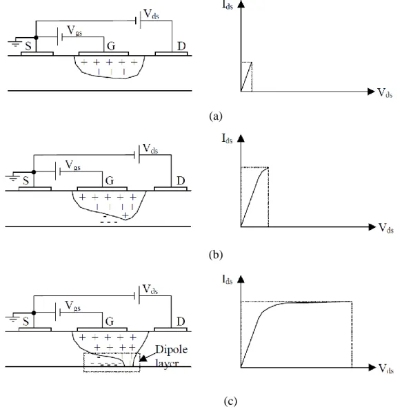
between the drain and source by varying the height of the gate-depletion region and the longitudinal electric field. The operation can be explained qualitatively without going into deep physical analysis. Three cases can be recognized for the Ids-Vds characteristic curve
of the MESFET, if Vgs is larger than the pinch-off voltage,: low Vds voltage where Ids is
linearly proportional to Vds, high Vds where the current is almost constant, and moderate
Vds where Ids has nonlinear relationship of Vds.
Imagine first that Vgs=0 and Vds is raised from zero to some low value as shown
in Figure I.3(a). When Vgs=0, the depletion region under the Schottky-barrier gate is
relatively narrow, and as Vds is raised, a longitudinal electric field and current are established in the channel. Because of Vds, the voltage across the depletion region is
Chapter I Study of the conventional structure of MESFET
7
greater at the drain end than at the source end, so the depletion region becomes wider at the drain end.
The narrowing of the channel and the increased Vds increase the electric field
near the drain, causing the electrons to move faster. Although the channel depth, and in turn channel’s conductive cross section, is reduced, the net effect is increased current. When Vds is low, the current is approximately proportional to Vds. However, if the gate
reverse bias is increased while the drain bias is held constant, the depletion region widens and the conductive channel becomes narrower, reducing the current. When Vgs=Vp, the
pinch-off voltage, the channel is fully depleted and the drain current is zero, regardless of the value of Vds. Thus, both Vgs and Vds can be used to control the drain current. When
the MESFET is operated under such bias voltages, where both Vgs and Vds have a strong
Chapter I Study of the conventional structure of MESFET
8
Figure I.3: GaAs MESFET operation under different Vds biasing with Vgs ≤ 0: (a)
Linear region (Vds is very low), (b) Vds at the onset of saturation, (c) Vds is
big.
If Vds is raised further, as shown in Figure I.3(b), while Vgs is larger than the
pinch-off voltage, the channel current increases, the depletion region becomes deeper at the drain end, and the conductive channel becomes narrower. The current clearly must be constant throughout the channel. As a result, and as long as the conductive channel near the drain becomes narrower, the electrons must move faster. However, the electron velocity cannot increase indefinitely; the average velocity of the electrons in GaAs cannot exceed a velocity called the saturated drift velocity.
If Vds is increased beyond the value that causes velocity saturation (usually only
a few tenths of a volt), the electron concentration rather than velocity must increase in order to maintain current continuity. Accordingly, a region of electron accumulation
(a)
(b)
Chapter I Study of the conventional structure of MESFET
9
forms near the end of the gate. Conversely, after the electrons transit the channel and move at saturated velocity into the wide area between the gate and drain, an electron depletion region is formed. The depletion region is positively charged because of the positive donor ions remaining in the crystal. As Vds is increased further, as shown in
Figure I.3(c), progressively more of the voltage increase is dropped across this region to enforce the electrons to cross it and less is dropped across the unsaturated part of the channel. This region is called a dipole layer or charge domain. Eventually, a point is reached where further increase in Vds is dropped entirely across the charge domain and
does not substantially increase the drain current. At this point, the electrons move at saturated drift velocity over a large part of the channel length. When the MESFET is operated in this manner, which is the normal mode of operation for small-signal devices, it is said to be in its saturated region.
Accurate models may include the effect of the charge domain in some way. Therefore, some models include a capacitor between the drain and the gate-source equivalent circuit to account for the charge domain [11].
5. MESFET characteristics 5.1 I-V characteristics
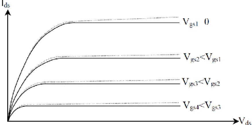
The I-V characteristic curves of a MESFET device are shown in Figure I.4 for an ideal and actual MESFET. The curves are plotted for different values of Vgs. It is
obvious that the actual I-V curve exhibits finite positive slope in the saturation region. Many reasons may be responsible for this phenomenon. One of the most dominant reasons in a short gate device is the carrier injection into the semi-insulating substrate. This finite slope is the source of the finite output conductance in a MESFET model [11].
Chapter I Study of the conventional structure of MESFET
10
Figure I.4: I-V Characteristic curves for a MESFET device for different values of Vgs;
ideal current is drawn in solid curve while dashed curve indicates the actual current.
5.2 Transconductance & output conductance
The
transconductance gm is a measure of the incremental change in the output current Ids for a given change in the internal input voltage Vgs. The internal input voltage is the voltage
across the gate source junction. In other words, the device transconductance is defined as the slope of the Ids-Vgs characteristics with the drain-source voltage held constant. The
mathematical statement of this definition can be expressed as: 𝑔𝑚 =𝜕𝐼𝑑𝑠
𝜕𝑉𝑔𝑠|𝑉
𝑑𝑠=𝑐𝑜𝑛𝑠𝑡𝑎𝑛𝑡
(I.1)
The transconductance of the device is one of the most important indicators of the device quality for microwave and millimeter wave applications. When all other characteristics are equal, a device with high transconductance will provide greater gains and superior high frequency performance. The transconductance suffers from what is called low frequency dispersion. The low frequency dispersion is the phenomenon of a parameter variation at low frequencies. The low frequency dispersion takes place as a result of the deep levels in the device structure. So, it significantly depends on the semiconductor material quality and fabrication processes [11].
The output resistance Rds is the incremental resistance between drain and source,
and it is more convenient to be explained in terms of its reciprocal, the output conductance gds.
Chapter I Study of the conventional structure of MESFET
11
The output conductance is a measure of the incremental change in output current Ids with the output voltage Vds. So, it can be defined as the slope of the Ids-Vds
characteristics with the gate-source voltage held constant. Mathematically, the output conductance and resistance can be defined by:
𝑔𝑑𝑠 = 1 𝑅𝑑𝑠 = 𝜕𝐼𝑑𝑠 𝜕𝑉𝑑𝑠|𝑉 𝑔𝑠=𝑐𝑜𝑛𝑠𝑡𝑎𝑛𝑡 (I.2) [11] The output conductance of the device is an important characteristic in analog applications. It plays a significant role in determining the maximum voltage gain attainable from the device and is extremely important for determining optimum output matching properties. In general, for a device to have a low value output conductance is desirable, or, equivalently, an extremely high output resistance.
For devices with equivalent gate widths, short gate lengths typically result in lower output resistances. The output resistance can also be reduced by increasing channel doping concentrations, Nd, or the device epi-thickness. The device transconductance is
defined as the slope of the Ids-Vgs characteristics with the drain-source voltage held
constant [16].
5.3 Cut off frequency
The cut-off frequency fT is defined as the frequency when the current gain is
unity, and is related to the transconductance gm.
𝑓𝑇 = 𝑔𝑚
2𝜋𝐶𝐺𝑆 (I.3)
Where CGS is the gate-source capacitance. As with other transit time devices, the
MESFET will operate up to a frequency which is related to the finite time it takes for a charge carrier to flow under the gate to the output. In order to see how this dictates the cut-off frequency fT, we assume the gate length is L and the electron travels at a speed v.
Let the time it takes to travel under the gate be τ. The phase change of the gate voltage has to be small in order for amplification to be useful, thus
2𝜋𝑓𝑇𝜏 =2𝜋𝑓𝑇𝐿
𝑣 < 1 (I.4)
Or
𝑓𝑇 < 𝑣
Chapter I Study of the conventional structure of MESFET
12
6. Conclusion
The GaAs material is prominent for optoelectronic applications and electronic devices. In addition, it has a potential for higher speed operation than silicon and Germanium in electronic applications. In this chapter, we have discussed about the GaAs MESFET, its operation and its different characteristics have been presented. Important parameters such as cut off frequency and transconductance, which are determined the figure of merit for analyzing the MESFET at high frequency are also illustrated.
Chapter II Study of DM GaAs MESFET-based design
13
Chapter II
Study of DM GaAs MESFET-based design
1. Introduction
In today’s world, high frequency communication and power applications are possible because of the superior electrical properties offered by III-V based MESFETs both in analog as well as in digital applications. Although III-V based MESFETs have good performances for high frequency and speed circuit applications, potential ways to enhance them for high frequency, high power and microwave applications is still worth investigating. Numerous III-V based MESFET structures have been reported and investigated to have reached this goal and optimized over the last few years [18-21].
In this chapter, we investigate the performance of the Dual-Material-gate (DM) GaAs MESFET-based design. This latter will be studied and analytical models are presented in order to improve the electrical behavior of the device for analog applications. Moreover, drain-current characteristics of both structures (single material and dual material) are compared in order to show the advantages provided by the DM GaAs-MESFET design.
Chapter II Study of DM GaAs MESFET-based design
14
2. Device structure and Models formulation
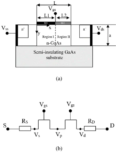
A schematic cross section of a DM GaAs-MESFET and the definition of the geometrical and electrical characteristics are shown in Figure II.1. As shown in the figure,
a is the GaAs film thickness, L is the channel length, L1 is the length of the first region
and ND/S represents the doping level of the drain/source region respectively. Using an
equivalent circuit analogy, a DM GaAs-MESFET device can be represented as a series combination of two GaAs-MESFETs with different material-gate work functions as shown in FigureII.1(b).
(a)
(b)
Figure II.1: (a) Cross-sectional view of the analyzed DM GaAs-MESFET (b) equivalent circuit representation for a drain current modeling.
In submicron GaAs-MESFETs, quite often, there is a finite density of interface states and the ideal device pinch-off is usually not observed [6]. The Schottky interfacial layer, which is a probable cause of the threshold voltage shift, is assumed to be of finite thickness that can hold potential across it and, on the other words, it is transparent enough to allow the flow of electrons [6]. Devices with interfacial layers exhibit relatively higher
Chapter II Study of DM GaAs MESFET-based design
15
gate leakage and consequently the effect of gate potential to control the channel thickness is poor. The loss of finite amount of gate voltage due to the interfacial layer has not been incorporated in most models presented in literature [6]. They assumed an ideal Schottky interface of a GaAs-MESFET and as a result these models are not accurate enough to simulate Current-Voltage characteristics of a device having finite Schottky barrier interfacial layer. In this study, a comprehensive drain current model is proposed which is an extension to N.M. Memon model capable to simulate drain current behavior of Single Material Gate (SM) GaAs-MESFETs irrespective of the Schottky barrier response [6].
Based on the drain current model proposed by Memon et al for a Single Material Gate (SM) GaAs-MESFET, the analytical expression of the drain current, including the interface states effects, can be given as
) V 1 )( V tanh( V V V V 1 I I ds ds 2 ds th th eff dss ds , (II.1)
where Idssis the saturation drain current, Vdsis the applied drain voltage, Vth
represents the threshold voltage,
Vthis the threshold voltage shift caused by the interfacestate effects, V represents the effective applied gate voltage given [6] by eff
bi gs V V bi gs eff e 1 V V V
, with Vbi represents the schottky-barrier built-in potential, which
mainly depends on material gate work function, and represents a constant which simulates quality of schottky barrier. In Eq. (II.1) there are four fitting parameters which describe the short-channel effects on the electrical characteristics [6].
In a SM GaAs MESFET, the gate consists of only one material, but in the proposed design (DM), we have two different materials with work functions
M1and
M2, respectively. Therefore, the schottky-barrier built-in potential Vbi at the gate, for eachregion, would be different. From the equivalent circuit in Figure II.1, Vds Vp Vdp is obtained. Therefore, the drain current for each transistor can be derived using Eq. II.1 and the boundary condition which satisfies the continuity of the channel potential and the drain current at the interface of two dissimilar gate-materials of the gate. Therefore, we have: 2 ds 1 ds ds I I I (II.2a)
Chapter II Study of DM GaAs MESFET-based design 16
)
V
1
)(
V
tanh(
V
V
V
V
1
I
)
V
(
I
p p 2 p 1 th 1 th 1 eff 1 dss p 1 ds
(II.2b)))
V
V
(
1
))(
V
V
(
tanh(
)
V
V
(
V
V
V
1
I
)
V
(
I
ds p ds p 2 p ds 2 th 2 th 2 eff 2 dss p 2 ds
(II.2c) where the threshold voltage and shift in threshold due to submicron geometry of the both devices are defined, respectively, as:For the first region:
1 bi 2 1 th 2 qNa V (II.3a) 1 1 1 3 4 th th V L a V (II.3b)
For the second region:
2 bi 2 2 th 2 qNa V (II.4a) 2 th 1 2 th V ) L L ( 3 a 4 V (II.4b)
Based on the boundary conditions and the drain current expression for each region (given in (II.2)), the interfacial potential (Vp) can be calculated numerically, and therefore,
a new drain current model which includes the dual-material gate aspect can be obtained [22].
The values of the small signal parameters (transconductance,gm, and out
conductance,gd ) are derived by differentiating Ids, given in Equation (II.2), with respect to V and gs Vds respectively.
Chapter II Study of DM GaAs MESFET-based design 17
p p
p 1 th 1 th V V 1 eff 1 bi gs 1 eff p 1 th 1 th 1 eff 1 dss m V 1 V tanh V V V 1 e V 1 V V V V V V V 1 I 2 g gs bi1 (II.5a)
p 2 p 1 th 1 th 1 eff 1 dss p p 2 2 p 1 th 1 th 1 eff 1 dss p p 2 p 1 th 1 th 1 eff p 1 th 1 th 1 eff 1 dss d V tanh V V V V 1 I V 1 V tanh 1 V V V V 1 I V 1 V tanh V V V V 1 V V V V 1 I 2 g (II.5b) In order to fully benefit from the expected performance of the coming technology nodes, all the parasitic components have to be reduced as much as possible. In particular, the parasitic device resistances, which are the drain resistance in series with the source one, will have to be drastically decreased as we will reduce the device length. In addition, the channel resistance can be considered as the most important parameter which affects the device power consumption. Hence, the minimisation of this parameter should be taken into account by the circuits designer [22].The equivalent MESFET resistance can be represented as a series combination of two parasitic resistances and output resistance as
1 d D s 1 d Par eq R g R R g R (II.6) With: n d gs S Wa qN L R , n d gd D Wa qN L R .
where Rsand
R
D represent the source and drain resistances, respectively, L and gs Ldsrepresent the gate-source and gate-drain lengths, respectively, and
nrepresents the low electron mobility for the GaAs material [23].Chapter II Study of DM GaAs MESFET-based design
18
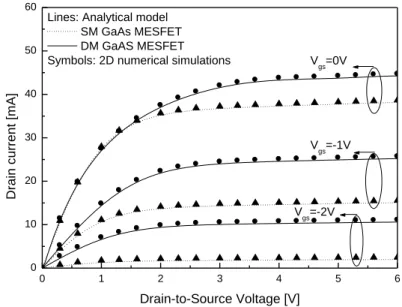
3. Results and discussion
In order to investigate the effectiveness of the proposed DM GaAs-MESFET design, the DM and SM structures are studied, compared and results are presented. Further the DM device results are compared with the simulated results of ATLAS 2D device simulator [24]. Figure II.2 shows the calculated output characteristics for a channel length of a 0.2200µm2 (
L
1
0
.
1
µm
) DM GaAs-MESFET compared with that of the conventional SM GaAs-MESFET. The device parameters for both designs, DM and SM, are: Nd 51017cm3; a 0.1µm; Vbi1 1.3V; Vbi2 0.21V . It is shown that the model calculations are in good agreement with the simulation results for a wide range of channel lengths. It can be observed that the DM GaAs-MESFET exhibits a better drain current behavior in the saturation regime. Due to the discontinuity in the channel potential of the DM GaAs-MESFET, the peak electric field at the drain is reduced substantially when compared with that of the SM GaAs-MESFET that leads to a reduced hot carrier and electron saturation velocity effects in the channel. These effects are considered as the main failure parameters which affect the device performances for analog circuits applications. The obtained results for both designs, SM and DM, show that the proposed structure offers significant improvement especially at low applied gate voltage. Therefore, as device dimensions penetrate into the submicron regime, the improved obtained performances make DM GaAs-MESFET a better choice for future submicron MESFET-based devices.Chapter II Study of DM GaAs MESFET-based design 19 0 1 2 3 4 5 6 0 10 20 30 40 50 60 Vgs=-2V Vgs=-1V Vgs=0V D ra in c u rr e n t [m A] Drain-to-Source Voltage [V] Lines: Analytical model
SM GaAs MESFET DM GaAS MESFET Symbols: 2D numerical simulations
Figure II.2: Output characteristics for a channel length of a 0 .2 200µm2(
L
1
0
.
1
µm
)DG MESFET compared with that of the conventional SM GaAs-MESFET. Device parameters used for calculating are
3 17 d 2 bi 1 bi 2 M 1 M 5.3eV, 4.28eV,V 1.3V,V 0.21V N 5.10 cm , µm 1 . 0 a .
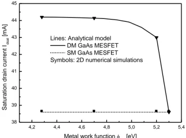
Figure II.3 plots the variation of the saturation drain current,Idsat,DM, as function of metal gate work function near the drain end,
M2, for a fixedµm L and eV V V V
Vgs 0 , ds 6 , M1 5.3 10.1 . It is clear shown that as gate metal work function near the drain end increases, Isat,DM, decreases; this is due to the increase
in the threshold voltage. This also implies that higher value of
M2 results in higher threshold voltage that is unsuitable and poses a trade off with power supply requirements [22].Chapter II Study of DM GaAs MESFET-based design 20 4,2 4,4 4,6 4,8 5,0 5,2 5,4 38 39 40 41 42 43 44 45 S aturation dra in curre nt Idsa t [ mA ]
Metal work function M2 [eV] Lines: Analytical model
DM GaAs MESFET SM GaAs MESFET
Symbols: 2D numerical simulations
Figure II.3: variation of the saturation drain current,Idsat, as function of metal gate
work function near the drain end,
M2, for a fixedµm L and eV V V V Vgs 0 , ds 6 , M1 5.3 1 0.1 .
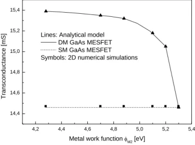
Figure II.4(a) shows the variation of the transconductance as a function of increasing work function of the metal gate near the drain end at fixed ,
M2, for a fixedµm 1 . 0 L and eV 3 . 5 , V 4 V , V 0
Vgs ds M1 1 . It is shown that as the
M2 is increasedthe gm keeps on decreasing due to a reduced gate overdrive. This effect can be explained
by the effect of the increasing in the work function of the metal near the drain on the increasing of the threshold voltage. Figure II.4(b) plots the variation of output conductance, gd, with the increase in the work function of the gate metal near the drain end. It is clear shown that gdis increased with the increase in
M2. This is due to the factthat with the increase in
M2, the region near the drain is screened from any variations in the drain bias. This reduces the influence of drain bias on the drain current in the saturation regime [22].Chapter II Study of DM GaAs MESFET-based design 21 4,2 4,4 4,6 4,8 5,0 5,2 5,4 14,4 14,6 14,8 15,0 15,2 15,4 Transcon ductance [mS ]
Metal work function M2 [eV] Lines: Analytical model
DM GaAs MESFET SM GaAs MESFET
Symbols: 2D numerical simulations
(a) 4,2 4,4 4,6 4,8 5,0 5,2 5,4 500 550 600 650 700 750 800 850 900 Ou tp u t co n d u c ta n c e [µS]
Metal work function M2 [eV] Lines: Analytical model
DM GaAs MESFET SM GaAs MESFET
Symbols: 2D numerical simulations
(b)
Figure II.4: (a) Variation of the transconductance as a function of increasing work function of the metal gate work function for a fixed
µm L and eV V V V Vgs 0.5 , ds 4 ,M15.3 1 0.1 . (b) Variation of the
output conductance with the increase in the work function of the gate metal near the drain end.
Chapter II Study of DM GaAs MESFET-based design
22
4. Conclusion
In this work, the concept of Dual-Material Gate has been applied to the GaAs-MESFET structure and the features exhibited by the resulting new device have been investigated and analyzed by developing new analytical models, which describe the device behavior for analog applications. It has been demonstrated that Dual-Material Gate design offers superior characteristics in terms of drain current and transconductance enhancement and reduced output conductance. Moreover, the improvement of these parameters will also enhance the device performance for high frequency and high power applications.
Chapter III Modeling of TM GaAs MESFET-based design
23
Chapter III
Modeling of TM GaAs MESFET-based
design
1. Introduction
III–V based metal semiconductor field effect transistors (MESFETs) have received a great deal of attention both in high frequency and high power applications [20]. GaAs MESFETs technology is used due to its superior characteristics such as large bandgap, high breakdown voltage, large saturation velocity and high thermal conductivity, which makes it suitable for high frequency, high temperature, and high power applications [3-6].
In this chapter, we have developed a new analytical compact model for I –V characteristics with the effect of gate-engineering in order to suppress the short channel effects for deep submicron GaAs MESFET-based circuits. The model is further extended to evaluate the transconductance and cut-off frequency including the effect of third region length. The results so obtained are verified using the ATLAS 2D device simulation software [24].
Chapter III Modeling of TM GaAs MESFET-based design
24
2. Device structure and Models formulation
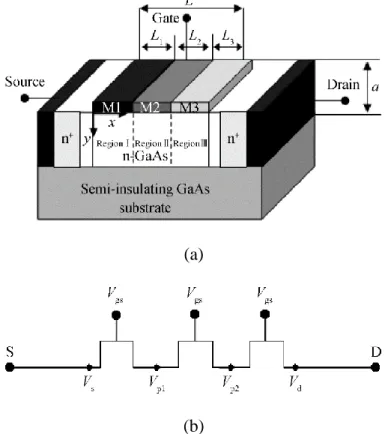
A schematic cross-sectional view of the proposed TM GaAs-MESFET is presented in Figure III.1(a). As shown in Figure III.1, the gate consists of three materials M1, M2 and M3. L1, L2 and L3 represent the lengths of the first, second and third regions of the channel layer with work functions ØM1, ØM2 and ØM3, respectively. The work
functions are chosen in such a way that ØM1 > ØM2 > ØM3 and L = L1 + L2 + L3 [8]. The
gate material of the first region (near the source end) is with the highest work function called the control gate, the material of the second region is with the intermediate work function called the first screen gate and the material of the third region (near the drain end) is with the lowest work function called the second screen gate[25]. ND/S represents
the doping level of the drain/source region, respectively. The channel region is bounded by source and drain spacing at x = 0 and L, respectively, where L is the gate length and a is the thickness of the active layer. At y = 0 and y = a, it is bounded by the interface of gate metal and the n-GaAs active region and the bulk, respectively.
The equivalent circuit of the TM GaAs-MESFET design can be represented as a series combination of three GaAs MESFETs with different material-gate work functions as shown in Figure III.1(b).
Chapter III Modeling of TM GaAs MESFET-based design
25 (a)
(b)
Figure III.1: (a) Cross-sectional view of the analyzed TM GaAs MESFET. (b) Equivalent circuit representation for a drain current modeling.
To simulate the output characteristics of submicron GaAs MESFETs having a finite interfacial layer, where the latter is assumed to be of finite thickness that can hold potential across it and, in other words, it is transparent enough to allow the flow of electrons [6], a complete analytical drain current model is proposed which is an extension of the Memon and Djeffal models. These models are used to investigate and to study the drain current behavior of both single material gate (SM) and dual material gate (DM) GaAs-MESFETs. The modeling of the gate-engineering device characteristics is based on models proposed by Memon et al.[6] and Djeffal et al.[7] for single and dual material gate GaAs MESFETs. The analytical model of the drain current for SM can be given as 𝐼𝑑𝑠 = 𝐼𝑑𝑠𝑠(1 − 𝑉𝑒𝑓𝑓
𝑉𝑡ℎ+∆𝑉𝑡ℎ+𝛾𝑉𝑑𝑠)
2tanh (𝛼𝑉
𝑑𝑠)(1 + 𝜆𝑉𝑑𝑠), (III.1)
where Idss is the saturation drain current, Vds is the applied drain voltage, Vth represents
the threshold voltage, ΔVth is the threshold voltage shift caused by the interface state
effects, and Veff represents the effective applied gate voltage given [6] as a function of the
Chapter III Modeling of TM GaAs MESFET-based design
26 𝑉𝑒𝑓𝑓 = 𝑉𝑔𝑠− 𝑉𝑏𝑖
1 + 𝜂𝑒𝑉𝑔𝑠−𝑉𝑏𝑖
The latter is mainly dependent on material gate work function. There are four fitting parameters in Equation (III.1) which describe the short-channel effects on the electrical characteristics [6, 7]. These parameters are α; λ; γ and η.
In SM and DM structures, the gate consists of only one material (for the first case) or two materials (for the second structure), whereas in the proposed design (TM), the gate consists of three different materials with different work functions ØM1, ØM2 and
ØM3, respectively. So, the Schottky-barrier built in potential at the gate, for each region,
would be different. According to the equivalent circuit presented in Figure 1(b), the electric field and potential in the channel is continuous at the junction between the gate materials M1 and M2 as well as between M2 and M3. Therefore, the drain current model for each transistor incorporating the gate material aspect can be derived using Equation (III.1) and it can be written as
𝐼𝑑𝑠 = 𝐼𝑑𝑠1 = 𝐼𝑑𝑠2= 𝐼𝑑𝑠3, (III.2) 𝐼𝑑𝑠1(𝑉𝑝1) = 𝐼𝑑𝑠𝑠1(1 − 𝑉𝑒𝑓𝑓1 𝑉𝑡ℎ1+∆𝑉𝑡ℎ1+𝛾𝑉𝑝1) 2tanh (𝛼𝑉 𝑝1)(1 + 𝜆𝑉𝑝1), (III.3) 𝐼𝑑𝑠2(𝑉𝑝1, 𝑉𝑝2) = 𝐼𝑑𝑠𝑠2(1 − 𝑉𝑒𝑓𝑓2 𝑉𝑡ℎ2+ ∆𝑉𝑡ℎ2+ 𝛾(𝑉𝑝2− 𝑉𝑝1)) 2 × tanh (𝛼(𝑉𝑝2− 𝑉𝑝1))(1 + 𝜆(𝑉𝑝2− 𝑉𝑝1)), (III.4) 𝐼𝑑𝑠3( 𝑉𝑝2) = 𝐼𝑑𝑠𝑠3(1 − 𝑉𝑒𝑓𝑓3 𝑉𝑡ℎ3+ ∆𝑉𝑡ℎ3+ 𝛾(𝑉𝑑𝑠− 𝑉𝑝2)) 2 × tanh (𝛼(𝑉𝑑𝑠− 𝑉𝑝2))(1 + 𝜆(𝑉𝑑𝑠− 𝑉𝑝2)), (III.5) Where the threshold voltage and shift in threshold due to the submicron effect of the three transistors are given for each region, respectively, as
𝑉𝑡ℎ1= 𝑞𝑁𝑎2 2𝜀 − 𝜙𝑏𝑖1, (III.6) ΔV𝑡ℎ1= 4𝑎 3𝐿1𝑉𝑡ℎ1, (III.7) 𝑉𝑡ℎ2= 𝑞𝑁𝑎2 2𝜀 − 𝜙𝑏𝑖2, (III.8) ΔV𝑡ℎ2= 4𝑎 3𝐿2𝑉𝑡ℎ2, (III.9)
Chapter III Modeling of TM GaAs MESFET-based design 27 𝑉𝑡ℎ3= 𝑞𝑁𝑎2 2𝜀 − 𝜙𝑏𝑖3, (III.10) ΔV𝑡ℎ3= 4𝑎 3(𝐿−𝐿1−𝐿2)𝑉𝑡ℎ3, (III.11)
In order to find the drain current model of GaAs MESFET incorporating the gate-engineering aspect, the interfacial potentials (Vp1 and Vp2) can be calculated
numerically using the boundary conditions and the obtained drain current expressions for each region, and thus it can be developed.
The values of the small signal parameters can be derived by differentiating Ids in
function of Vgs and Vds to calculate the transconductance, gm and the output conductance,
gd. 𝑔𝑚 = 2𝐼𝑑𝑠𝑠1[1 − 𝑉𝑒𝑓𝑓1 𝑉𝑡ℎ1+ ∆𝑉𝑡ℎ1+ 𝛾𝑉𝑝1] × [ 𝑉𝑒𝑓𝑓1 𝑉𝑔𝑠− 𝑉𝑏𝑖1(1 − 𝜂𝑉𝑒𝑓𝑓1𝑒 𝑉𝑔𝑠−𝑉𝑏𝑖1)] × [ −1 𝑉𝑡ℎ1+Δ𝑉𝑡ℎ1+𝛾𝑉𝑝1] × [tanh(𝛼𝑉𝑝1) (1 + 𝜆𝑉𝑝1)], (III.12) 𝑔𝑑 = 2𝐼𝑑𝑠𝑠1[1 − 𝑉𝑒𝑓𝑓1 𝑉𝑡ℎ1+ ∆𝑉𝑡ℎ1+ 𝛾𝑉𝑝1] × [1 − 𝛾𝑉𝑒𝑓𝑓1 (𝑉𝑡ℎ1+ ∆𝑉𝑡ℎ1+ 𝛾𝑉𝑝1)2] × 𝑡𝑎𝑛ℎ(𝛼𝑉𝑝1) (1 + 𝜆𝑉𝑝1) + 𝐼𝑑𝑠𝑠1[1 − 𝑉𝑒𝑓𝑓1 𝑉𝑡ℎ1+ ∆𝑉𝑡ℎ1+ 𝛾𝑉𝑝1] 2 × [1 − 𝑡𝑎𝑛ℎ2(𝛼𝑉 𝑝1)] (1 + 𝜆𝑉𝑝1) + 𝜆𝐼𝑑𝑠𝑠1[1 − 𝑉𝑒𝑓𝑓1 𝑉𝑡ℎ1+ ∆𝑉𝑡ℎ1+ 𝛾𝑉𝑝1] 2 × 𝑡𝑎𝑛ℎ(𝛼𝑉𝑝1), (III.13)
Cut off frequency is a figure of merit for analyzing TM GaAs MESFET performance at microwave frequency, it is important to understand the cut off frequency. It is given by
𝑓𝑡 = 𝑔𝑚
2𝜋(𝐶𝑔𝑠+𝐶𝑔𝑑) (III.14)
Cgs and Cgd are the gate–source and gate–drain capacitance, respectively,
𝐶𝑔𝑠= 𝜀𝑠𝐿𝑊(𝑎 − 𝐼𝑑𝑠
𝑞𝑁𝑑𝑣𝑠𝑎𝑡𝑊)
−1, (III.15)
𝐶𝑔𝑑= 𝜀𝑠𝜋ℎ𝑠𝑊
Chapter III Modeling of TM GaAs MESFET-based design
28
hs and hd are the depletion widths at the source and drain ends, respectively [26].
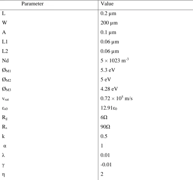
Table 1. Parameters used for the calculation of results shown in Figures III.(2-5). Parameter Value L W A L1 L2 Nd ØM1 ØM2 ØM3 vsat εs0 Rg Rs k α λ γ η 0.2 µm 200 µm 0.1 µm 0.06 µm 0.06 µm 5 × 10²³ m-3 5.3 eV 5 eV 4.28 eV 0.72 × 10⁵ m/s 12.91ε0 6Ω 90Ω 0.5 1 0.01 -0.01 2
Chapter III Modeling of TM GaAs MESFET-based design
29
3. Results and discussion
In this work, the calculated results for different structures TM, DM and SM are compared and verified using simulation results from ATLAS. The parameter values used for calculation are given in Table 1.
Figure III.2 shows the comparisons of output characteristics for the channel length of 0.2 × 200 µm2 TM, DM and SM GaAs MESFET structures. Good agreement between the model results and numerical simulation ones is obtained. It is noticed that the TM GaAs-MESFET demonstrates a better drain current behavior. It is evident that as compared to a single step change in channel potential in the DM design, there are two step changes in channel potential profile of the TM structure. This additional step change for TM GaAs-MESFETs can effectively reduce the peak electric field near the drain side compared with that of the DM and SM GaAs MESFETs that leads to a reduced electron saturation velocity effect in the channel, and therefore, the electron effective mobility in the channel will be increased. The obtained results for the different designs show that the TM structure exhibits significant improvement, particularly at a low applied gate voltage. Therefore, as the device dimensions penetrate into the submicron regime, the improved obtained performance makes TM GaAs-MESFET a better choice for MESFET-based devices [27].
Figure III.3 plots the variation of drain current against the drain voltage of TM GaAs-MESFET with different lengths of third region at Vgs=-1V. It is observed from the
figure that as the length of third region L3 (keeping the same channel length of the device i.e 0.2µm) decreases, the drain current degrades. This is due to the position of the second step change in channel potential profile of TM design which is closer to the drain side. However, as L3 increases, the drain current increases. In this case, the position of the second step change in channel potential profile is a little far from the drain side compared with that of the first case, the peak electric field is significantly reduced, therefore, the hot carrier effect is reduced and also electron mobility will be increased. Hence, the electrical behavior of the TM design can be enhanced by increasing the third region length.
Chapter III Modeling of TM GaAs MESFET-based design
30
Figure III.2: Output characteristics for a channel length of 0.2 × 200 µm2 TM GaAs
MESFET compared with that of the SM and DM GaAs MESFETs.
Figure III.3: Output characteristics for a channel length of 0.2 × 200 µm2 TM GaAs
MESFET with deferent length of the third region for a fixed Vgs=-1V
Chapter III Modeling of TM GaAs MESFET-based design
31
In the figure III.4 the transconductance is calculated as a function of gate voltage with different lengths of third region. It is clearly seen that the transconductance is affected when L3 decreases. This is due to reduction of drain current with decreasing of L3. Therefore, This reduction in current can be explained by the degradation of the mobility which is affected by the elevated electric field when L3 decreases. The microwave performance degradation is evidently observed (shown in figure III.5) when minimizing L3. This is due to the influence of third region on transconductance, which affect the cut off frequency. Moreover, the modification of the third region length of TM design can significantly vary the cut off frequency. Thus, it is necessary to choose the optimal third region length for microwave frequency applications.
Figure III.4: Variation of Transconductance with gate to source voltage for a channel
length of 0.2 × 200 µm2 TM GaAs MESFET with deferent length of the third
Chapter III Modeling of TM GaAs MESFET-based design
32
Figure III.5: Variation of cut-off frequency with drain to source voltage for a channel
length of 0.2 × 200 µm2 TM GaAs MESFET with deferent length of the third
Chapter III Modeling of TM GaAs MESFET-based design
33
4. Conclusion
In this work, an approach of a Triple Material Gate (TM) GaAs MESFET has been proposed, modeled and analyzed to suppress the short channel effects and improve the electrical behavior of the device. It has been found that the device performance can be greatly improved by incorporating the gate- engineering aspect. The influence of the length of third region on various parameters like I-V characteristic, transconductance and cut off frequency has been illustrated. It is clearly shown that a significant improvement in electrical performance is evidenced in TM design compared to DM and SM designs. Therefore, a noticeable enhancement in microwave performance is showed as a length of third region increased. Thus, in the submicron domain, the TM GaAs MESFET provides substantial enhancement in the performance which makes it suitable for microwave frequency applications.
34
Conclusion
Modern technology depends almost entirely on the transistor. ICs manufacturing use III-V based FET in forms of MOSFETs or MESFETs, due to their proprieties. GaAs in MESFET’s fabrication grants large transconductance, shorter transit time and large band gap compared to silicon. However, the usage of MESFET devices in wireless communications and microprocessors encountered many problems with scaling low power.
Today’s, researches try to immunize the GaAs MESFET against the short channel effects in order to enhance the scaling capability and the device performance for microwave frequency applications.
In this memory, the conventional GaAs MESFET has been described, we also talked about its operation, different characteristics and parameters such as cut off frequency and transconductance. The concept of Dual-Material Gate has been applied to the GaAs-MESFET structure and it has been analyzed by developing new analytical models. The found results demonstrates that Dual-Material Gate design offers superior characteristics in terms of drain current and transconductance enhancement and reduced output conductance. Moreover, the improvement of these parameters will also enhance the device performance for high frequency and high power applications. With a view to further improving the previous characteristics a Triple Material Gate (TM) GaAs MESFET has been proposed, modeled and analyzed. The obtained results show that the additional material gate improves the device performance. The influence of the length of third region on various parameters like I-V characteristic, transconductance and cut off frequency has been illustrated. It is clearly shown that a significant improvement in electrical performance is evidenced in TM design compared to DM and SM designs. Therefore, a noticeable enhancement in microwave performance is showed as a length of third region increased. The obtained results make the proposed design suitable for microwave frequency applications.
Bibliography
[1] S. Oktyabrsky and D. Y. Peide, Fundamentals of III-V semiconductor MOSFETs. Springer, 2010.
[2] M. S. Shur, GaAs devices and circuits. Springer Science & Business Media, 2013. [3] M. M. Ahmed, "An improved method to estimate intrinsic small signal parameters of a GaAs MESFET from measured DC characteristics," IEEE Transactions on
Electron Devices, vol. 50, no. 11, pp. 2196-2201, 2003.
[4] M. Islam and M. Zaman, "A seven-parameter nonlinear I–V characteristics model for sub-μm range GaAs MESFETs," Solid-State Electronics, vol. 48, no. 7, pp. 1111-1117, 2004.
[5] U. Iqbal, M. Ahmed, and N. Memon, "An efficient small signal parameters estimation technique for submicron GaAs MESFET's," in Emerging
Technologies, Proceedings of the IEEE Symposium on, 2005.
[6] N. Memon, M. Ahmed, and F. Rehman, "A comprehensive four parameters I–V model for GaAs MESFET output characteristics," Solid-State Electronics, vol. 51, no. 3, pp. 511-516, 2007.
[7] F. Djeffal and N. Lakhdar, "An improved analog electrical performance of submicron Dual-Material gate (DM) GaAs-MESFETs using multi-objective computation," Journal of Computational Electronics, vol. 12, no. 1, pp. 29-35, 2013.
[8] N. Lakhdar and F. Djeffal, "New optimized dual-material (DM) gate design to improve the submicron GaN-MESFETs reliability in subthreshold regime,"
Microelectronics Reliability, vol. 52, no. 6, pp. 958-963, 2012.
[9] W. Brattain, "entry of December 1947, Laboratory Notebook, case 38139-7," Bell
Laboratories Archives.
[10] N. M. Memon, "Modeling techniques of submicron GaAs MESFETs and HEMTs," MUHAMMAD ALI JINNAH UNIVERSITY, 2008.
[11] Y. A. Khalaf, "Systematic optimization technique for MESFET modeling," Ph.D. dissertation, Polytechnic Institute, Virginia university, Virginia, 2000.
[12] J.-P. Colinge and C. A. Colinge, Physics of semiconductor devices. Springer Science & Business Media, 2005.
[13] R. Soares, GaAs MESFET circuit design (Artech House materials science library). Boston,Mass.: Artech, 1988.
[14] J. V. DiLorenzo and D. D. Khandelwal, "GaAs FET principles and technology,"
Dedham, MA, Artech House, Inc., 1982. 787 p, 1982.
[15] M. Shur, "Low field mobility, effective saturation velocity and performance of submicron GaAs MESFETs," Electronics Letters, vol. 18, no. 21, pp. 909-910, 1982.
[16] B. Kaur, "Physics based analytical Modeling of Gallium Arsenide MESFET for Evaluation Of Junction Capacitance with new modeling conception," Masters of Science thesis, Electrical Engineering, California State University Northridge, 2012.
[17] Z. Awang, Microwave Systems Design. Springer Science & Business Media, 2013.
[18] C. Lee, W. Lu, E. Piner, and I. Adesida, "DC and microwave performance of recessed-gate GaN MESFETs using ICP-RIE," Solid-State Electronics, vol. 46, no. 5, pp. 743-746, 2002.
[19] F. Djeffal, N. Lakhdar, M. Meguellati, and A. Benhaya, "Particle swarm optimization versus genetic algorithms to study the electron mobility in wurtzite GaN-based devices," Solid-State Electronics, vol. 53, no. 9, pp. 988-992, 2009. [20] N. Lakhdar, F. Djeffal, Z. Dibi, G. Ferro, and P. Siffert, "A Two‐Dimensional
Numerical Analysis of Subthreshold Performances for Double‐Gate GaN‐ MESFETs," in AIP Conference Proceedings, 2010.
[21] S. Kabra, H. Kaur, S. Haldar, M. Gupta, and R. Gupta, "Two-dimensional subthreshold analysis of sub-micron GaN MESFET," Microelectronics journal, vol. 38, no. 4, pp. 547-555, 2007.
[22] N. LAKHDAR, "Contribution to the modeling of III-V materials-based multi-gate transistors," Ph.D. dissertation, Department of Electronics, Université de Batna 2, Batna, 2012.
[23] K. Nummila, A. Ketterson, and I. Adesida, "Delay time analysis for short gate-length GaAs MESFETs," Solid-state electronics, vol. 38, no. 2, pp. 517-524, 1995.
[24] Software SILVACO International, "ATLAS: 2D Device Simulator," ed, 2008. [25] P. S. Dhanaselvam, N. Balamurugan, and V. Ramakrishnan, "A 2D
Transconductance and Sub-threshold behavior model for triple material surrounding gate (TMSG) MOSFETs," Microelectronics Journal, vol. 44, no. 12, pp. 1159-1164, 2013.