UNIVERSITÉ DE MONTRÉAL
DIFFERENTIAL INTEGRATOR PIXEL ARCHITECTURE FOR DARK
CURRENT COMPENSATION IN CMOS IMAGE SENSORS
MARZIEH MEHRI DEHNAVI
DÉPARTEMENT DE GÉNIE ÉLECTRIQUE,
ÉCOLE POLYTECHNIQUE DE MONTRÉAL
MÉMOIRE PRÉSENTÉ EN VUE DE L’OBTENTION
DU DIPLÔME DE MAÎTRISE ÈS SCIENCES APPLIQUÉES
(GÉNIE ÉLECTRIQUE)
AOÛT 2015
UNIVERSITÉ DE MONTRÉAL
ÉCOLE POLYTECHNIQUE DE MONTRÉAL
Ce mémoire intitulé :
DIIFFERENTIAL INTEGRATOR PIXEL ARCHITECTURE FOR DARK
CURRENT COMPENSATION IN CMOS IMAGE SENSORS
présenté par : MEHRI DEHNAVI Marzieh
en vue de l’obtention du diplôme de : Maîtrise ès sciences appliquées a été dûment accepté par le jury d'examen constitué de :
M. SAWAN Mohamad, Ph. D., président
M. AUDET Yves, Ph. D., membre et directeur de recherche
M. GAGNON Ghyslain, Ph. D., membre et codirecteur de recherche
DEDICATION
ACKNOWLEDGMENTS
I am deeply thankful to my supervisor, Dr. Yves Audet, for his guidance and encouragement throughout my Master studies at Ecole Polytechnique de Montreal. He has been an excellent advisor and a constant source of knowledge, motivation, and encouragement during this dissertation work. I would like to extend my thanks to Dr. Ghyslain Gagnon, my co-supervisor, for his guidance throughout this research work. I would like to thank the members of my committee, Dr. Mohamad Sawan and Dr. Abdelaziz Trabelsi for taking time to review my work.
Also I would like to thank to my colleagues at Microelectronics Research Group who were always there for me with countless help and constructive discussions.
I am continuously grateful to my family specially my parents for their support, love and encouragement.
Finally, I would like to thank all the staff members of the Electrical Engineering department at Ecole Polytechnique de Montreal for their direct and indirect help during my Masters study.
R
ÉSUM
ÉLe Capteur d'Image CMOS (CIS) est rapidement devenu la technologie dominante dans les marchés de l'imagerie. Il y a des avantages sur les technologies avec CCD tels que la faible consommation de puissance et les faibles coûts. . La technologie CMOS APS s’est améliorée au cours des dernières décennies et propose une alternative viable à la technologie CCD pour de nombreuses applications. Néanmoins, les capteurs d’image CMOS APS ont un niveau plus élevé de courant d'obscurité que les capteurs CCD. Plusieurs techniques ont été développées pour améliorer la performance du capteur d'image en termes de courant d'obscurité qui limite sévèrement la gamme dynamique et la sensibilité des capteurs d'image.
Il existe différentes approches pour réduire le courant d'obscurité. L'approche idéale, mais coûteuse, consiste à modifier le procédé de fabrication par améliorant la photosensibilité du pixel ou de réduire le courant de fuite. Cependant, certaines architectures de circuits peuvent être utilisées pour réduire ou compenser le courant d'obscurité sans modification de procédé, cette alternative fait l’objet de ce mémoire.
Dans cette thèse, un circuit amplificateur différentiel multi-branche est proposé pour compenser l'effet de courant d'obscurité d’un capteurs d'image CMOS. Afin d'obtenir une application de détection à faible courant de noirceur, un interrupteur de type T avec un faible courant de fuite est utilisé. La nouvelle configuration de multiple-input multiple-output amplificateur différentiel présente l'avantage de réduire considérablement les courants d'obscurité femto-ampères des photodiodes. L'objectif étant d’améliorer la sensibilité et la gamme dynamique des pixels des capteurs d'image CMOS. Un prototype est conçu à partir du procédé de fabrication CMOS standard 0.18 µm de TSMC.
ABSTRACT
CMOS Image Sensor (CIS) rapidly became the dominant technology over Charge-Coupled-Device (CCD) in imaging markets. It has many advantages over CCDs such as low power and low cost which is highly desirable for imaging-enabled mobile devices. CMOS Active Pixel Sensor (APS) technology has improved during the last decades and suggests a viable alternative for many applications with CCD technology. Nonetheless, CMOS APS image sensors have higher dark current level than CCD sensors. Several techniques have been developed to improve the performance of image sensor in terms of dark current which severely limits the dynamic range and the sensitivity of image sensors.
There are different approaches to reduce the dark current. The ideal but expensive approach is to modify the fabrication process by enhancing the photosensivity of the pixel or reducing the leakage current. However, some circuit and layout techniques reduce or compensate the dark current of standard CMOS processes which is the method considered in this work.
In this thesis a multi-branch differential amplifier circuit is proposed to compensate the effect of dark current in CMOS image sensors. In order to obtain a low level sensing application, a T-type switch with low leakage current is used. The new configuration of input multiple-output differential amplifier has the advantage of compensating the femto-ampere dark currents of photodiodes. The objective is to improve the sensitivity and the dynamic range of active pixel CMOS image sensors. A prototype is designed and simulated in a standard CMOS 0.18 µm fabrication process from TSMC.
TABLE OF CONTENTS DEDICATION……….. III ACKNOWLEDGMENTS……….IV RESUME………V ABSTRACT………..VI TABLE OF CONTENTS……….VII LIST OF TABLES…….………..X LIST OF FIGURES…….……….XI ABREVIATION……….…...XIV LIST OF APPENDICES……….XVII INTRODUCTION……….……….…...1 Motivation……….……….…...2 Objective……….…...2 Thesis organization……….…..2
CHAPTER 1 IMAGE SENSOR CHARACTERISTICS AND DARK CURRENT…….…..3
1.1 Image Sensor……….……...3
1.2 CMOS Image Sensor………...…3
1.2.1 Passive Pixel Sensor (PPS)……….…..4
1.2.2 Active Pixel Sensor (APS)……….…..4
1.2.3 Pinned Photodiode (PPD)……….…..5
1.2.4 Digital Pixel Sensor (DPS)……….…...7
1.3 Image Sensor Characteristics……….…..8
1.3.1 Fill Factor….……….………...8
1.3.2 Quantum Efficiency………....8
1.3.3 Dynamic range…….……….……….…..9
1.4 Dark Current………..10
1.4.2 Dark Current in P-N Photodiode……….……...10
1.4.3 Dark Current Reduction in Image Sensors……….………...13
1.5 Noise Associate with Dark Current in CMSO Image Sensors ….………..14
1.5.1 Fixed Pattern Noise……….………...15
1.5.2 Dark Current Shot Noise……….………..15
1.5.3 1/f Noise……….………...15
1.5.4 Reset Noise……….………...15
1.6 Leakage Current in MOSFET……….……….16
1.6.1 Reversed-biased Junction Leakage Current (IREV).……….17
1.6.2 Gate Induced Drain Leakage (GIDL)………...……….17
1.6.3 Gate Direct Tunneling………...……….18
1.6.4 Subthreshold Leakage.……….……….………18
1.7 Summar y……….…..19
2 CHAPTER 2 DESIGN OF IMAGE SENSOR PROTOTYPE………...…..20
2.1 MOSFET Switches……….…..20
2.1.1 Sample and Hold Circuit...………....……….20
2.2 Proposed Circuit Reducing the Effect of Dark Current in CMOS Image Sensor….…..28
2.2.1 Capacitance Transimpendance Amplifier (CTIA)..……….……...28
2.2.2 Leakage Current Reduction of Reset Switch..……….……...34
2.3 Actual Implementation……….….…..36
2.4 Subtractor Circuit………....39
2.5 Summary………..………....41
3 CHAPTER 3 POST-LAYOUT SIMULATION AND RESULTS……...………42
3.1 Simulation Results………....42
3.1.1 Simulation Result with Three Pixels...……….……...42
3.1.2 Subtractor Circuit...……….……….……...43
3.2 Comparing the Results of Different Switches...……….45
3.3 Dynamic Range………....46
3.4 Layout Design………....50
3.4.1 Capacitor..……..……….……….……...50
3.4.3 Photodiode..………...…..………….……….……...53
3.5 Pixel Layout………...54
3.6 Shift Register………...55
3.7 Circuit Simulation with Ten Pixels Including the Shift Register……….56
3.8 Analyzing of Parasitic Effect..………...58
3.9 Measuring the T-Switch Leakage..………...58
3.10 Monte Carlo Simulation………...………....60
3.10.1 Process Analyzis………..60
3.10.2 Analyzing the Effect of Process Variations in the Designed Structure………...61
3.10.3 Temprature Operating………..68
3.11 Summary………...………....70
CONCLUSION AND FUTURE WORK....………....71
REFERENCE………...……….……..73
LIST OF TABLES
Table 2. 1 Parameter values of the circuit of Figure 2.24……….39
Table 2. 2 Parameter values of subtractor circuit……….……….41
Table 3. 1 TSMC 0.18μm CMOS model parameters of photodiode……….53
Table 3. 2 Characteristics of the pixel………...54
Table 3. 3 Parameters of circuit in Figure 3.10……….57
Table 3. 4 MOSFET parameters and their relevant process steps………61
Table 3. 5 β, Vth of MOSFETs and slope value of a pixel output with IPD=30fA for 10 iterations ………..……….…67
LIST OF FIGURES
Figure 1. 1.a Pixel structure of PPS.………....4
Figure 1. 1.b structure of CMOS PPS………..4
Figure 1. 2.a Pixel structure of APS………....5
Figure 1. 2.b Structure of CMOS APS………....5
Figure 1. 3 Pixel structure of Pinned Photodiode APS………...6
Figure 1. 4 Readout timing diagram of a PPD APS………...7
Figure 1. 5.a Pixel structure of DPS………....7
Figure 1. 5.b Structure of CMOS DPS.………...7
Figure 1. 6. I-V Characteristic curves of a photodiode under reverse bias – gray region……….12
Figure 1. 7. Dark current generation mechanism in simple P+/N-well Photodiode…………...13
Figure 1. 8. Leakage current components in an NMOS transistor………17
Figure 1. 9. Leakage in different bulk technologies………..19
Figure 2. 1 Sample-and-Hold circuit……….21
Figure 2. 2 Sample-and-Hold output with various leakages……….22
Figure 2. 3 Simple-and-Hold circuit.………23
Figure 2. 4 Sample-and-Hold output for Nano Farad hold capacitor.CH=1nF………23
Figure 2. 5 Sample-and-Hold output for Pico Farad hold capacitor.CH=1pF………..24
Figure 2. 6 Sample-and-Hold circuit for Femto Farad hold capacitor,CH=1fF………...24
Figure 2. 7 Sample-and-Hold circuit for atto Farad Hold capacitor, CH=1aF……….25
Figure 2. 8 Calculating feedthrough effect in simple Sample-and Hold………..25
Figure 2. 9 Simple RC circuit which models the S/H circuit………26
Figure 2. 10.b Configuration for calculating ROFF………....26
Figure 2. 11 OFF resistor of TG………...27
Figure 2. 12 Comparison of the sub-threshold leakage effect of single MOS switch on Nano and Pico Farad hold capacitors……….28
Figure 2.13. Capacitive Transimpedance Amplfier (CTIA)……….29
Figure 2.14. The PN junction……….30
Figure 2.15. Integrator circuit output……….31
Figure 2.16. CTIA interface………...32
Figure 2.17. Double-Input Double -Output CTIA……….33
Figure 2.18. Multi-Branch Differential Amplifier……….34
Figure 2.19. Leakage of CTIA circuit with NMOS reset switch…...………35
Figure 2.20. CTIA circuit with T-type reset switch………...36
Figure 2.21. Dark current compensation circuit of [5]………..37
Figure 2.22. Multiple-Input Multiple-Output Differential Capacitive Transimpedance Amplifier ………...38
Figure 2. 23 Subtarctor circuit………...40
Figure 3. 1 Pixels’ output for Idark=0.5fA, IPD=15fA and IPD=50 fA.………...43
Figure 3. 2 Subtractor circuit output , subtracting the dummy pixel output with Idark=0.5 fA from the output of pixel 2 with IPD=50 fA………..………...44
Figure 3. 3 Comparing the output of subtracting with Cadence graphic tools with the output of subtractor………..………..45
Figure 3. 4. Output of a pixel with IPD =50 fA for the three kind of switches………..………….46
Figure 3. 6 Differentail amplifier gain………...49
Figure 3. 7 Cross section view of a MIM Cap………...51
Figure 3. 8 Equivalent circuit model of a MIM capacitor……….52
Figure 3. 9 Pixel Layout………....54
Figure 3. 10 Structure of a CMOS Image Sensor……….55
Figure 3. 11 Layout schematic symbol of 10 pixels out of a row of 100 pixels with readout circuit………....56
Figure 3. 12 Comparison the output of the first and 80th pixel out of 100 pixels for IPD value of 15fA………..58
Figure 3. 13 Measurment of the T-Switch leakage current………..59
Figure 3. 14 Output of pixels in long exposure time………....60
Figure 3. 15 Output of a pixel of Figure 2.24 for 10 iterations………....62
Figure 3. 16 Estimating vds value of MT2 for 10 iteratins..………....63
Figure 3. 17.a Vth and B variation in 10 iterations for NMOSs..………....64
Figure 3. 17.b Vth and B variation in 10 iterations for PMOSs………...65
Figure 3. 18 Bias current of Ms and branches of differential amplifier………...66
Figure 3. 19 Slopes of subtractor output which subtract the output of dummy pixel from the pixel with IPD=30fA for 70 iterations………..………...…..67
Figure 3. 20 Pixel output with IPD=30fA for different tempratures..………68
ABREVIATIONS
CMOS Complementary Metal-Oxide-Semiconductor
ADC Analog to Digital Converter
APS Active Pixel Sensor
CCD Charge Coupled Device
CIS CMOS Image Sensor
CDS Correlated Double Sampling
CMC Canadian Microelectronics Corporation
TSMC Taiwan Semiconductor Manufacturing
CMOS Complementary Metal Oxide Semiconductor
DFF D flip-flops
DC Direct Current
FD Floating Diffusion SR Shift Register SF Source Follower DPS Digital Pixel Sensor
DR Dynamic Range
FPN Fixed Pattern Noise
EHP Electron-Hole Pair
IC Integrated Circuit
MOS Metal Oxide Semiconductor
NMOS N-type Metal Oxide Semiconductor
PMOS P-type Metal Oxide Semiconductor
PPS Passive Pixel Sensor
fF Femto Farad nF Nano Farad pF Pico Farad fA Femto Ampere nA Nano Ampere pA Pico Ampere Si Silicium
SiO2 Silicon Dioxyde
SNR Signal to Noise Ratio
S/H Sample and Hold
QE Quantum Efficiency
CTIA Capacitive Transimpedance Amplfier
TG Transmission Gate
PPD Pinned Photodiode
DPS Digital Pixel Sensor
IREV Reverse-biased junction leakage current
GIDL Gate-Induced Drain Leakage
DSM Deep Submicron
MIM Cap Metal-Insulator-Metal Capacitor
SUB Sub-Threshold
RMS Root Mean Square
PSD Power Spectral Density
STD Standard Deviation
LIST OF APPENDICES
APPENDIX A- DESIGN RULES OF MIM CAPACITOR TOP METAL [43]………..78
APPENDIX B- CODE FOR HISTOGRAM GRAPH……….….79
INTRODUCTION
CMOS imaging sensors are taking over the imaging sensor market mainly due to their low cost and low power consumption and compactness [1]. Charged Coupled Device (CCD) imagers were the dominant technology in last two decades due to their image quality and flexibility. CCDs do not allow system on a chip with ancillary circuits such as signal processors, and analog-to-digital converters (ADCs) while CMOS imagers have provided system on a chip, low-power, and cost effective imaging systems. Recent advances in CMOS imaging sensor fabrication process such as PIN photodiodes and backside illumination have considerably bridged the gap between CMOS and CCD sensors.
Compared to CCD image sensors, CMOS image sensors have higher dark current and high level of fixed pattern noise [2]. The dark current is the leakage current of reverse-biased photodiode which destroys the imaging performance especially under low illumination [3]. A large dark current in the photodiode array of a CMOS imager limits the sensor’s dynamic range considerably by reducing the signal swing. The expected dynamic range value for CMOS image sensors is about 54dB which assesses the ability of a sensor to properly image both high lights and dark shadows in a scene. Also, the dark current prevents the sensor from taking images at low illumination levels. Several techniques have been proposed to reduce or compensate dark current. The differential dark current compensation technique cannot effectively reduce the dark current due to different reverse bias voltage on photodiodes in each pixel which leads to non-uniformity in pixel array [3, 4]. Previous work has shown the significant effect of varying the reverse bias voltage across the photodiode [5]. In [6] multiple- input multiple-output differential amplifier with negative feedback integrator is implemented. The feedback on a differential architecture fixes the integrating nodes of photodiodes to a constant voltage which leads to a more uniform dark current within the pixel array [4]. Therefore, the uniform dark current can be cancelled by subtracting a dummy (dark) pixel output from an illuminated pixel. However, the multiple-input multiple-output differential technique proposed in [6] cannot sense low illumination levels which needs dark current compensation in the femto-ampere range.
Motivation
The motivation of this work is to reduce the effect of dark current on CMOS image sensors. The implemented design should have the ability to manage and compensate for small values of dark current in the femto-ampere range. In order to reduce the effect of dark current which reduces the dynamic range of an image sensor, the new configuration of multiple-input multiple-output differential amplifier with advantage of managing the femto-ampere dark currents of photodiode is proposed in this work.
Objective
The main objective of this work is to design a circuit which compensates the effect of dark current in CMOS image sensors. Dark current severely limits the performance of image sensors in terms of dynamic range and sensitivity. In this work, a pixel architecture designed in a standard TSMC CMOS 0.18 µm process is designed and simulated at the post-layout level in order to prove its effectiveness in reducing the effect of dark current.
Thesis Organization
This master’s thesis is organized as follows: In Chapter one, a brief overview on CMOS image sensor and their dark current characteristics is presented. Then, MOS switches and their leakages are described.
Chapter 2 is dedicated to the design of a pixel structure of a CMOS image sensor intended to eliminate the effect of dark current. The differential structure for compensating the dark current effect which was proposed in [6] is first introduced. Then, a new architecture for compensating the dark current effect with ability of sensing low illumination levels is proposed.
Chapter 3 presents the pre-layout and post-layout simulation results using a row array of pixels.
CHAPTER 1 IMAGE SENSOR CHARACTERISTICS AND DARK CURRENT
1.1 Image Sensors
An image sensor comprises a two-dimensional array of pixels. Each pixel consists of a photodetector which converts incident light into photocurrent. The electrical circuits process and store the photocurrent into a readable electrical signal. The electrical signal is read out of the pixel array and digitized by an analog-to-digital converter (ADC). The Array size of a digital image sensor can be as large as tens of megapixels for high-end applications, while individual pixel sizes can be as small as 2 by 2 µm [7].
Solid-state image sensors are the main building blocks of digital imaging devices; they are well suited for low-cost, compact and digital video cameras due to their advantages, such as weight, size, cost and power consumption.
Two main solid-state image sensor technologies are presented in this Chapter: CCD (Charged Coupled Devices) and CIS (CMOS Image Sensors).
1.2 CMOS Image Sensors
Standard Complementary Metal-Oxide Semiconductor (CMOS) technologies have some advantages over CCD technology, such as low power and low cost, which is highly desirable for mobile devices.
Figure 1.1.b shows the architecture of CMOS image sensor which consists of an array of pixels. By scanning vertically one row of the array can be addressed and by scanning horizontally, a single pixel out of the selected row can be addressed. Therefore, an individual pixel can be selected randomly and sent to the output amplifier. The structure of this readout mechanism allows a random access to all individual pixels in the array which is similar to SRAM and DRAM memory structures [8].
Three basic classifications of pixel structures in CMOS image sensors are: Passive pixel sensor (PPS), Active pixel sensor (APS) and Digital pixel sensor (DPS).
1.2.1 Passive Pixel Sensor (PPS)
The simplest structure of CMOS image sensor is PPS which has only one transistor per pixel. The selected signals of columns by means of column decoder are transferred to the output amplifier. PPS has small pixel size and high fill factor but suffers from very poor signal to noise ratio (SNR) and low readout speed. The mismatch between small photodiode capacitor and large vertical and horizontal bus capacitors, add a large noise value to readout signal (poor SNR). To eliminate this noise effect, a column amplifier is added to the column lines of the array as shown in Figure 1.1.b.
Figure 1.1.a pixel structure of PPS Figure 1.1.b structure of CMOS PPS[8]
1.2.2 Active pixel sensor (APS)
Almost all CMOS designs today use active pixels sensor structure. Each pixel consists of three transistors (3T pixel) where one transistor works as buffer or amplifier. Complex CMOS pixel designs which include more transistors (4T and 5T) have been used to add noise reduction and shuttering functions [9]. The simpler structure with less number of transistors has a better fill factor. Although the fill factor of a CCD sensor remains much higher than the 3T CMOS sensor.
In APS configuration only the mismatch effect of horizontal column capacitance has been removed but there is still noise in readout signal from large column capacitance which is connected to photodiode capacitor. In order to solve this problem every pixel gets its own amplifier as shown in Figure 1.2.b.
Figure 1.2.a pixel structure of APS Figure 1.2.b structure of CMOS APS [8]
1.2.3 Pinned Photodiode Active Pixel Sensor (APS)
The most popular pixel sensor architecture is Pinned photodiode (PPD) APS. The idea is coming from buried channel CCD to increase the sensitivity and reduce the dark current. The schematic of PPD APS is shown in Figure 1.3.
Figure 1.3. Pixel structure of a Pinned Photodiode APS [9]
The pinned photodiode pixel consists of a photo sensing element which is a pinned diode (p+-n+-p), where the n+ region (floating diffusion) is pulled away from the silicon surface in order to reduce the surface defect noise such as dark current [10]. The pixel consists of four transistors (4T) including a transfer gate (TX), reset transistor (RST), source follower (SF), and row-select (RS) transistor. The transfer gate separates the floating diffusion (FD) from the photo sensing part. Timing diagram for pixel readout of the pinned photodiode APS is shown in Figure1.4. First, the TX gate and RST switches are turned on at the same time, and floating diffusion node is reset to high voltage (VDD) and the pinned photodiode fully depletes the photodiode. By starting the integration after turning off the TX and RST, the photo generated electrons are stored in the n+ region of the device. During the pixel readout, the floating diffusion is first reset to
VDD. The reset voltage may now be readout for true correlated double sampling. Then the transfer gate is turned on, and the whole generated charges from photosensing element are transferred to the floating diffusion node. Also this voltage is readout through correlated double sampling and decreases the noise. The Pinned photodiode APS has good sensitivity to the blue light and has low dark current.
Figure 1.4. Readout timing diagram of PPD APS
1.2.4 Digital Pixel Sensor (DPS)
In DPS architecture each pixel has its own analog-to-digital converter (ADC) and the pixel output is a digital signal. Since ADCs are close to the generated signals of each pixel, it has higher SNR and faster read-out speed. Also the fill factor of DPS is significantly smaller than the traditional architecture. Existence of ADC in each pixel increases the fixe pattern noise of this structure which is caused by the mismatch between individual pixels [11].
1.3 Image Sensor Characteristics
Various parameters establish the advantages, disadvantages and performances of image sensors. Main characteristics of image sensors are defined in this chapter.
1.3.1 Fill Factor
Fill factor (FF) defines as the ratio of the light sensitive area of pixel to the pixel total area.
FF= ( Aact / Apix)×100% (1.1) where :
Aact is the photodiode active area (light sensitive area)
Apix is the total area of the pixel
In order to increase the fill factor of image sensor, the circuitry in a pixel should take up as little space as possible and the photosensitive area should take maximum space as possible. Higher fill factor increases the dynamic range and the sensitivity of the pixel.
By placing an array of microlenses on top of the sensor, the fill factor is improved. Furthermore, microlenses have a limited minimum size and can only be used in the visible part of the electromagnetic spectrum. The more effective way to increase the fill factor is by backside illuminating the sensor which improves the capture of incoming photons by 60% to over 90% [12, 13].
1.3.2 Quantum Efficiency
The most important factor to define image sensor performance is Quantum efficiency (QE). QE is the ratio of the number of collected electron-hole pairs (EHP) to the number of incident photons. This parameter describes its response to different wavelengths of light. QE is the ratio of detected signal charge per pixel to the number of incident photons:
where:
Ndet (λ) is detected signal charge per pixel of wavelength λ
Ninc (λ) is number of incident photons of wavelength λ
QE depends on the design, particularly on the pixel geometry and on the fill factor.
1.3.3 Dynamic Range
One of the major limitations on image sensor’s performance is dynamic range (DR) which is the ability of recording both bright and dark extremes. It's defined as the ratio of the maximum non-saturating voltage signal (the light level just below the system saturation) to the smallest detectable input signal (the light level just above the dark noise) over the desired image capture-time period.
Dynamic range expresses as:
DR = 20 log𝑉𝑚𝑎𝑥
𝑉𝑚𝑖𝑛 (1.3)
where:
Vmax is the maximum non-saturating signal
Vmin is the minimum detectable signal
Increasing dynamic range by increasing the saturation level needs larger full well capacity. Increasing the full well capacity is rather difficult because of the restriction in the pixel size and reset voltage swing. Therefore, the most straightforward approach to increase the dynamic range is to decrease the dark noise level. There are also ways to control the saturation level by multi exposure or logarithmic pixel response [12, 14, 15].
The dynamic range of the human eye is around 90dB, high-end CCDs have a dynamic range of more than78dB and CMOS sensors have dynamic range of about 54dB [15]. In general, a CCD sensor has a better dynamic range than CMOS image sensor because CMOS imagers suffer from the high read-noise and non-uniformity.
1-4 Dark Current
1-4-1 Dark Current in Image Sensors
In low light conditions, dark current becomes a major part of the noise in image sensors. The total dark current in the pixel of image sensor depends on pixel type, pixel size and fabrication process. It also depends on the design and technology factors such as, silicon defect density, temperature and electric field of photo-sensing element.
Generation rate of dark current in image sensors mainly depends on silicon surface and bulk defect density where they result from impurities in depleted bulk silicon or surface SiO-SiO2
interface. These imperfections introduce a path which allows valance electrons to sneak to the conduction band adding to the signal measured in the pixel. These energy states which are located in forbidden gap are called dangling bonds. The density of these surface states is determined by the quality of the fabrication process. The dark current generation due to surface impurities is more than the one generated by bulk defects. An efficient way to reduce the current density is to use low-temperature hydrogen annealing as proposed in [9, 14].
1-4-2 Dark Current in P-N Junction Photodiode
The major part of dark current in image sensors is coming primarily from the photodiode current in the absence of illumination.
A photodiode can operate in two modes: photoconductive mode (reverse biased) or photovoltaic mode (zero biased). Dark current and the current due to the shunt resistance are two major currents in the photodiode. In photovoltaic mode, the dominant current which is diffusion current determines the shunt resistance. The shunt resistance may approximately double for every 6 ºC decrease in temperature which is the slope of current voltage curve of photo diode when V=0. An ideal photodiode has a shunt resistor of infinite while actual values are about 10 to 1000 MΩ. In photoconductive mode, the drift current becomes the dominant current which is known as dark current and approximately doubles for every 10 ºC increase in temperature [7, 11].
Applying a higher reverse bias will decrease the junction capacitance and increase the amount of dark current. Also dark current is affected by the photodiode material and the size of the active
area. Therefore, the dark current depends on the device physics, the silicon process and it is a strong function of temperature.
Total photodiode current which is composed of photo current and dark current:
Itotal= Idark + IDue to Light (1.4)
Itotal= Io(𝑒
𝑉𝐷
𝑉𝑇
⁄
− 1)+ IDue to Light (1.5)
where Idark is the photodiode current in the absence of illumination, IDue to Light is the photo-generated current, VD is the bias voltage of the photodiode, VT is the thermal voltage and Io is the reverse saturation current. With large values of revered bias voltage, the dark current becomes reverse saturation current (Io).
IDue to light includes every electron-hole pair (EHP) created within the depletion region (W) and
within a diffusion length away from the depletion region which are swept by the electric field [16]:
IDue to light = (-qA) (LN+LP+W) GL (1.6) Therefore: Itotal= Io(𝑒 𝑉𝐷 𝑉𝑇 ⁄ − 1)+ (-qA) (LN+LP+W) GL (1.7) where q is the electrical charge, GL, the generation rate per volume and time (EHP/cm-3-s) and,
A, the cross sectional area of the device. LP and LN are the lengths of the n and p-type materials respectively within a diffusion length from the depletion region given by:
LN,P = √2 𝐷𝑁,𝑃𝜏𝑁,𝑃 (1.8)
W= √2ԑ𝑞𝑁𝑠𝑉𝑏𝑖
where Dn,p is the diffusion constant, τn,p is the life time of the minority-carriers, εs is the permittivity of the silicon, εs is the dielectric constant, Vbi is the built in potential (bias voltage) and Nb is the doping density (p or n depending on the dopant).
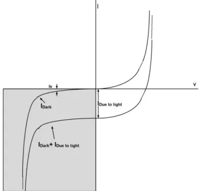
The photodiode current is in opposite direction of the diffusion current. Therefore, as shown in Figure 1.6, illuminating the photodiode with optical radiation shifts the I-V curve to negative values by the amount of the photocurrent (IDue to light).
Figure 1.6. I-V Characteristic curves of a Photodiode under reverse bias – gray region (the upper curve is taken in the dark and the other curve is taken under illumination)
Figure 1.7. shows dark current generation mechanism in simple PN junction:
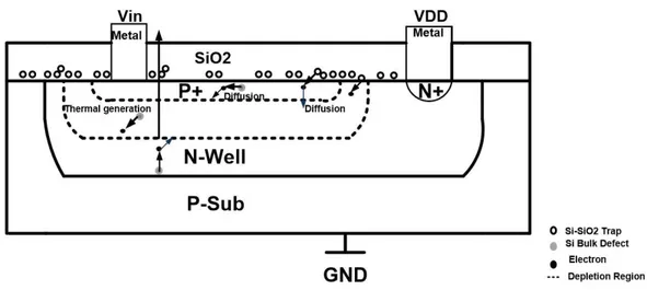
Figure1.7.Dark current generation mechanism in simple P+/N-well photodiode [13]
Since the N-well is connected to VDD and P+ is considered as Vin node in Figure 1.7. , the P+/NW junction is the only active junction. More specifically, only carriers generated by P+/NW diode will be collected as useful information, while the other carriers gathered by the NW/P-sub diode would be swept to the power supplies.
1-4-3 Dark Current Reduction in CMOS Image Sensor
Since the dark current has bad effect on CMOS image sensors performances in the terms of sensitivity and dynamic range, many efforts have been done in order to reduce its effect. Considerable efforts have been made for reducing the dark current by physical modification of the photodetector, such as adding a photogate to the photodiode, adding an n+ reset ring structure [17], surrounding the pixel by a p-well [18] and burying the source follower transistor [19].
Shrinking the feature size technology increases the resolution of image sensors by decreasing the pixels size. Meanwhile, it brings new challenges where using shallow trench isolation (STI) beyond the 0.18um technology significantly and increases the dark current. In deep submicron technologies, STI is used to isolate pixels and components in the pixel from each other. The STI boundaries may have higher defect densities than the substrate, creating a higher density of energy states in forbidden gap between the STI boundaries and the silicon along the Si-SiO2
interface. In order to reduce the dark current due to STI effect, it is possible to increase the distance between photodiode and STI at the expense of losing the fill factor of pixel. The APS 4T structure which includes pinned photodiode has less dark current than pixel with a p-n junction photodiode. In PPD structure, the heavily doped p+ pinning layer significantly reduces the dark current by completely shielding the depletion region of photodiode from touching the bar Si-SiO2 interface.
The most effective way to reduce the dark current is to decrease the depletion width of the photodiode, but small depletion width leads to lower QE. PPD has high QE while having less significant dark current than p-n junction photodiode. However, the pinned photodiode (PPD) based 4-T pixel has some disadvantages, such as a low dynamic range associated with the small well capacity and requires modification of the typical CMOS fabrication process whit additional cost.
Dark current random noise of sensor is mainly reduced by replacing the standard surface mode transistor n-MOS amplifier in the pixel with buried channel source follower. Therefore, the sensor dark current noise in terms of 1/f noise will be reduced by burying the source follower transistor [14].
Reset noise is a dark current random noise which is coming from reset transistor and is modeled as a resistor with thermal noise in ON mode of the reset switch. This thermal noise is sampled and held in the photodiode capacitor after the transistor is OFF. In order to reduce the reset noise voltage, photodiode capacitance (CPD) should be as large as possible. Since the image
performance is reduced by increasing the CPD value, mostly the image sensors suffer from the
reset noise. Recent researches prove that by using the so called soft reset technique, reset noise of 3T pixel could be reduced [20]. In 4T-PPD pixel, the reset noise also could be reduced by using a correlated double sampling CDS structure [14].
1-5 Noise Associate with Dark Current in CMOS Image Sensors
Dark current generates two types of noise: dark current non-uniformity from pixel to pixel, Fixed Pattern Noise (FPN), and temporal noises (reset noise, flicker noise (1/f) and dark shot noise).
1-5-1 Fixed Pattern Noise (FPN)
Two main sources of FPN are: dark current inside the pixel and mismatches due to in-pixel or column level transistors. Pixel-level FPN which is due to transistor parameters mismatches can be eliminated by Correlated Double sampling (CDS) circuits while the mismatch due to column transistors are eliminated in the digital domain during the image processing procedures [14].
1-5-2 Dark Current Shot Noise
Part of electron-hole generation of photo-sensing elements in the absence of illumination which depends on temperature is called dark current shot noise. Dark current shot noise is the dominant source of noise in low light illumination.
VShot = √𝑞𝐼𝑑𝑎𝑟𝑘
𝑡𝑖𝑛𝑡
𝐶𝑃𝐷 (1.10)
where Idark is the average of dark current. The term tint is the integration time. CPD is photodiode capacitance.
The dark current shot noise can be reduced by lowering the temperature, careful pixel layout, a proper transistor size and bias setting [10].
1-5-3 Reset Noise
This noise originates from thermal noise of the reset switch which is often implemented by an NMOS transistor and known as KTC, expressed by
VRST= √𝐾𝑇
𝐶𝑃𝐷 (1.11)
Where K is Boltzmann’s constant (k =1.38E-1023 J/K) and T is the temperature in Kelvin and CPD is photodiode capacitance.
1/f noise is due to lattice defects at the interface of the Si-SiO2 channel of MOS transistor which
is mainly due to the source follower in CMOS image sensors pixel. This noise depends on the gate oxide capacitance, the width and the length of the transistor. Ways to reduce 1/f noise include increasing the size of transistor, reducing the power supply or burying the source follower transistor.
1-6 Leakage in MOSFET
In CMOS image sensor structure different MOS switches are used for different purposes which are described in this chapter. Leakage from switches can add large distortion effect in readout signal. First, different sources of leakage in MOSFET structure are reviewed then, switches and their leakages are presented.
Over the past decades, MOSFET size has been scaled down continuously. Channel length of MOSFETs have been reduced from several micrometers to tens of nanometers in modern integrated circuits. Small size MOSFETs, below few tens of nanometers bring some problems. They need very low supply voltages and have poorer electrical properties like higher leakage currents, and lower output resistance.
Non-ideal behavior of CMOS switches due to leakage current in OFF operation mode is described in this chapter. The main sources of MOSFET leakage currents in deep submicron (DSM) process circuits are: Sub-threshold conduction current (ISUB), gate direct tunneling
current (IG), gate-induced drain leakage current (IGIDL) and reverse-biased junction leakage
current (IREV) as shown in Fig. 1.8. Amongst all the leakage current components, sub-threshold
leakage is the most dominant component [21, 22]. Various techniques have been developed for reducing the sub-threshold leakages in MOSFET transistors.
Figure 1.8. Leakage current components in an NMOS transistor [22] 1-6-1 Reverse-biased junction leakage current (IREV)
The leakage through the source or drain to substrate of the reverse-biased diodes when a transistor operates in OFF mode is called reversed-bias junction leakage. The magnitude of junction leakage depends on the area of the drain or the source diffusion and the density of leakage current is determined by the process technology [23].
1-6-2 Gate-Induced Drain Leakage (GIDL)
Gate-induced drain leakage (GIDL) is caused by band to band-tunneling in the drain region underneath the gate which is very sensitive to the gate oxide thickness, the drain concentration, the lateral doping gradient, and the applied drain-to-gate voltage [22]. When the gate is at zero or negative voltage and the drain is at the supply voltage level, there can be a dramatic increase of avalanche multiplication and band-to-band tunneling. Minority carriers underneath the gate are swept to the substrate, creating GIDL current. GIDL is defined as:
𝐼𝐺𝐼𝐷𝐿= AEs × 𝑒 −𝐵 𝐸𝑠 ⁄ (1-12) 𝐴 = 𝑞2𝑚𝑟 1 2 ⁄ 18.л.ℎ2𝐸 𝑔𝑎𝑝 3 2 ⁄ (1-13) 𝐵 =л 𝐸𝑔𝑎𝑝 3 2 ⁄ 𝑚 𝑟 1 2 ⁄ 2√2.𝑞.ℎ (1-14)
Egap is the direct energy gap of silicon (∼1.12 eV), h is 1/2 π times the Planck’s constant, mr =
0.2 m0 (a silicon effective mass), Es is the vertical electric field at the silicon surface, and q is the electronic charge which is equal to 1.6 E-19 C. Thinner oxide Tox and higher supply voltage Vdd
increase GIDL. GIDL is also referred to as surface band-to-band tunneling leakage [23, 24].
1-6-3 Gate Direct Tunneling (IG)
The gate direct tunneling leakage flows from the gate through the “leaky” oxide insulation to the substrate. The magnitude of IG decreases exponentially with the gate oxide thickness and the supply voltage. The high-K gate dielectric reduces direct tunneling current and is required to control this component of the leakage current for low standby power devices [25].
1-6-4 Sub-threshold Leakage (ISUB)
Sub-threshold leakage is the current from source to drain when the MOSFET is in OFF mode and this current is due to diffusion of minority carriers in the MOSFET channel when the 𝑉𝑔𝑠is less than the threshold voltage [21]. 𝐼𝑆𝑈𝐵 is calculated using the following formula:
𝐼𝑆𝑈𝐵= µ0𝐶𝑜𝑥(𝑊 𝐿) (𝑉𝑇) 2 𝑒1.8 𝑒𝑉𝑔𝑠−𝑉𝑡ℎ0− ɳ𝑉𝑑𝑠−𝛶𝑉𝑠𝑏𝑛𝑉𝑇 (1- 𝑒−|𝑉𝑑𝑠|𝑉 𝑇 ⁄ ) (1.15)
where W and L are the width and length of transistor, Cox is the gate oxide capacitance, µ is the carrier mobility, γ is the linearized body effect coefficient, η is the is the drain-induced barrier lowering (DIBL) coefficient, VT is the thermal voltage and n is the sub-threshold swing coefficient.
The magnitude of the sub-threshold current is a function of the temperature, supply voltage, device size, and the process parameters, such as threshold voltage (Vth) which plays the dominant role.
By shrinking the size of the technologyVth of the transistor is decreased [26]. The threshold voltage depends on four parameters: VSB, doping, process and temperature.
𝑉𝑇𝑁= 𝑉𝑇0+ 𝛶(√|𝑉𝑆𝐵− 2𝜑𝐹| − √|2𝜑𝐹|) (1.16) where VT0 is the threshold voltagefor zero substrate bias, 2𝜑𝐹, the surface potential, VSB, the source to body substrate bias.
In addition to parameters optimization, changes in circuit configuration were presented for reducing the sub-threshold leakage current, such as stack effect, dual and multi-threshold voltage techniques [27, 28].
From the above discussion, we see that ISUB, IREV and IGIDL increase with VDB. Since the transistor gate must be at a high potential with respect to the source and substrate for this current to flow, the IG is not a component of the OFF current. Among the three components of IOFF, ISUB is clearly the dominant component [29].
Figure 1.9 shows the leakage current contributions of OFF mode MOSFET in different deep submicron (DSM) technologies and it shows the dominant of sub-threshold leakage in larger technologies [30]
Figure 1.9. Leakage in different bulk technologies [31]
1-7 Summary
This chapter presented a brief overview of CMOS image sensors. The important characteristics of image sensors, especially the dark current, have been described. Different technics of reducing the dark in CMOS image sensor were reviewed. At the end of the chapter leakage current in MOSFET has been explained. In the next chapter, the new CMOS image sensor structure will be proposed for compensating the dark current effect by considering the effect of MOSFET's leakage on operation of the proposed circuit.
CHAPTER 2 DESIGN OF AN IMAGE SENSOR PROTOTYPE
In this chapter the leakage of MOSFET switches is thoroughly described by simulating and analyzing a sample-and-hold circuit. Then, the structure for compensating the effect of dark current in CMOS image sensors is presented. Afterward, optimization techniques for eliminating the leakage current effect of CMOS switches in the proposed design are described. At the end a subtractor circuit is introduced for subtracting the output of a dummy pixel form a pixel being readout to complete the dark current compensation circuit.
2-1 MOS Switches
2-1-1 Sample-and-Hold Circuit
In this section, we compare and analyze the leakage sources in Transmission Gate (TG) switch by simulating a sample-and-hold circuit.
A simple sample-and-hold circuit is composed of a MOS switch and a hold capacitor. This circuit is suffering from some non-idealities behavior which makes the capacitor voltage to discharge during the hold mode due to MOSFET leakages, clock feedthrough and charge injection effects. As it is shown in Figure 2.1, the TG switch is used instead of a single MOS switch in order to reduce the effect of channel charge injection and clock feedthrough.
Figure 2.1 Sample-and-Hold circuit
The leakage current of the switch discharges the capacitor to input signal Vin, VDD or VSS values during the hold mode of S/H operation. This distortion could be reduced by increasing the capacitor value or decreasing the sampling time of the switch.
Figure 2.2 shows the distortion in the voltage of hold capacitor which is discharged during the hold mode due to different sources (Vin , VDD or VSS). Figure 2.2.b and c show the S/H output which has junction leakages respectively through VDD and VSS and Figure 2.2.d shows the S/H output which has the sub-threshold leakage and discharges the capacitor to Vin value during the hold mode.
Figure 2.2. Sample-and-Hold output with various leakages [32]
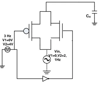
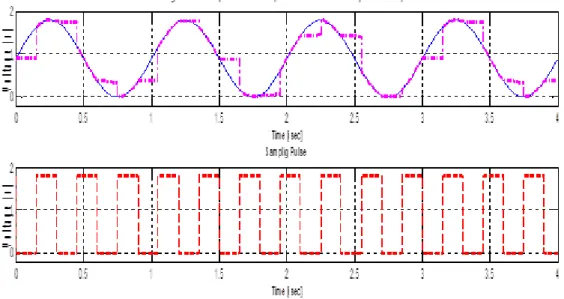
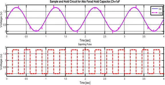
As mentioned before, the dominant leakage of a switch is the sub-threshold current which discharges the capacitor to the input signal value [32]. We are going to show this fact by simulating the circuit of Figure 2.3. This circuit is simulated with an input sine wave (Amp= 0-1 V, f=1 Hz) and hold capacitors in the atto, femto, pico and nano Farad ranges.
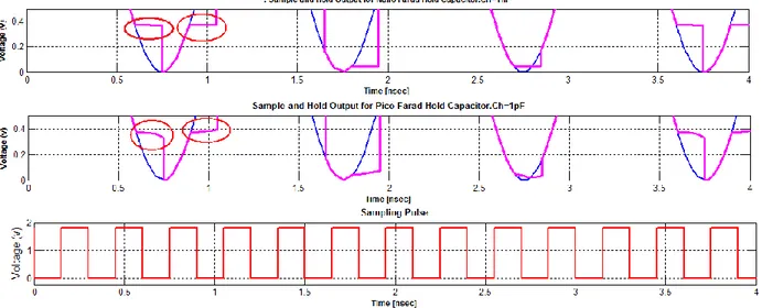
Figure 2.4,5,6,7 show the distortion in the output of a sample-and-hold circuit due to the sub- threshold leakage current. By comparing the graphs in the Figures 2.4,5 and 2.6,7, we see that for femto and atto values of the hold capacitor the sub-threshold leakages current is significant but for larger values of the hold capacitor (pico and nano Farad) the sub-threshold leakage is negligible.
CH ` 3 Hz V1=0V V2=4V Vin, V1=0,V2=2, 1Hz
Figure 2.3. Simple-and-Hold circuit
Figure 2.5. Sample-and-Hold output for Pico Farad hold capacitor.CH=1pF
Figure 2.6. Sample-and-Hold circuit for Femto Farad hold capacitor,CH=1fF
0 0.5 1 1.5 2 2.5 3 3.5 4 0 0.5 1 1.5 2 Time [sec] V o lt a g e ( v)
.Sample and Hold Output for Femto Ampere Hold Capacitor.Ch=1fA
0 0.5 1 1.5 2 2.5 3 3.5 4 0 0.5 1 1.5 2 Time [sec] V o lt a g e ( v) Sampling Pulse Vin Vch
Figure 2.7. Sample-and-Hold circuit for Atto Farad hold capacitor, CH=1aF
The clock feedthrough of S/H circuit which is shown in Figure 2.8 has been calculated according to equation (2.1). The equation shows that the value of the clock feedthrough depends on the clock amplitude and the hold capacitor values [33]. Clock feedthrough error appears as glitches at the edge of clock pulses.
Figure 2.8. Calculating feedthrough effect in simple Sample-and-Hold circuit (MOS Switch)
𝚫𝑽𝟎= 𝑪𝒐𝒍 𝑪𝒐𝒍+𝑪𝑳(𝑽𝑯− 𝑽𝑳) (2.1) 0 0.5 1 1.5 2 2.5 3 3.5 4 0 0.5 1 1.5 2 Time [sec] V o lt a g e ( v)
Sample and Hold Circuit for Atto Farad Hold Capacitor,Ch=1aF
0 0.5 1 1.5 2 2.5 3 3.5 4 0 0.5 1 1.5 2 Time [sec] V o lt a g e ( v) Sapmling Pulse Vin Vch
By comparing Figures 2.4,5,6. and 7, we find the small clock feedthrough effect by using a TG switch. The output graphs show significant clock feedthrough effect on circuits with smaller hold capacitors. For example Figure 2.7. shows clock feedthrough errors due to using atto farad range while Figure 2.4 and 2.5 show negligible effect of clock feedthrough error for nano and pico farad range of hold capacitor.
To analyze the operation of a S/H circuit, the switch is modeled as a high resistor in OFF mode and a low resistor in ON mode. It means that the sample-and-hold circuit could be modeled by a simple RC circuit as it is shown in Figure 2.9.
Figure 2.9. Simple RC circuit which models the S/H circuit
The values of 𝑅𝑂𝑁 and 𝑅𝑂𝐹𝐹 of a simple TG switch is deduced by simulating the configurations below.
Figure 2.10.a. Configuration for calculating RON Figure 2.10.b. Configuration for calculating
The 𝑅𝑂𝐹𝐹 of the TG switch is extracted from Figure 2.11. By sweeping the VTEST voltage
source and measuring the current 𝐼𝐹, the value of about 0. 2TΩ is obtained for 𝑅𝑂𝐹𝐹.
Figure 2.11. OFF resistor of TG
As shown in Figure 2.6 and 2.7, in OFF mode the output of the switch tries to follow the input signal value. Since the 𝑅𝑂𝐹𝐹with the value of TΩ range makes the capacitor to charge with time
constant which equals to 𝑅𝑂𝐹𝐹𝐶𝐻 (<1ms) and 1000 times less than hold time (1sec). Thus, the capacitor voltage is discharged by the input source (Vin) due to sub-threshold leakage of the switch during the hold time .For nano Farad values of the capacitor, the constant time is τ =RC>100s which is quite larger than the hold time. So there is no distortion in the output voltage during the hold time as it is shown in Figure 2.4. Figure 2.5. shows a little effect of sub-threshold leakage which affects the hold voltage mode of pico farad capacitor while it doesn’t have effect on nano Farad capacitors. Figure 2.12 shows this effect by scaling Figures 2.4 and 2.5. Red circles in Figure 2.12 shows the effect of sub-threshold voltage on pico and nano Farad hold capacitors. 0.2 0.4 0.6 0.8 1 1.2 1.4 1.6 -10 -8 -6 -4x 10 -12 VRST [V] Io f f ( A ) If VS VRST 0.2 0.4 0.6 0.8 1 1.2 1.4 1.6 -2.1 -2 -1.9 -1.8x 10 11 VRST [V] R e s is t o r ( o h m )
Transmission Gate OFF Resistor
If VS VRST
Figure 2.12 Comparison of the sub-threshold leakage effect of single MOS switch on Nano and Pico Farad hold capacitors
The charge injection effect in the output could be reduced by decreasing the fall time and rise time of the clock pulse feeding MOSFETs’ gates.
2-2 Proposed Circuit Reducing the Effect of Dark Current in CMOS Image Sensor
In this section a circuit for compensating the effect of dark current in CMOS image sensor is proposed. Since differential architecture could not efficiently compensate the non-uniformity noise effects, a feedback configuration which fixes the integrating node of photodiodes and makes uniformity dark current noise is implemented. Pixel architecture is presented and optimized for low level sensing illuminations and number of pixels is expanded for a row of pixel array.
2-2-1 Capacitive Transimpedance Amplfier (CTIA)
A simple integrator circuit is shown in Figure 2.15. which is known as a Capacitive Transimpedance Amplfier (CTIA) [6, 34].
Figure 2.13. Capacitive Transimpedance Amplfier (CTIA)
The circuit is used to convert the photodiode current to voltage. The integrator circuit consists of an amplifier, an integrating capacitor (Cr) located in the negative feedback loop and a reset switch transistor in parallel to the capacitor. Also a readout switch is shown in the figure which is connected to the bus line of the pixel array column.
As mentioned in chapter one, a photodetector produces a current proportional to the amount of incident light which is modeled by a DC current source (IPD). The traditional P+/N-well photodiode is used. Also N-well/P-sub photodiodes could be used by switching to complementary configuration. The typical circuit model of a photodiode is shown in Figure 2.16.
Figure 2.14. The PN junction: A junction capacitance (Cj) and a shunt resistance (RSh) are in
parallel with the other components. Series resistance (RS) is connected in series with all
components in this model
CTIA circuit is operating in “reset” and “integrating” modes. By closing the reset switch, the integrating capacitor is discharged and the op-amp acts as a buffer amplifier. As a result, the output will be equal to 𝑉𝑅𝐸𝐹value; the non-inverting and inverting input of the op-amp:
𝑉𝑅𝐸𝐹 =𝑉+ = 𝑉− (2.2)
The integration phase starts after opening the reset switch. Constant current from the photodiode (𝐼𝑃𝐷) integrates across 𝐶𝑟. Due to feedback and the large amplifier gain, the integration node (inverting input) and the non-inverting input of the op-amp will remain equal to 𝑉𝑅𝐸𝐹. Equation
(2.3) determines the total charge of the capacitor during the integration mode. 𝑡𝑖𝑛𝑡 is the elapsed time from the start of the integration phase.
Q = 𝐼𝑃𝐷 Δ t = 𝐶𝑟 (𝑉REF - 𝑉𝑂𝑢𝑡( 𝑡𝑖𝑛𝑡)) (2.3) Therefore the output voltage of the op-amp during the integration time can be given as
𝑉𝑂𝑢𝑡( 𝑡𝑖𝑛𝑡)= 𝑉𝑅𝐸𝐹 −𝐼𝑃𝐷× 𝑡𝑖𝑛𝑡
𝐶𝑟 (2.4)
So, the output voltage in the integrating time has a negative slope which depends on the intensity of the photodiode current.
Figure 2.15 Integrator circuit output [35]
A circuit using two integrators and two photodiodes is shown in Fig. 2.18. One of the photodiodes is sensitive to the light and generates photo-current and dark-current. The other photodiode is shielded from the light and has only dark current at its output. The circuit is operating in “reset” and “integrating” modes as simple integrator circuit. The output voltage of each op-amp is equal to the simple integrator circuit described before:
𝑉𝑂𝑢𝑡1( 𝑡𝑖𝑛𝑡)=𝑉𝑅𝐸𝐹 −
(𝐼𝐷𝑎𝑟𝑘)
𝐶𝑟 𝑡𝑖𝑛𝑡 (2.5)
𝑉𝑂𝑢𝑡2( 𝑡𝑖𝑛𝑡)=𝑉𝑅𝐸𝐹− (𝐼𝐷𝑎𝑟𝑘+𝐼𝑝ℎ𝑜𝑡𝑜)
Figure 2.16. CTIA interface [36]
In order to decrease the number of transistors in each pixel so that the fill factor is increased, the structure of the two amplifiers in Figure 2.18. can be modified into the more compact amplifier presented in Figure 2.19.
Figure 2.17. Double-Input Double -Output CTIA
The new amplifier has one non-inverting and two inverting inputs as well as two outputs. In Figure 2.19, Vout2 depends on the photo and dark current of the photodiode (IPD=IDark +IPhoto) while Vout1 depends only on the photodiode dark current (IPD=IDark). By subtracting Vout1 from
Vout2 in the integrating phase, the output voltage becomes less dependent on the photodiode dark current:
𝑉𝑂𝑢𝑡2( 𝑡𝑖𝑛𝑡) − 𝑉𝑂𝑢𝑡1( 𝑡𝑖𝑛𝑡)=(𝐼𝐷𝑎𝑟𝑘+𝐼𝑝ℎ𝑜𝑡𝑜)− (𝐼𝐷𝑎𝑟𝑘)
𝐶𝑟 tint=
𝐼𝑝ℎ𝑜𝑡𝑜
𝐶𝑟 tint (2.7)
The number of integrators can be expanded to the number of pixels in a row and leads to a new configuration being a multiple input/output integrator circuit. The symbol of the multi-branch CTIA is shown in Figure 2.20.
Figure 2.18. Multi-Branch differential amplifier [6]
2-2-2 Leakage Current Reduction of Reset Switch
As explained in the first section of this chapter, leakage current from MOSFET switches could have distortion effect on the output of the circuit especially when the switches are in OFF mode. The effect of this leakage is seen during the charge of the hold capacitor in the sample-and-hold circuit. In the proposed circuit, off transistor leakage of MOSFET has an effect on the accumulated charge in the capacitor of the integrator circuit.
When using a single MOS or CMOS transmission gate (TG) as the reset switch in the integrator circuit, the small dark current of the photodetector cannot build any voltage across the capacitor. This is because often the leakage current of the OFF reset switch exceeds the dark current value of the photodiode. When the capacitor starts charging during the integration mode, the built up voltage on the capacitor increases the VDS voltage of OFF Switch which creates the leakage current in OFF reset switch during the integration time. This leakage is trying to discharge the capacitor. . The discharge happens in a smaller time constant than the time needed
for the capacitor to charge with the dark current of the photodiode.
As mentioned before, the sub-threshold leakage is the dominant leakage current contribution in MOSFETs which is a current flowing from drain to source when the MOSFET is in OFF mode. The leakage current and photodiode dark current directions are shown in Figure 2.21.
Figure 2.19. Leakage of CTIA circuit with NMOS reset switch
Various techniques have been presented to reduce sub-threshold leakages in MOSFET transistors. In the integrator circuit, a T-type circuit is used as a reset switch for reducing the sub-threshold leakage current of the switch by putting the Vds of the MOS to zero [35]. As shown in Fig. 2.22, in the T-type switch configuration, the single NMOS switch is replaced by two NMOS switches in series and one NMOS switch connected between a Vb voltage source and the node between NM1 and NM3. Voltage Vb is set close to the integrating node voltage, VREF value. During the integration mode where NM1 and NM3 switches are OFF and NM2 is ON, the node between NM1 and NM3 switches is pulled to Vb through the ON resistor of NM2 transistor. Since the drain of NM1 is connected to Vb, drain-source voltage of NM1 is close to zero and the leakage of NM1 approaches zero. Therefore, the leakage current of the T-type switch is greatly reduced.
Figure 2.20. CTIA circuit with T-type reset switch
During the circuit reset mode, NM1, NM3 are ON and NM2 is OFF. By using the TG switches instead of NM1 and NM3 in the T-type configuration, the channel feed through effect of the switch could be reduced. Also stacking NM1 and NM3 by putting few transistors in series with NM1 and NM3 leads to a smaller drain source voltage for the transistors. Therefore, according to (1.15), with a smaller Vds, the sub-threshold leakage flowing through the stacked-series transistors will be reduced [37]. Since the design aims at reducing the number of transistors in a pixel, the simple configuration of the T-type switch with three transistors was considered.
The leakage current of the single MOS switch is in the range of pico-amperes while the leakage current of the T-type switch can be below 1 fA [35, 37-39].
2-3 Actual Implementation
The multi-branch differential amplifier for compensating the effect of dark current in CMOS image sensors is presented in [6]. The dummy pixel and the non-shielded pixel of the multi-branch amplifier are shown in Fig. 2.23. In the dummy pixel of the circuit, the capacitor cannot be charged using the small dark current value of the photodetector during the integration time (when the TG switch is OFF) because the time constant responsible for charging the capacitor
through the OFF switch of path 2 is smaller than the time needed to charge the capacitor via the photodiode dark current. Also in the non-shielded pixel of Fig. 2.23, the capacitor is discharged through the OFF resistor of the TG switch (through path 1) while being charged by the photodiode current. In the proposed architecture, the TG switch in the non-shielded pixel is replaced by a T-type switch with a smaller leakage current. The replaced switch doesn’t prevent the capacitor from being charged by the photodiode dark current since the switch leakage is less than the photo diode dark current. However, replacing the TG switch by the T-type switch in the dummy pixel cannot solve the switch’s leakage problem because in this configuration, the drain-source voltage of the transistors in the T-type switch is not equal to zero during the integrating mode of the circuit. From Fig. 2.22, we found that an effective low-leakage T-type switch can be implemented only when it is placed in the feedback path of the circuit. Therefore, the configuration of the shielded dummy pixel should be modified to a new structure with feedback.
Figure 2.21. Dark current compensation circuit of [6]
Changing the configuration of the circuit in [6] leads to a new structure of multiple-input multiple-output integrator which is shown in Fig. 2.24. In proposed design, one dummy pixel is shared with an entire row of pixels and its dark current is subtracted from the output voltage of each pixel in a row. Therefore, the subtractor circuit gives an output voltage where the
contribution of the photodiode dark current has been greatly reduced. The subtractor circuit is implemented in a column amplifier at the bottom of the pixel array. Implementing a complete differential amplifier in each pixel reduces the fill factor and increases power consumption. The proposed solution is achieved by implementing multiple-input multiple-output differential amplifier; the amplifiers would have one non-inverting and a several inverting inputs as shown Fig. 2.24. The number of inverting inputs is equal to the number of pixels in a row plus a dummy pixel. Unlike the previous configuration, the new setting provides constant voltages across the reset T-type switch.
Since the photodiode has fixed depletion region width due to the feedback configuration, photodiode capacitance (CPD) has a constant value. Each photodiode is modeled with a current
source in parallel with a constant photodiode capacitor.
Figure 2.22. Multiple-Input Multiple-Output Differential Capacitive Transimpedance Amplifier.
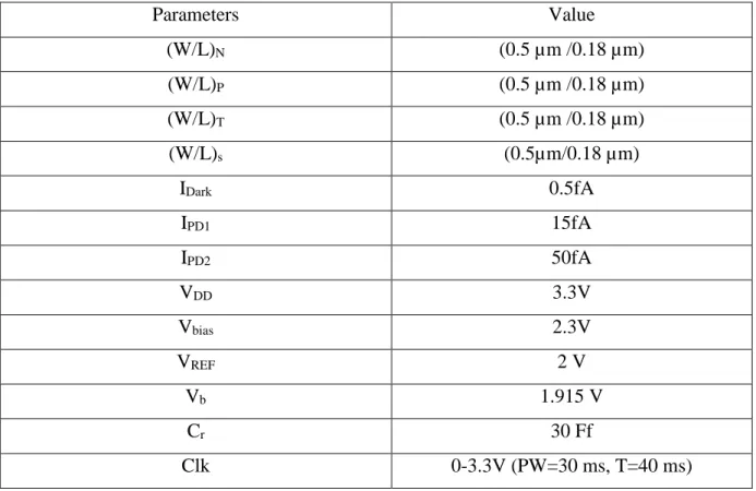
Table 2.1. Parameter values of the circuit of Figure 2.24. Parameters Value (W/L)N (0.5 µm /0.18 µm) (W/L)P (0.5 µm /0.18 µm) (W/L)T (0.5 µm /0.18 µm) (W/L)s (0.5µm/0.18 µm) IDark 0.5fA IPD1 15fA IPD2 50fA VDD 3.3V Vbias 2.3V VREF 2 V Vb 1.915 V Cr 30 Ff Clk 0-3.3V (PW=30 ms, T=40 ms) 2-4 Subtractor Circuit
Subtractor circuit is used for subtracting non-dummy pixels’ output from dummy pixel. The schematic of a subtractor circuit is shown in Fig 2.25 which has a symmetrical structure [40]. The bias current of the circuit is obtained by M1 and M2 which operate as a current mirror source. The subtractor circuit has three inputs and one output. The three inputs are VBG1, VBG2 and Vx. Since M1 and M2 operate as current mirror source, I1 and I2 are equal. M3 and M4 are driven by the constant current I1 while M5 and M6 are driven by the constant current I2. The gates of M3 and M4 are connected to VBG1 and VBG2 respectively. VBG1 is chosen to be larger than
VBG2. The gate of MOS transistor M6 connects to the constant voltage which keeps M6 in saturation region. The drain of MOS transistor M5 is the output of the subtraction circuit. Since M8 and M9 forms the current mirror circuit, ID4=ID5. From I1=I2, we get ID3=ID6. Based on the
relationships between the gate to source voltages and the drain currents, we can easily find that the output voltage of the subtraction circuit is given by the following equeation:
Vsub= Vx-(VBG1-VBG2) (2.8)
Figure2.23 Subtractor circuit [40]
Table 2.2 shows the parameter values of subtractor circuit:
Table 2.2 Parameter values of subtractor circuit:
(W/L)(7,8,9,10) (0.6µm/0.18µm)
(W/L)(1,23,4,5,6) (0.5µm/0.18µm)
VDD 3.3V
Vx 2V
2-5 Summary
In the chapter a new architecture for compensating the effect of dark current in CMOS image sensors has been proposed. The proposed design which is presented in Figure 2.24 has the ability to sense low level illuminations by compensating dark current. It employs T-type switches which have reduced OFF transistor leakage current than regular MOS or TG switches.
CHAPTER 3 POST-LAYOUT SIMULATIONS AND RESULTS
In this chapter layout and post-layout simulation of designed structure is presented. Also Monte Carlo simulation has been done in order to analyze the effect of manufacturing process on the proposed design.
3-1 Simulation Results
3-1-1 Simulation result with three pixels
Simulation results of the circuit in Fig. 2.24, are presented in Fig. 3.1. According to equation (2.5), the graph shows that during the integration time the output voltage of each pixel has a slope which depends on the total photodiode current (IPD=IDark +IPhoto). During the reset mode, the output is forced to 𝑉𝑅𝐸𝐹 because of the differential amplifier configuration. The integration and reset times are both selected to be 30ms and 10ms respectively.
All photodetectors in Fig. 2.24 are modeled by constant current sources [6, 15]. In this simulation, the current of the dummy pixel is set to IDark =0.5 fA (Table 3.1) and the photodiode current of the other pixels are chosen to be IPD1 =15 fA and IPD2 =50 fA. The integrating capacitor (Cr) is chosen to be 30fF.
![Figure 2.18. Multi-Branch differential amplifier [6]](https://thumb-eu.123doks.com/thumbv2/123doknet/2339101.33518/51.918.295.645.129.398/figure-multi-branch-differential-amplifier.webp)
![Figure 2.21. Dark current compensation circuit of [6]](https://thumb-eu.123doks.com/thumbv2/123doknet/2339101.33518/54.918.185.732.513.886/figure-dark-current-compensation-circuit.webp)