Any correspondence concerning this service should be sent to the repository administrator:
[email protected]
Identification number: DOI: 10.1016/j.ceramint.2013.04.060
Official URL:
http://dx.doi.org/10.1016/j.ceramint.2013.04.060
This is an author-deposited version published in:
http://oatao.univ-toulouse.fr/
Eprints ID: 13982
To cite this version:
Valdez-Nava, Zarel and Guillemet-Fritsch, Sophie and Ferrato, Marc and
Kozako, Masahiro and Lebey, Thierry
Co-fired AlN–TiN assembly as a new
substrate technology for high-temperature power electronics packaging
. (2013)
Ceramics International, vol. 39 (n° 8). pp. 8743-8749. ISSN 0272-8842
O
pen
A
rchive
T
oulouse
A
rchive
O
uverte (
OATAO
)
OATAO is an open access repository that collects the work of Toulouse researchers and
makes it freely available over the web where possible.
Co-fired AlN–TiN assembly as a new substrate technology for
high-temperature power electronics packaging
Zarel Valdez-Nava
a,b,n, Sophie Guillemet-Fritsch
c, Marc Ferrato
d, Masahiro Kozako
a,b,e,
Thierry Lebey
a,baUniversité de Toulouse, UPS, INPT, LAPLACE (Laboratoire Plasma et Conversion d'Energie), 118 route de Narbonne, F-31062 Toulouse Cedex 9, France bCNRS, LAPLACE, F-31062 Toulouse, France
cInstitut Carnot CIRIMAT, Université Paul Sabatier, UMR CNRS 5085, 118 route de Narbonne, 31062 Toulouse Cedex 9, France dBoostec, Zone Industrielle, 65460 Bazet, France
eDepartment of Electrical Engineering and Electronics Faculty of Engineering, Kyushu Institute of Technology, 1-1, Sensui-cho, Tobata-ku, Kitakyushu-shi, Japan
Abstract
New wide-band gap semiconductors (SC) for power electronics such as SiC, GaN and diamond will allow higher power densities, leading to higher operating temperatures. However, the surrounding materials will also undergo an increase in temperature, meaning that a parallel effort is needed in SC packaging technologies research. One of the essential components, the substrate, is used to insulate electrically the SC from the rest of the system, drain the generated heat and provide a path to connect the SC to the rest of the system. Direct bonded copper (DBC) and active metal-brazed (AMB) substrates have limited temperature and cycling operation, owing to the large differences in the thermal expansion coefficients between the ceramics and the metals. In this work we propose a new and original substrate technology based on two co-sintered ceramics: an insulating ceramic (AlN) and a conductive one (TIN). The microstructure, the chemical compatibility and the electrical properties indicate that the proposed substrate could operate at a temperature above 200 1C the current substrate technologies, which makes it particularly attractive for high-temperature power electronics applications.
Keywords:Ceramic substrates; SPS sintering; High-temperature power electronics
1. Introduction
The use of wide band gap semiconductors such as SiC, GaN and diamond will constitute a real breakthrough in power electronics in the near future. The unique properties of these semiconductors will allow the development of high switching speed, high voltage and high-temperature applications. “High-temperature power electronics” is generally used to describe systems able to work in harsh environments mainly in “onboard applications” such as automobile, aircraft and space exploration[1]. In some cases, high temperature is associated with the environment itself (for example, when the converter is located in the vicinity of a thermal engine) but in other cases, it is only related to the
increase of the power density owing to power integration[2]. For some targeted applications, the weight is often a key issue. The high-temperature capabilities and low loss operation of wideband gap semiconductor devices enables them to be used with simplified and more economical cooling systems. In contrast to silicon-based systems that need sophisticated cooling systems (e.g., fluid circulation, loop heat pipes, etc.) classical air, or forced air heat-dissipating systems could be envisaged.
Nevertheless, the opportunities offered by these components might be limited because their packages are inadequate as regards insulation, interconnection and thermal management under high-temperature operations and environments. The future of high-temperature power electronics is dependent on the development of appropriate packaging.
Considering today's power modules, their packaging com-prises a stack of different conductive and insulating materials. The choice of the materials is simply a trade-off between their
http://dx.doi.org/10.1016/j.ceramint.2013.04.060
n
Corresponding author at: Université de Toulouse, UPS, INPT, LAPLACE (Laboratoire Plasma et Conversion d'Energie), 118 route de Narbonne, F-31062 Toulouse Cedex 9, France. Tel.: +33 561558387.
mechanical, thermal and electrical properties such as their thermal expansion coefficients (CTE), their thermal and/or electrical conductivity, their dielectric strength, their mechan-ical fatigue, their tracking index (CTI) [3] and in the case of high voltage applications, their Partial Discharge Inception Voltage (PDIV) [4]. For high-temperature applications, most structures and materials used today are not suitable. In fact, the silicone gel or the epoxy resin generally used to encapsulate the dies and to ensure the dielectric strength of the power module cannot be used for operating temperatures higher than ∼250–300 1C. The same constraint is true for the die attach-ment materials and the interconnection technologies that must be reconsidered. Even the use of Direct Bond Copper (DBC) substrates, which are today the most important circuit board for multichip high power semiconductor devices, might be ques-tionable as regarding their reliability in the high temperature range. More particularly, their behavior during thermal cycling has been proven to be a key issue. Under severe thermo-mechanical stress or when thermal cycling is expanded to higher temperature range their reliability becomes unsatisfac-tory [5,6]. Cracks could be initiated near the interface of the ceramic layer, and delamination of the copper from the base ceramic (whether it is Al2O3 or AlN) is often observed [6–9] and thus, ways to increase their reliability have been studied[7,8].
DBA (Direct Bond Aluminum) substrate often appears as a possible substitution solution. In fact owing to their interesting mechanical properties (the low elastic modulus of aluminum, lower yield stress than copper) it reduces the thermomechani-cal stresses and fatigue at the interface with the ceramic material. Nevertheless, the main drawback in using DBA is the aluminum oxide layer formed on top of the aluminum surface
[10].
In this paper, we propose a completely new approach for substrate technology using a new type of structure consisting of TiN/AlN/TiN cofired ceramics. This “all-ceramic” approach has not been developed for substrate technologies. As TiN is well known to be a conductive material and AlN an insulating one, the proposed structure could be used in a very large temperature range (up to 500 1C). Last, their co-sintering realized thanks to a Spark Plasma Sintering (SPS) system ensuring both the quality of the interface and the compatibility of the materials. The principle of the realization and the characterization of this structure are described and discussed in the following.
2. Experimental procedure
Two different and commercially available starting powders of aluminum nitride (Atochem) and titanium nitride (Stark) are used. X-ray diffraction (Bruker AXS D4) and laser granulo-metry (Malvern Nanosizer ZS) allow the determination of the structure and the grain sizes of the powders. The grain morphology and the agglomeration state are observed thanks to scanning electron microscopy (FEG-SEM Jeol JSM 6700F). The main intrinsic properties of AlN and TiN are reported
inTable 1. For comparison the properties of copper are shown as well.
SPS is a recently developed technique known to be very effective for the densification of nanostructured powders without significant grain growth during the sintering process. In fact, a consolidation at lower temperatures for shorter period is possible in comparison with other conventional sintering methods. SPS is a process combining conventional Electric-Current Sintering and Hot Uniaxial Pressing. The electric current is applied to a specimen in pulse-form and the specimen is heated both by resistance heating of the specimen itself and the conductive die mold (usually graphite). SPS apparatus (Sumitomo 2080) is used to sinter the ceramics. This system allows for simultaneous measurement of the tempera-ture, the applied currents, surface temperature of the graphite matrix as well as the on-line measurement of the vertical displacement of the piston. The powders are introduced inside a graphite matrix 15 mm in diameter. A sufficient amount of powder is placed to obtain samples with a maximum thickness of about 10 mm at 100% Dth. For all the experiments, a pressure of 100 MPa is applied during sintering. Before attempting the realization of the co-sintered AlN/TiN ceramics, a series of SPS sintering experiments were carried out, to determine the thermal profile that allows the full densification for each material. Furthermore, we could determine the impact of the process on the main electrical properties of AlN and TiN.
After sintering, the surface and the fracture of the ceramics are observed both optically and by electron microscopy. Electrical characterization for conductive TiN is performed using a combination of a Keithley 2410 Sourcemeter and a Keithley 2182A Nanovolmeter in a four-probe configuration (Micrometrics HTC). A geometrical correction is applied to the measured resistance values to estimate the volumetric resistivity of TiN [11]. A broadband impedance analyzer (Novocontrol Alpha-A) is used in the temperature range of 25–330 1C and from 100to 106Hz to determine the dielectric properties of the AlN and of the final assembly.
3. Experimental results
3.1. Powder characterization
The MEB-FEG images for both powders are shown inFig. 1. AlN powders have monomodal dispersion centered at 1.9 mm. TiN powders exhibit a bimodal distribution, with small particles starting from 50 nm up to particles of 20 mm and an average grain size of 2.6 mm (Fig. 2). X-ray diffraction results show
Table 1
Summary of the main intrinsic properties of the materials.
Intrinsic properties AlN TiN Cu Thermal conductivity (W K−1m−1) 180 66 400 Electrical resistivity (mΩ cm) 1020 22 1.6 Coefficient of thermal expansion (20–100 1C) (10−6K−1) 5.6 8 17
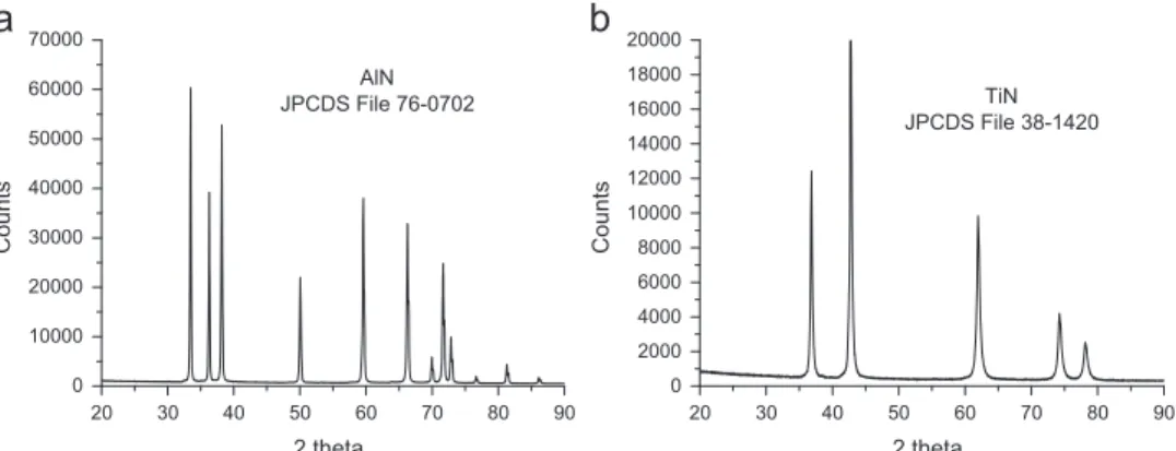
monophased crystalline powders corresponding to JCPDS file 76-0702 for AlN and JCPDS file 38-1420 for TiN (Fig. 3).
3.2. Sintering results
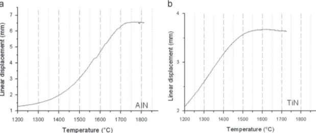
The preliminary sintering of each powder allows the deter-mination of the optimal sintering conditions for AlN on the one hand, and TiN on the other. From the linear displacement
of the SPS piston (Fig. 4), it can be observed that the densification is nearly completed at 1600 1C for TiN and 1750 1C for AlN. For AlN, a dwell at 1800 1C is necessary to obtain a density of 97% of the theoretical density. Therefore, this last temperature (highest between AlN and TiN) was retained to co-sinter the ceramic powders.
Unfortunately, the direct co-sintering of TiN and AlN produce samples presenting mechanical cracks on the TiN side, whatever
Fig. 1. FEG-SEM micrographs of (a) AlN powder, and (b) TiN powder.
Fig. 2. Particle size distribution of (a) AlN powder and (b) TiN powder.
20 30 40 50 60 70 80 90 0 10000 20000 30000 40000 50000 60000 70000 Counts 2 theta AlN JPCDS File 76-0702 20 30 40 50 60 70 80 90 0 2000 4000 6000 8000 10000 12000 14000 16000 18000 20000 Counts 2 theta TiN JPCDS File 38-1420
the process parameters. This is not surprising, because there is a difference in their thermal expansion coefficients (CTE) (Table 1). In order to reduce the stress owing to the differences in the coefficient of thermal expansion between the two materials (see
Table 1), an interface composed of a mixture of AlN and TiN powders was inserted between the pure powders. This composition-graded interface acts a matching interphase between the pure materials (Fig. 5). In order to achieve these layers, raw powders are mixed in a planetary ball mixer using zirconia balls (Turbula). The first layer of TiN powder is placed into the SPS matrix and then a series of inter-layers of 10 wt% increments are used between the AlN and TiN layers. As an example, for a 8 mm-thick sample, the matching layer mm-thickness is around 500 mm, i.e. around 6% of the total thickness. Finally, a layer of AlN powder is placed in the mold before sintering the powders in a single cycle. After sintering, optical inspection showed no cracks in the joined AlN–TiN substrate (Fig. 6).
A SEM-FEG micrograph of the interlayer is shown in
Fig. 7, where AlN (dark) and TiN (clear) are clearly identifi-able. The use of SPS sintering, with a very short cycle ( o 30 min), avoids the formation of an intermediate phase. X-ray diffraction analysis shows no detectable phases other than AlN and TiN. This indicates that there is no significant interdiffusion between the AlN and the TiN phases.
3.3. Electrical characterization
We verified that the assembly of TiN/AlN ceramics could effectively be used in high-temperature power electronics applications, and to fill in the function a metallized substrate with a conductive and insulating surface. The broadband dielectric properties of the aluminum nitride and the electrical conductivity of titanium nitride issued from the SPS sintering were determined at high temperatures.
3.3.1. Electrical conductivity of titanium nitride vs. temperature
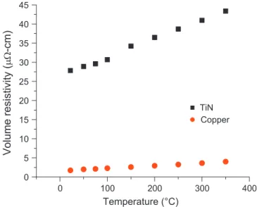
“Conventional” titanium nitride has a volume resistivity of 22 mΩ-cm at room temperature (Table 1), which is 10 times that of copper. The resistivity of TiN samples obtained by SPS
is approximately 27 mΩ-cm. Therefore the SPS process does not degrade this property. The variation of the volume resistivity with temperature both of TiN and of copper is plotted in Fig. 8. Both copper and TiN exhibit an increase in resistivity of ∼60% between room temperature and 375 1C. It is important to note that the values of copper in this figure are estimated from the literature using the temperature coeffi-cient of resistivity and only that pure copper is considered and not an oxidized form. Although, this is the ideal behavior and it cannot be applied in air. As a matter of fact, Wang et al.[12]
show that pure copper, when heated in air up to 350 1C, becomes oxidized and presents a surface oxide thickness of 2 mm after heating it for only 16 min. In contrast, TiN can withstand temperatures up to 400 1C in air with a linear change of resistivity. We observed no apparent oxidation of the surface of the sample because the measured values remained constant when measuring different zones at the surface of the sample (the four-probe is raised and lowered in different sample zone). The resistivity, measured at the surface is completely reversible when the temperature is decreased to room temperature.
3.3.2. Impedance spectroscopy of AlN
Broadband impedance measurements are performed on the following samples: AlN sintered by SPS and TiN/AlN assembly sintered by SPS. For sake of comparison, a com-mercial AlN AMB (Aluminum Metal Brazed) sample is also measured. The comparison among the different configurations allows the determination of the main dielectric properties of the interface and whether this assembly could be used in the targeted applications.
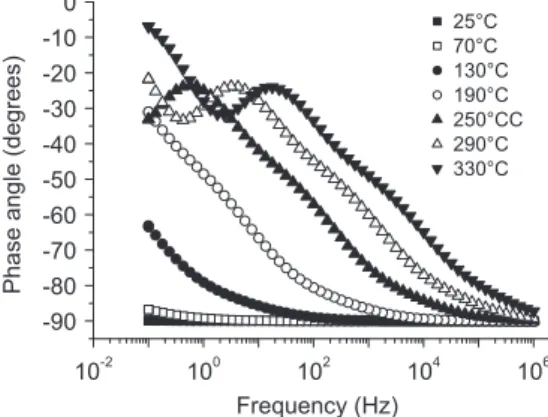
Impedance measurements (∣Z∣) of AlN sintered by SPS (Fig. 9) confirm that this material behaves as a dielectric over a broad temperature and frequency range. The samples present a decrease of two orders of magnitude, ∣Z∣ falling from 1011 at room temperature at 0.1 Hz to less than 1010 at 330 1C. The observed behavior, of tending to a resistive-like compartment (Fig. 10) has been observed in a large number of insulating materials that are claimed to be “semi-insulating” [13,14].
When an interface exists and regardless of the nature of the conductor used (Fig. 11 TiN in the AlN/TiN assembly and
Fig. 13 Aluminum in a AMB commercial substrate), the
electrical response of the system is degraded in the low frequency and high temperature range (see, for example, the phase changes of these different samples given inFigs. 10, 12 and 14). In this case, the impedance decrease is about four orders of magnitude for the samples presenting an interface.
The explanation of these latter phenomena appears to be more complex because the phase angle changes in a
non-continuous way when the temperature is increased and when the frequency is decreased. The only possible explana-tion is related to the existence of an interface between the conductive material and the insulating one. By comparing the results of Figs. 10 and 12, it seems that the existence of the interlayer tends to modify the transition from a pure insulating material to a semi-insulating one, contrary to what is observed for the commercial AMB sample.
Fig. 5. Iliustration of the junction between AlN and TiN, with a concentration gradient. Backscattered electrons SEM-FEG images show AlN-phase (dark) and TiN-phase (bright) (Bar ¼10 mm).
Fig. 6. Sintered substrate 15 mm in diameter. Top side is TiN.
Fig. 7. SEM-FEG backscattered electrons image of an interlayer of AlN–30% TiN mixture after sintering.
Fig. 8. Changes of the volume resistivity of TiN and Cu vs. temperature up to 375 1C (copper values are estimated from the literature).
Fig. 9. Impedance as a function of frequency and temperature for SPS sintered AlN.
4. Conclusions
A novel and original “all-ceramic” assembly has been elaborated by SPS sintering in order to be used for high-temperature power electronics applications, which comprises an insulating ceramic AlN and a conductive one, TiN.
The difference in CTE between the two materials leading to mechanical failure after co-sintering could be overcome by inserting an interface of a composition gradient of TiN and AlN. The as-prepared sandwich shows an interesting dielectric
behavior, similar to the commercial AMB substrates. The great advantage of having an “all-ceramic” assembly for future applications is the high working temperatures attainable by both of the materials. The proposed substrate technology might have advantages regarding thermal cycling behavior and the related thermo-mechanical ageing, owing to the low CTE of the ceramics, compared with the CTE of both copper and aluminum. Further work must now be undertaken to demon-strate this assumption.
References
[1] P.G. Neudeck, R.S. Okojie, L.Y. Chen, High-temperature electronics—a role for wide bandgap semiconductors?, Proceedings of the IEEE 90 (2002) 1065
[2] J. Yin, Z. Liang, J.D. van Wyk, High temperature embedded SiC chip module (ECM) for power electronics applications, IEEE Transactions on Power Electronics 22 (2007) 392.
[3] R.W. Johnson, C. Wang, Y. Liu, J.D. Scofield, Power device packaging technologies for extreme environments., IEEE Transactions on Electro-nics Packaging Manufacturing 30 (2007) 182.
[4] T. Lebey, D. Malec, S. Dinculescu, V. Costan, F. Breit, E. Dutarde, Partial discharges phenomenon in high voltage power modules, IEEE Transactions on Dielectrics and Electrical Insulation 13 (2006) 810. [5] L. Dupont, K. Zoubir, S. Lefebvre, S. Bontemps, Effects of metallization
thickness of ceramic substrates on the reliability of power assemblies under high temperature cycling, Microelectronics Reliability 46 (2006) 1766.
Fig. 10. Phase angle as function of frequency and temperature for SPS sintered AlN.
Fig. 11. Impedance as a function of frequency, for various temperatures for SPS sintered TiN/AlN assembly.
Fig. 12. Phase angle response as a function of frequency for various temperatures for SPS sintered TiN/AlN assembly.
Fig. 13. Impedance as a function of frequency, for various temperatures for a commercial AlN/Al substrate (AMB).
Fig. 14. Phase angle as a function of frequency and various temperatures for a commercial AlN/Al substrate (AMB).
[6]Y. Yoshino, H. Ohtsu, T. Shibata, Thermally induced failure of copper-bonded alumina substrates for electronic packaging, Journal of the American Ceramic Society 75 (1992) 3353.
[7]J. Schulz-Harder, IMAPS Nordic, HPS DBC Substrates for High Reliable Applications, Poster at IMAPS Nordic, Oslo, Norway, 2001.
[8]J. Schulz-Harder, Reliability of direct copper bonded (DBC) substrates, in: Proceedings of ISHM 11th European Microelectronics Conference, Venice, Italy, 1997.
[9]J. Schulz-Harder, Advantages and new development of direct bonded copper substrates, Microelectronics Reliability 43 (2003) 359. [10]D.A. Weirauch, Ceramic Microstructures'86, Plenum, New York, 1987,
p. 329.
[11] Y.G. Gogotsi, Particulate silicon nitride-based composites, Journal of Materials Science 29 (1994) 2541.
[12] W. Wang, W. Lanford, S. Murarka, Completely passivated high conductivity copper films made by annealing Cu/Al bilayers, Applied Physics Letters 68 (1996) 1622.
[13] S. Diaham, M.-L. Locatelli, T. Lebey, Conductivity spectroscopy in aromatic polyimide from 200 to 400 1C, Applied Physics Letters 91 (2007) 122913.
[14] S. Diaham, M.-L. Locatelli, T. Lebey, S. Dinculescu, Dielectric measure-ments in large frequency and temperature ranges of an aromatic polymer, European Physical Journal Applied Physics 26 (2009) 10401.