HAL Id: hal-02089708
https://hal.laas.fr/hal-02089708
Submitted on 4 Apr 2019
HAL is a multi-disciplinary open access
archive for the deposit and dissemination of
sci-entific research documents, whether they are
pub-lished or not. The documents may come from
teaching and research institutions in France or
abroad, or from public or private research centers.
L’archive ouverte pluridisciplinaire HAL, est
destinée au dépôt et à la diffusion de documents
scientifiques de niveau recherche, publiés ou non,
émanant des établissements d’enseignement et de
recherche français ou étrangers, des laboratoires
publics ou privés.
Optimization of a BiCMOS integrated tranducer for
self-compensated capacitive pressure sensor
Philippe Menini, G. Blasquez, Patrick Pons, C Douziech, P Favaro, Ph
Dondon
To cite this version:
Philippe Menini, G. Blasquez, Patrick Pons, C Douziech, P Favaro, et al.. Optimization of a BiCMOS
integrated tranducer for self-compensated capacitive pressure sensor. ICECS’99, IEEE International
Conference on Electronics, Circuits and Systems, Sep 1999, Paphos, Cyprus. �hal-02089708�
OPTIMIZATION OF A BICMOS INTEGRATED TRANSDUCER FOR
SELF-COMPENSATED CAPACITIVE PRESSURE SENSOR
Ph. Ménini
1(*), G. Blasquez
1, P. Pons
1, C. Douziech
1, P. Favaro
1and Ph. Dondon
21
CNRS-LAAS, 7 av. Colonel Roche, 31077 Toulouse cedex 4, France.
(*)E-mail : [email protected]
2IXL, 351 Cours de la Libération, 33405 Talence cedex, France
ABSTRACT
Two new pressure sensor demonstrators have been designed and mounted using silicon/Pyrex capacitive sensing cells and analog-digital BiCMOS transducers. A ratiometric scheme has been used to self-compensate thermal drifts and nonlinearities. The first demonstrator implemented with four chips is characterized by a relative sensitivity close to -1.85%/bar, a nonlinearity in the order of 1.1%FS and an offset thermal coefficient smaller than 20 ppm/°C. The second one has been implemented with two integrated chips. It consists, on the one hand, of two pairs of converters and counters integrated in the same chip, and on the other hand, of a reference and measurement capacitors into the same sensing cell. This configuration permits to reduce stray capacitors by a factor two but also provokes interference between oscillators. Characterization and PSPICE modeling have permitted to understand, to localize causes and then to propose some solutions to avoid and/or minimize these problems.
1. INTRODUCTION
Since few years, pressure sensors are widely used in automotive, aeronautics, biomedical and environmental applications. The recent development of macro and micro-systems which can integrate multi-sensors network requires the concomitant development of digital-output sensors. Among many analog-to-digital conversion techniques [1]-[3], a simple solution consists in using variable oscillators coupled with counters. In addition, this solution allows the use of sensing capacitors which provide such advantages as low power consumption, small temperature dependence and high sensitivity [4].
In accurate sensors, the thermal drift and the non-linearities are compensated. Conventional techniques of compensation turn out to be efficient but expensive.
In what follows, capacitive pressure sensor demonstrators based on a digital ratiometric principle are presented. They are both essentially composed by a silicon/Pyrex capacitive pressure sensing cell and an analog-digital BiCMOS transducer. This type of converter is based on the principle of charge and discharge of a capacitor with a constant current. The feasibility of this sensor type has been evaluated with a four chips hybrid demonstrator. A two-chip implementation has been designed to yield a high value of self-compensation for nonlinearities and thermal drifts, with stray capacitors as small as possible in order to obtain the best features.
2. SENSOR DESCRIPTION
2.1 Sensing Cell
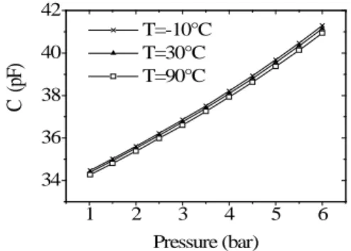
Designed and realized in LAAS, the sensing cell is basically a miniature variable capacitor composed by a silicon diaphragm and a metal plate deposited on a rigid Pyrex 7740 substrate [5]. Silicon and Pyrex are bonded by means of anodic bonding [6]. This type of cells can be electrically modeled by a pure capacitor at medium frequencies (5 to 500 kHz) because of its negligible conductance (≈ 10 nS) and access resistances (few ohms). It presents a high pressure sensitivity, an excellent long term stability and can withstand elevated overpressures [7]. The specimen used to implement the sensor demonstrator has a capacitance in the order of 34 picofarad at rest. The absolute pressure response C for pressures P between 1 and 6 bars and for temperatures θ varying from -10°C to 90°C is shown in Fig. 1. Clearly, the behavior in this operating range is almost linear and can be modeled by :
C(P,θ) = Co(θ) + S(θ) P + NL(P,θ) (1)
where Co is the sensor capacitance when P=0, which is
referred to as the offset capacitance hereafter ; S is the sensitivity parameter depending on the diaphragm structure and its geometry (+ 1.35 pF/bar in this case) ; and NL is the nonlinearity : with respect to a linear model computed using the least squares curve fitting, the nonlinearity, expressed in percentage of the full measurement scale, is in the ± 2.5 % FS range.
1 2 3 4 5 6 34 36 38 40 42 T=-10°C T=30°C T=90°C C ( pF ) Pressure (bar)
Fig. 1 : Absolute response of the sensing cell between
1 and 6 bars and for temperatures from -10°C to 90°C. The thermal behavior of the sensing cell can be evaluated by both the offset and the sensitivity thermal coefficients respectively TC[Co] and TC[S] defined by
TC[X] = ∂X/(X∂θ). As the drifts are quasi-linear between -10°C to 90°C, and very small, these thermal coefficients can be approximated by constants : TC[Co] = - 59 ppm/°C and TC[S] = - 222 ppm/°C.
2.2 Interface circuit
The circuit described in this paper consists of two main blocks : (i) an analog one with two triangular oscillators and (ii) a digital one which gives an 11-bits output number proportional to the capacitance and then to the pressure [8].
(i) Analog block : Capacitance/Period Converter
Several alternative approaches can be used to convert capacitance variations into electrical signal [1],[2],[9],[10]. This converter has been designed to generate a triangular wave-form with time period proportional to the capacitance. It operates on the principle of charge and discharge of a capacitor with constant current I, between two thresholds voltages VL
and VH. This type of oscillator can be modeled by a
charging current source (Io), a discharging one (2Io), a
MOS-T switch and a control logic circuit (CLC) which drives the switching on and the switching off. The CLC consists of two threshold NPN-input comparators and a RS logic-gate.
Considering the switching delay ∆t, the theoretical time period τ of the signal is given by :
τ = τd + kC (2)
where τd ≈ 4 ∆t and k = 2 (VH – VL)/Io.
Even if the CLC has been designed with fastest components, the offset τd remains close to 350 ns.
In order to keep k as constant as possible, threshold voltages are defined by using a high stability reference voltage source (Vref) called "Band-gap source". By
design, the theoretical current value Io is 20.2 µA and
the peak-to-peak amplitude (VH - VL) of the
oscillations is equal to 1.2 V.
Detailed analysis of converter's offset and sensitivity reveal the existence of a leakage current If
and stray capacitors Cs. In the order of 450 nA, If is
essentially due to comparators' input impedance (Zin)
while global stray capacitors have been estimated in the range of 3.5 picofarads. Moreover, in addition to the current source thermal behavior, these two parameters make the converter's thermal drifts much more important (e.g., TC[offset] exceeds 0.2% / °C).
By including If and Cs in (2) and assuming that the
thermal drift of threshold voltages are negligible, the thermal behavior of the converter can be defined by :
(
)
∂ − − ∂ − + − ∂ + + ∂ + − = τ ∂τ in in o o s s Z Z c 1 c 2 I I c 1 c 1 C C b 1 b C C b 1 1 a 1 (3) with a = τd/τ , b = Cs/C and c = (If/Io)2.Even if a, b, c << 1, it clearly appears that the period thermal drifts are still determined by those of the current source.
The easiest improvement to reduce significantly the leakage current consists in replacing the NPN-input comparators by NMOS input comparators.
(ii) Digital block : Ratiometric Digital Output
This block consists of two converters connected to the capacitors C and Cr where C stands for the sensing
cell and Cr for a constant reference capacitor. The main
goal of this block is to generate a binary number proportional to τr/τ (i.e., Cr/C) in order to obtain a
maximum level of self-compensation for both nonlinearities and thermal drifts [11].
While the reference counter counts a constant number No of periods τr, the second one counts N
periods τ such as Nτ = Noτr. Consequently, N is given
by :
N = No τr / τ (4)
Theoretically, if τd << τ, this relationship being
independent of the current. So, its drifts have no impact on the response and then N becomes proportional to Cr/C.
3. SENSOR CHARACTERIZATION
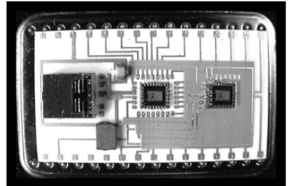
In order to identify primary parameters determining the sensor behavior, two demonstrator versions were implemented and tested. The basic platform is shown in Fig. 2.
Fig. 2 : Evaluation platform composed of integrated
A/D BiCMOS converters, ceramic capacitors and a sensing cell on a ceramic substrate.
3.1 Four chips hybrid sensor
This mock-up results from the assembly of two sensing capacitors and two distinct but similar converters. Pressure is only applied to one of the sensing cells, the other being used as a reference capacitor. As the devices are matched, this implementation offers a high level of self-compensation [11].
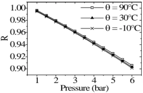
Figure 3 shows the ratio R = N/No between 1 and 6
1 2 3 4 5 6 0.90 0.92 0.94 0.96 0.98 1.00 θ = 90°C θ = 30°C θ = -10°C
R
Pressure (bar)Fig. 3 : Normalized response of the four chips mock-up
Irrespective of temperature, the response is almost linear. The nonlinearity is situated in the range of ± 1.1 % FS. As expected, it is significantly less than that of the sensing cell but not as low as computed in [7]. In addition, the relative sensitivity of this demonstrator is about 1.85% / bar. It is quite two times smaller than that expected.
These results can be explained by stray capacitors Cs connected in parallel to C and Cr. With the simplest
model :
R = (Cr + Cs)/(C + Cs) (5)
Cs has been evaluated in the order of 10 pF. Few
experiences have shown that these stray capacitors are essentially due to interconnections. They introduce a decrease of sensitivity and make the nonlinearity increase [11].
As the offset thermal coefficient doesn't exceed 20 ppm/°C (up to one hundred lesser than that of the converter), the self-compensation of thermal drifts is very efficient.
From (5), the thermal coefficient of the sensor offset is given by (6) : ∂θ ∂ + ∂θ ∂ + − ∂θ ∂ + ∂θ ∂ + = s o s o s r s r o C C C C 1 C C C C 1 ] R [ TC (6)
So, the compensation can be total if the double condition (7) is realized :
Cr = Co and ∂Cr/∂θ = ∂Co/∂θ (7)
3.2 Two chips implementation
This mock-up has been mounted using two converters integrated into the same chip and a silicon/Pyrex sensing cell which contains both the reference and the measurement capacitors. The main goal of such an implementation is to obtain the best possible "matching" of converters, to reduce as much as possible stray capacitors and to assess the feasibility of integration.
Figure 4 represents the comparison between the experimental sensor response and the computed one Cr/C. 1 2 3 4 5 6 0.85 0.90 0.95 1.00 Exp. Theor.
R
Pressure (bar)Fig. 4 : Comparison between experimental and
theoretical response of the two-chip implementation sensor.
It clearly appears that the sensor does not work normally for pressures lower than or equal to 3 bars. That corresponds to a difference of capacitance between C and Cr close to 2.5 pF. For pressure greater
than 3 bars, the "semi-integrated" sensor seems to work correctly. Even if there are some interference, its response is quasi-linear with a relative sensitivity in the range of - 2.5%/°C. This result indicates that stray capacitors have been reduced by two.
4. DISCUSSION
4.1 Phenomena description
Figure 4 shows that the ratio R remains constant and equal to 1 for P ≤ 3 bars. This implies that the two oscillators are working at the same frequency, or in other words, they are synchronized.
Experimentally, the two oscillators output signal have been visualized. It appears that each transition relative to a switch commutation on one oscillator introduce a parasitic voltage pulse on the other.
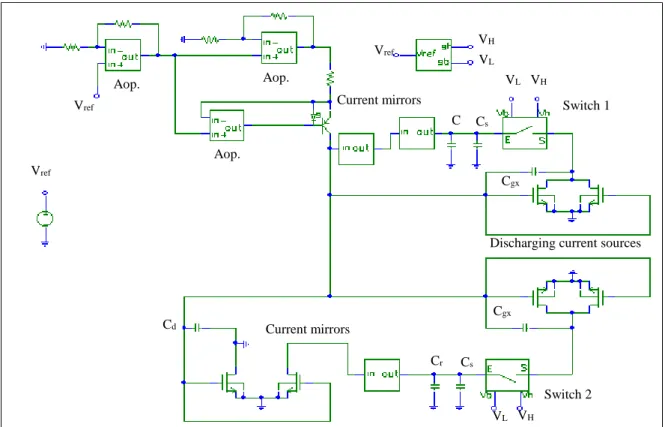
4.2 PSPICE Modeling
The complete sensor behavior has been modeled with PSPICE level 2 as it is shown on Fig. 5. The switch block consists of MOS transistors switch with its CLC.
By design, a switch commutation generates charges injection that provokes a current pulse and then a voltage variation on the triangular wave-form. According to the simple electrical scheme (Fig. 5), it appears that a direct link connects oscillators together through the discharging current sources. Thus, this pulse can be transferred on the other oscillator through MOST grid-to-channel capacitance (Cgx).
Fig. 5 : Simple electric sensor model with PSPICE level 2.
Fig. 6 : Modeling of interference between oscillators
during a commutation.
Figure 6 shows the simulated effect of the reference oscillator switch commutation on the triangular wave-form.
In a first approximation, the magnitude (∆VC) of
these pulses on the triangular signal is directly proportional to the d.c. voltage source (VDD) as it is
described in the relation (8) :
DD ΔV C eq C eq C c ΔV × + ≈ (8)
where Ceq is the equivalent grid-to-channel capacitance
of MOST switch and C is the measured capacitance. With the nominal value VDD = 5 V, the
experimental peak-to-peak magnitude reaches 50 mV. Thus, even if this voltage pulse is strongly reduced on the other triangular wave-form, it still exists.
1 2 3 4 5 6 0.80 0.85 0.90 0.95
R
Pressure (bar)Fig. 7 : Example of a sensor response with C-Cr = 2.5
pF ; visualization of oscillator synchronisation effect. So, for C slightly greater than Cr, the switch
commutation in reference oscillator introduce a pulse which make the other oscillator commute prematurely. It implies that each time commutations happen quasi-simultaneously on both oscillators, it makes the ratio remaining constant. This phenomena is illustrated on Figure 7 that represents the experimental response of the two-chip implementation sensor with C - Cr = 2.5
pF at rest.
4.3 Design optimization
The most efficient method to eliminate the oscillators synchronization is to design two distinct oscillators with their own current source. But, this
Cs Cgx Cs Cd Current mirrors Cr Current mirrors C VL VH VL VH Vref Vref Vref VH VL Aop. Aop. Aop. Switch 2 Discharging current sources
Cgx
method procures two main drawbacks : first, the integrated circuit area will be more important and then makes the sensor more expensive ; secondly, the matching between current sources will be poor due to component dispersion). That implies a worst efficiency of self-compensation (see section 2.2).
From eqn. (8), one solution to minimize pulses magnitude and make them negligible consists in reducing the ratio Ceq/C. Assuming that MOST
capacitances (Cgs and Cgd) are directly proportional to
the channel width W, electrical simulations have shown that an other solution consists in reducing this parameter (i.e. MOST dimensions). But, even if the voltage variation due to switch commutation seems to be proportional to W, the MOST dimensions can't be indefinitely reduced. Effectively, the MOST output conductance increases while form factor decreases. Thus, the discharging current will not be constant and then disrupts sensor operation.
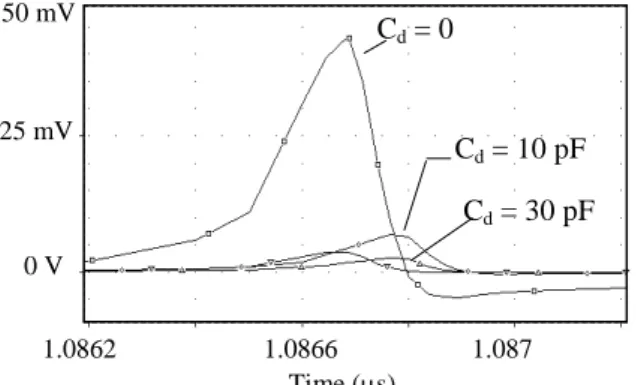
So, an other way to minimize this coupling effects is to add a decoupling capacitance Cd between current
mirror grids and ground. PSPICE simulations, shown in Fig. 8, indicate the attenuation efficiency of Cd on the
transmitted pulse magnitude.
10 mV 5 mV 0 V Temps (µs) Signal de commande (v(t)) Cd = 0 Cd = 30 pF Cd = 10 pF Time (µs) 1.0862 1.0866 1.087 0 V 25 mV 50 mV
Fig. 8 : Simulation of pulse attenuation efficiency of a
decoupling capacitance.
5. CONCLUSION
The pressure sensor described here is an hybrid association of a capacitive sensing cell in Silicium/Pyrex technology, and a capacitance-to-frequency transducer based on the charge and the discharge of a capacitor with constant current. The modeling response of each part allows us to explicit the transfer function of the sensor. Accurate evaluation of different parameters is achieved by both numerical simulation and experimental characterisation of the sensing cell and the electronic circuit. Studies on a simple and a ratiometric architecture show the feasibility of pressure sensor which is able to mainly self-compensate nonlinearity and drifts. In the range of ten percent of the offset frequency, the demonstrator nonlinearity is less than one percent and its thermal coefficient is about twenty parts of million by Celsius degree. Numerical simulations show that to optimize ratiometric sensor performances, it is necessary to use a
perfect symmetrical architecture. These optimal performances can be obtained by integrating both converters on the same silicon substrate. Experimental results also point out several problems of interference between oscillators through grid-to-channel capacitances. One way to minimize these coupling effects is to add a 30 pF decoupling capacitance at least.
All the results obtained allow us to conclude that measurement principles and the associated technologies used are adequate to develop a new family of miniature pressure sensor which can be relatively accurate (about 1% of the full scale), cheap and easily connected with numerical communication networks.
6. REFERENCES
[1] Mitsuhiro Yamada, Member, IEEE, and Kenzo Watanabe, Fellow, IEEE, "A Capacitive Pressure Sensor Interface Using Oversampling ∆-Σ Demodulation Techniques", IEEE Transactions on Instrumentation and Measurement, Vol. 46, No. 1, pp 3-7, Feb. 1997.
[2] H. Matsumoto, H. Shimizu and K. Watanabe, "A Switched Capacitor Charge Balancing analog-to-digital converter and its application to capacitance measurement", IEEE Tans. Instrum. Meas., vol. IM-36, pp. 873-878, dec. 1987.
[3] C. A. Leme, P. Malcovati and H. Baltes, "Oversampled interface for IC sensors", in Proc. Instrumentation and Measurement Tech. Conf., 1994, pp. 652-655.
[4] P. Pons and G. Blasquez, "Low-cost high sensitivity integrated pressure and temperature sensor", Sensors & Actuators A, vol. 41-42 (1994) pp. 398-401.
[5] G. Blasquez, Y. Naciri, P. Blondel, N. Benmoussa and P. Pons, "Micromachined Silicon Capacitive Sensor", Proc. 2nd Int. Conf. Passive Comp. Mat. Tech. Processing, Paris 18-20 nov. 1987, pp. 142-146. [6] T. Rogers and J. Kowal, "Selection of Glass : Anodic
bonding conditions and material compatibility for silicon-glass capacitive pressure sensors", Sensors & Actuators A, Vol. 46-47, (1995) pp. 113-120.
[7] P. Pons, G. Blasquez, R. Behocaray, "Feasability of Capacitive Pressure Sensor Without Compensation Circuits", Sensors & Actuators A, 37-38 (1993), pp. 112-115.
[8] Ph. Dondon, Ch. Zardini and J. L. Aucouturier, "BiCMOS integrated circuit for capacitive pressure sensors in automotive applications", Sensors & Actuators A, 37-38 (1993), pp. 596-599.
[9] D.R. Harrison and J. Dimeff, "A diode-quad bridge for use with capacitive transducers", Rev. Sci. Instrum., vol. 44, p. 1468, Oct. 1973.
[10] G. Blasquez, P. Pons, Ph. Menini, D. Herbst, M. Schulz, and B. Höfflinger, "Capacitive pressure mock-up without compensation circuits", Transducers'95 - Eurosensors IX, June 1995, Stockholm, Sweden, pp. 628-631.
[11] G. Blasquez, P. Pons, Ph. Menini, X. Chauffleur, Ph. Dondon and C. Zardini, "Efficiency of a BiCMOS ratiometric circuit to self-compensate for nonlinearities and thermal drifts in capacitive pressure sensors", 10th European Conference on Solid State Transducers (Eurosensors X), Leuven, Belgium, 8-11 sept. 1996, pp. 359-362.