O
pen
A
rchive
T
OULOUSE
A
rchive
O
uverte (
OATAO
)
OATAO is an open access repository that collects the work of Toulouse researchers and
makes it freely available over the web where possible.
This is an author-deposited version published in :
http://oatao.univ-toulouse.fr/
Eprints ID : 13581
To link to this article :
DOI:10.1002/sia.5389
URL :
http://dx.doi.org/10.1002/sia.5389
To cite this version :
Beche, Eric and Balat-Pichelin, Marianne and Flaud, Valérie and
Esvan, Jérôme and Duguet, Thomas and Sciti, Diletta and Alfano,
Davide XPS and AES studies of UHTC ZrB2-SiC-Si3N4 treated with
solar energy. (2014) Surface and Interface Analysis, vol. 46 (n°
10-11). pp. 817-822. ISSN 0142-2421
Any correspondance concerning this service should be sent to the repository
XPS and AES studies of UHTC ZrB
2
–SiC–Si
3
N
4
treated with solar energy
†
E. Beche,
a* M. Balat-Pichelin,
bV. Flaud,
cJ. Esvan,
dT. Duguet,
dD. Sciti
eand D. Alfano
fThe microstructure of ultra-high-temperature ceramics based on the ZrB2–SiC composition and a sintering additive (Si3N4) was
investigated using XPS and AES techniques. These ZrB2–SiC–Si3N4materials were treated in air plasma at high temperature
(T > 1750 K) in the MESOX facility developed at the PROMES-CNRS laboratory (Moyen d’Essai Solaire d’OXydation for the measurement of atomic oxygen recombination coefficients). The surfaces were characterized before and after the air plasma treatment. Surface modifications were observed and induced by the oxidation process. The elementary composition was determined using AES and XPS. Core level spectroscopy (XPS) was used to determine the atomic composition and the nature of the chemical bonds from the Zr 3d3/2,5/2, Si 2p1/2,3/2, O 1s and C 1s photoelectron peaks. The microstructural analyses
revealed the presence of oxide layers: Silica and zirconia compounds were detected at temperatures near 1800 K, and a zirconia compound was mainly detected above 2200 K.
Keywords: XPS; AES; ultra-high-temperature ceramics; zirconium diboride; silicon carbide
Introduction
A ground test simulation in atmospheric re-entry conditions is neces-sary to characterize and select base materials for a thermal protection system (TPS). The thermophysical and microstructural properties are key parameters for the eligibility of ultra-high-temperature ceramic (UHTC) materials in hot structure manufacturing.
The base materials for future spaceplane-like, re-entry vehicles must resist temperatures approaching 2500 K and evaporation, erosion and oxidation in the harsh re-entry environment. These requirements are above the single-use temperature limit of current TPS materials (SiC-coated C–C composites).[1,2]
Ceramic compounds based on metal borides, such as zirconium diboride (ZrB2) and hafnium diboride (HfB2), are defined as UHTCs
because of their high melting temperatures, which are greater than 3300 K.[3,4]ZrB2materials have a lower theoretical density (6.09 g/
cm3), which classifies them as the most promising candidates for TPSs. The presence of SiCfibers increases the mechanical proper-ties (matrix stability) of the ZrB2–SiC material. The value of the
fracture toughness in ZrB2ceramics is approximately 3.8 MPa.m1/2
and increases to approximately 5.3 MPa.m1/2in ZrB2ceramic + SiC
fibers. Several authors[5–8]have demonstrated that the
incorpora-tion of SiC provides significant enhancements to the oxidation resistance; a small amount of the formed borosilicate compound limits the oxygen diffusion. The incorporation of Si3N4 in the
ZrB2matrix improves the sintering temperatures; the sintering
temperature decreases from 2090 K (30 MPa, 20 min) to 1950 K (30 MPa, 10 min). During an oxidation process in air (T = 1500 K) of a ZrB2–SiC composite, several authors[9]reported that the thickness
of the oxide layer decreases with an increasing amount of SiC from 0% to 50% (vol.) in the reference material.
Understanding the chemical environment of the surface and in the bulk is necessary to explain the surface properties and the phe-nomena regulating the surface oxidation of these UHTC materials. These materials are considered an attractive class of TPS ceramic
compounds for aerospace applications such as sharp leading edges and the hot structures of slender-shaped re-entry vehicles.
ZrB2UHTCs are processed using hot pressing. Complex-shaped
components can then be obtained using either conventional diamond machining or electrical discharge machining (EDM), which is possible because of the electrical conductivity of the borides (106S/cm). The surface finish can be better controlled using conventional machining. However, EDM is effective and can be used to machine UHTC pieces into complex-shaped components such as nose-cones or sharp leading edges.[7]
In the last decade, the oxidation of ZrB2–SiC UHTC materials
(near 2000 K) using an XPS technique was studied in less than ten publications. No surface study using AES for oxidized ZrB2–SiC UHTC materials was performed. The initial oxidation
of ZrB2 surfaces at high temperature (1600 K) was characterized
by Aizawa et al.[10]The authors present the AES spectra (Zr MNN, B KLL and O KLL) of a clean ZrB2and an exposed ZrB2surface under
O2gas at 1600 K. Rayner et al. [11]
studied the evolution of the Zr
* Correspondence to: E. Beche, CNRS-PROMES, SASI, 7 rue du Four Solaire, Font Romeu 66120, France.
E-mail: eric.beche@promes.cnrs.fr
† Paper published as part of the ECASIA 2013 special issue.
a PROMES-CNRS-SASI, 7 rue du Four Solaire, 66120 Font Romeu, France b PROMES-CNRS, MHTCS, 7 rue du Four Solaire, 66120 Font Romeu, France c ICGM-CNRS, Place Eugène Bataillon, 34095 Montpellier Cedex 5, France d CIRIMAT-ENSIACET, 31030 Toulouse Cedex 4, France
e ISTEC-CNR, Via Granarolo, 48018 Faenza, Italy f CIRA, Via Majorise, 81043 Capua, Italy
MVV, Si LVV and O KVV transitions by AES for as-deposited (ZrO2)x
(SiO2)1 xalloys.
The aim of this work is to investigate the microstructure of reference and treated UHTC materials based on the ZrB2–SiC
composition with a sintering additive (Si3N4) using XPS and
AES. Qualitative and quantitative analysis was conducted using core level spectroscopy (XPS).
Experimental section
Ceramic compounds were prepared using the following commer-cial powders: SiC choppedfibers (HI Nicalon, COI Ceramics Inc., Magna, Utah, USA) and ZrB2Grade B (H.C. Starck, Germany). For
the sintering aids, Si3N4 Baysind (Bayer, Germany) were used.
The following composition of sample A was produced (vol%): ZrB2+ 15% SiC + 5% Si3N4.
The UHTC compounds were obtained by hot pressing of powders and SiCfibers.[7]The powders andfiber mixtures were
ball milled for 24 h. After solvent removal, the powder mixture was uniaxially pressed at 15 MPa to form 45-mm diameter green pellets. Before sintering, the pellets underwent a debonding cycle at 773 K to remove organic species. The pellets were subse-quently hot pressed using a load of 40–50 MPa. Because the reinforcingfibers tend to react with the matrix and secondary phases during the high-temperature thermal treatment, the sintering temperature should be kept as low as possible.
The UHTC materials were heated in a MESOX solar reactor (6 kW). This apparatus is described in detail in previous papers.[7,12,13] Concentrated solar energy was used to heat the sample placed at the center of the microwave discharge (300 W); i.e. the air plasma conditions were kept constant, and only solar heating was transformed to increase the sample temperature for the measurement of the recombination coef fi-cient.[12]The degree of oxygen dissociation was high (70–80%).
The heating of the samples was independent from the plasma. The heating began at 1000 K and increased every 10 min by a step of 200 K until reaching thefinal temperatures (T = 1760 K, sample A1, and T = 2200 K, sample A2) for 1 h. Control of the tem-peratures was possible with an opening shutter. The temperature measurement was performed using a monochromatic (5μm) optical pyrometer considering the normal spectral emissivity. Moreover, the pyrometer, the CaF2window and the mirror were
calibrated in our laboratory on a blackbody.
AES analysis was performed using a Thermoelectron MICROLAB 350 device (CIRIMAT-ENSIACET, France). The Auger electron emission spectra were recorded using electron gun (5 kV). The analyzed area was ~1μm2. The spectrometer energy calibration was made using the Si KL2,3L2,3(1615.8 ± 0.1 eV) and
the Si L2,3VV (92.9 ± 0.1 eV) Auger transition from a Si(100) wafer
sam-ple. AES spectra were recorded in direct N(E). The kinetic energy (KE) scale was established by referencing the C KVV value of adventitious carbon (267.8 eV). The ionic sputtering of the surfaces was made by Ar + ion beam accelerated under 3 keV, 1.5μA for 60 s.
XPS analysis was performed using a Thermoelectron ESCALAB 250 device (ICGM, France). The photoelectron emission spectra were recorded using Al–Kα radiation (hν = 1486.6 eV) from a monochromatized source. The analyzed area was ~0.15 mm2. The pass energy was fixed at 20 eV. The spectrometer energy calibration was made using the Au 4f7/2(83.9 ± 0.1 eV) and Cu
2p3/2 (932.8 ± 0.1 eV) photoelectron lines. XPS spectra were
recorded in direct N(Ec). The background signal was removed
using the Shirley method.[14] The atomic concentrations were
determined with an accuracy of 10% from photoelectron peak areas using the atomic sensitivity factors reported by Scofield,[15]
taking into account the transmission function of the analyzer. This function was calculated at different pass energies from Ag 3d and Ag MNN peaks collected for a silver reference sample. The binding energy scale was established by referencing the C 1s value of adventitious carbon (284.8 eV).[16]The photoelectron peaks were analyzed by Gaussian/Lorentzian (G/L = 50) peakfitting.
According to our studies on material surface degradation by ions, the ionic sputtering of thefilms surfaces was made by Ar + ion beam accelerated under 2 keV. The ion flux was fixed at about 15μA/cm2for 30 s.
Thefixed full width at half maximum and the fixed positions of the components were similar to those collected for several reference samples: zirconium (IV) oxide, Sigma Aldrich (Missouri, US), 99.99%; zirconium (IV) oxide, Neyco (Paris, France), sputtering target 99.5%; zirconium diboride, Neyco, sputtering target 99.5%; andβ-SiC, PI-Kem Ltd. (Staffordshire, UK), 99.9%.
Results and discussion
The atomic compositions of the sputtered samples A, A1 and A2 were measured based on the O 1s, Zr 3d, B 1s, Si 2p, C 1s and N 1s core level photoelectrons peaks (Table 1). For sample A, the presence of residual oxide layers (sample A) and carbon species is explained by the finishing treatment; the electric discharge machining (EDM) leads to the presence of zirconia, silica and a high amount of carbon on the sample.
The assignment of the O 1s, Zr 3d, B 1s, Si 2p, C 1s and N 1s components from the XPS spectra collected for the UHTC com-pounds A, A1 and A2 is summarized in Table 2. For the heated samples A1 and A2, the atmospheric contamination components (C–C/C–H and/or C–O bonds) of the C 1s photoelectron peaks are not shown in Table 2.
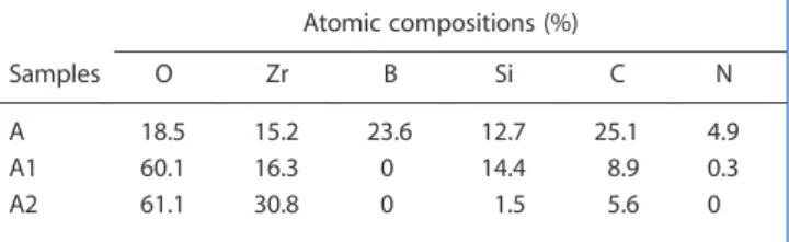
The Zr 3d spectra collected for sample A (Fig. 1a) and samples A1 and A2 (Figs 1b and 1c) havefive or two components, respectively. The ratio of the peak intensities, R = (I 3d5/2/I 3d3/2), wasfixed to
1.50 ± 0.05. The spin–orbit energy difference between the 3d5/2
and the 3d3/2components is approximately 2.38 ± 0.02 eV. The Zr
3d5/2and Zr 3d3/2peak positions located at 179.2, 181.6 ± 0.1 eV
are attributed to the Zr–B bonds in a ZrB2compound.[7,8,10,17]
The Zr 3d5/2and Zr 3d3/2peak positions located at
approxi-mately 182.6 and 185.1 ± 0.1 eV are characteristic of the O–Zr bonds in oxide compounds.[7,8,17,18]The Zr atoms are in Zr–O4
environments (Zr4+state). For the treated samples A1 and A2, no Zr–B components were detected.
The B 1s spectrum (Fig. 1a, sample A) located at 187.8 ± 0.1 eV was attributed to B–Zr bonds (ZrB2 compound).
[7,8,10,17]
No B element was detected for the tested samples A1 and A2.
Table 1. Atomic compositions (%) measured from the O 1s, Zr 3d, B 1s, Si 2p, C 1s and N 1s spectra Atomic compositions (%) Samples O Zr B Si C N A 18.5 15.2 23.6 12.7 25.1 4.9 A1 60.1 16.3 0 14.4 8.9 0.3 A2 61.1 30.8 0 1.5 5.6 0
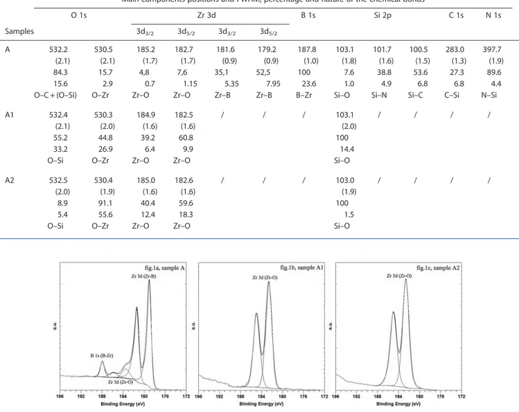
The three components (103.1, 101.7 and 100.5 ± 0.1 eV) of the Si 2p spectrum (sample A, Fig. 2a) were attributed to Si–O, Si–N and Si–C bonds, respectively.[10,19–21]No Si–N and Si–C bonds were detected on the surfaces of samples A1 and A2 (Figs 2b and 2c).
The O 1s spectra (Figs 3a–c) were curve fitted with two compo-nents. The component located at 530.4 ± 0.1 eV is attributed to O–Zr bonds.[7–17]These bonds are larger for sample A2 than those for sample A1. The shift between the O–Si and O–C component is less than 0.3 eV. Thus, in the peak-fitting process, only one compo-nent (532.4 ± 0.1 eV) was used to identify these two types of bonds (O–C and O–Si).[10,19]For samples A1 and A2 (Figs 3b and 3c), this
component is mainly attributed to O–Si bonds (Table 2). However, for sample A (Fig. 3a), this component is mainly attributed to O–C bonds (Table 2).
The C–Si bonds (283.0 ± 0.1 eV)[4,5,9–11]were only detected on surface A (not shown).
The N 1s spectrum (A) was mainly curvefitted with one compo-nent (not shown). The main compocompo-nent located at 397.6 ± 0.1 eV was attributed to N–Si bonds[20](Si
3N4 compound). N–Si bonds
were only detected from the N 1s photoelectron peaks of sample A.
For sample A, the residual oxide layers and carbon species were not completely removed during the sputtering process. An induced surface roughness is revealed in SEM micrographs. The XPS results reveal the microstructure of a ZrB2–SiC–Si3N4
compound.
For samples A1 and A2, the ZrB2,the SiC and the Si3N4phases
detected on the reference surface A were fully oxidized. These results indicate that two oxide phases, SiO2and ZrO2, were formed
in the heated initial surface. Higher temperatures were correlated with lower amounts of SiO2 and higher amounts of ZrO2: When
the temperature increased to 1760 K, silica was embedded in zirco-nia for the same heating time. The presence of Zr–O–Si bonds in ZrSiOxinduced shifts of the Si 2p, Zr 3d and O 1s spectra: The
com-ponents attributed to mixed Zr–O–Si bonds in ZrSiO4compounds
are detected at 101.8, 183 and 531.3 eV, respectively.[11]No (ZrO 2) x(SiO2)1 xmixed alloys with Zr–O–Si bonds were observed from
the Zr 3d, Si 2p and O 1s spectra.
Several points of a line scan (AES) were taken on the clean sur-face of sample A. Two types offield, pt1 and pt2, were identified (Fig. 4b).
Figure 1. Zr 3d XPS spectra collected for samples A, A1 and A2.
Table 2. Main components positions (±0.1 eV), FWHM (±0.05 eV), percentage of each chemical bonds in the photoelectron peaks (O 1s, Zr 3d, B 1s Si 2p, C 1s and N 1s), percentage of the chemical bonds related to the atomic compositions of each element (O, Zr B, Si, C and N): samples A, A1 and A2
Main components positions and FWHM, percentage and nature of the chemical bonds
O 1s Zr 3d B 1s Si 2p C 1s N 1s Samples 3d3/2 3d5/2 3d3/2 3d5/2 A 532.2 530.5 185.2 182.7 181.6 179.2 187.8 103.1 101.7 100.5 283.0 397.7 (2.1) (2.1) (1.7) (1.7) (0.9) (0.9) (1.0) (1.8) (1.6) (1.5) (1.3) (1.9) 84.3 15.7 4,8 7,6 35,1 52,5 100 7.6 38.8 53.6 27.3 89.6 15.6 2.9 0.7 1.15 5.35 7.95 23.6 1.0 4.9 6.8 6.8 4.4 O–C + (O–Si) O–Zr Zr–O Zr–O Zr–B Zr–B B–Zr Si–O Si–N Si–C C–Si N–Si
A1 532.4 530.3 184.9 182.5 / / / 103.1 / / / /
(2.1) (2.0) (1.6) (1.6) (2.0)
55.2 44.8 39.2 60.8 100
33.2 26.9 6.4 9.9 14.4
O–Si O–Zr Zr–O Zr–O Si–O
A2 532.5 530.4 185.0 182.6 / / / 103.0 / / / /
(2.0) (1.9) (1.6) (1.6) (1.9)
8.9 91.1 40.4 59.6 100
5.4 55.6 12.4 18.3 1.5
The main Auger transitions, Zr M4,5N1N2,3, Zr M4,5N2,3N2,3and
Zr M4,5N2,3N4,5 (pt1, Fig. 4a), are located at 92.7, 117.7 and
147.5 ± 0.2 eV. The peak at 176.7 ± 0.2 eV is mainly assigned to the B KL2,3L2,3 transition (pt1, Fig. 4a) and a weak overlap of a
Zr Auger transition (low kinetic energy (KE) side).
The Si L2,3VV and C KVV Auger transitions (pt2, Fig. 4a) are
located at 86.5 and 266.0 ± 0.2 eV, respectively. These positions are characteristic of a SiC compound. Weak Zr MNN and B KL2,3L2,3Auger transitions were also observed.
The spectra pt1 and pt2 (sample A) are characteristic of a ZrB2
ceramic and SiCfiber, respectively.
Several points of a line scan (AES) were taken on the clean surface of samples A2 and A1. For sample A2, one characteristic point, pt3, was identified (Fig. 5b). For sample A1, two characteristic points, pt4 and pt5, were identified (Fig. 5c).
Figure 5a presents the AES spectra collected from the clean surfaces of samples A2 and A1. The spectra (A2, pt3) and (A1, pt4) were collected on the oxidized ZrB2ceramic. The spectra (A1, pt5)
were collected on an oxidized SiCfiber.
The position of the Zr MNN Auger transitions were all shifted to the low KE side ( 5 eV) in comparison with the KE positions mea-sured for sample A (pt1, Fig. 4). This result indicates the presence
Figure 2. Si 2p XPS spectra collected for samples A, A1 and A2.
Figure 3. O 1s XPS spectra collected for samples A, A1 and A2.
of a ZrO2compound. [22,23]
The peak (77.4 ± 0.2 eV), which is only detected for sample (A1, pt5), is attributed to the Si L2,3VV transition
in SiO2compounds. [22,24]
The ZrB2–SiC–Si3N4compounds of samples A1 and A2 are fully
oxidized. Silica and zirconia are detected for sample A1, but zirconia is only detected for sample A2.
For sample A1, the oxidized SiCfibers located at the surface are partially covered by zirconia, which diffuses during the heat treat-ment. The oxidized SiCfibers (silica compound) are embedded in a zirconia layer.
No oxidized SiCfiber was observed on the surface of sample A2. The holes and valleys correspond to the initial position of the SiC fibers, which were burnt during the heat treatment (T = 2200 K).
Conclusions
XPS and AES analyses revealed significant results for the tested surfaces at various temperatures. For the non-tested sample, the surface layer was characteristic of SiC fibers embedded in ZrB2matrix.
The tested ZrB2–SiC–Si3N4 materials were fully oxidized at
1760 and 2200 K. Higher temperatures were correlated with lower amounts of silica. At 1760 K, the surface layer was composed of a matrix of zirconia and oxidized fibers (silica compound). When the temperature increased to 2200 K, all the SiC fibers were burnt. The surface layer is a zirconia compound that contains holes and valleys corresponding to the initial SiC fibers.
This study highlights the extreme complexity of UHTC oxida-tion behavior. Knowledge about the chemical environment on the surface and in the bulk is necessary to explain the surface properties and phenomena regulating the surface oxidation of these UHTC materials.
Acknowledgements
This work has been funded by the Seventh Framework Program of the European Union (SFERA grant agreement no. 228296).
References
[1] T. Laux, T. Ullmann, M. Auweter-Kurtz, H. Hald, A. Kurz. Proceeding of the 2ndInternational Symposium on Atmospheric Re-entry Vehicles and Systems. 2001, 1.
[2] A. Mühlratzer, M. Leuchs. Applications of non-oxide CMCs. In Pro-ceedings of the 4th International Conference on High Temperature Ceramic Matrix Composites. 2001, 288.
[3] W. G. Fahrenholtz, G. E. Hilmas, I. G. Talmy, J. A. Zaykoski, J. Am. Ceram. Soc. 2007, 90, 1347.
[4] C. Mroz, Am. Ceram. Soc. Bull. 1994, 73, 141.
[5] L. Kaufman, E. V. Clougherty, Investigation of Boride Compounds for Very High Temperatures Application, Manlabs Inc, RTD-TRD-N63-4096, Pt. III, Cambridge, MA, 1966.
[6] L. Scatteia, R. Borrelli, G. Cosentino, E. Beche, J. L. Sans, M. Balat-Pichelin, J. Spacecraft Rockets, 2006, 43, 1004.
[7] D. Alfano, L. Scatteia, F. Monteverde, E. Beche, M. Balat-Pichelin J. Eur. Ceram. Soc. 2010, 30, 2345.
[8] D. Gao, Y. Zhang, J. Fu, C. Xu, Y. Song, X. Shi, Corros. Sci. 2010, 52, 3297.
[9] P. Sarin, P. E. Driemeyer, R. P. Haggerty, D. K. Kim, J. L. Bell, Z. D. Apostolov, J. Eur. Ceram. Soc. 2010, 30, 2375.
[10] T. Aizawa, S. Hishita, S. Otani, Appl. Surf. Sci. 2009, 256, 1120. [11] G. B. Rayner, D. Kang, Y. Zhang, G. Lucovsky, J. Vac. Sci. Technol. B
2002, 20, 1748.
[12] M. Balat-Pichelin, J. M. Badie, R. Berjoan, P. Boubert, Chem. Phys. 2003, 291, 181.
[13] M. Balat, M. Czerniak, J. M. Badie, Appl. Surf. Sci. 1997, 120, 225. [14] D. A. Shirley, Phys. Rew. B, 1972, 5, 4709.
[15] J. H. Scofield, J. Electron Spectrosc. Relat. Phenom., 1976, 8, 129. [16] M. P. Seah, Practical Surface Analysis (2nd edn), vol. 1, (Eds: D. Briggs,
M. P. Seah), J. Wiley & Sons, New York, 1993, 543. Figure 5. (a) AES spectra collected for samples A1 and A2, (b) SEM
micrograph of the surface (sample A2) and (c) SEM micrograph of the sur-face (sample A1).
[17] C. Monticelli, F. Zucchi, A. Pagnoni, M. Dal Colle, Electrochim. Acta, 2005, 50, 3461.
[18] E. Beche, G. Peraudeau, V. Flaud, D. Perarnau, Surf. Interface Anal., 2012, 44, 1045.
[19] S. Scordo, M. Ducarroir, E. Bêche, R. Berjoan, J. Mater. Res. 1998, 13, 3315. [20] N. Nakamura, K. Hirao, Y. Yamauchi, Nucl. Intrum. Meth. Phys. Res. B,
2004, 217, 51.
[21] J. Eck, M. Balat-Pichelin, L. Charpentier, E. Bêche, F. Audubert, J. Eur. Ceram. Soc., 2008, 28, 2995.
[22] L. M. Eshelman, A. M. de Jong, J. W. Niemantsverdriet, Catal. Lett., 1991, 10, 201.
[23] Y. Baba, T. A. Susaki, Surf. Interface Anal., 1984, 6, 171.
[24] A. Glachant, P. Soukiassian, P. S. Mangat, J. Peng, S. T. Kim, Appl. Surf. Sci. 1992, 56, 802.