HAL Id: hal-01940661
https://hal.archives-ouvertes.fr/hal-01940661
Submitted on 17 Jul 2019
HAL is a multi-disciplinary open access
archive for the deposit and dissemination of
sci-entific research documents, whether they are
pub-lished or not. The documents may come from
teaching and research institutions in France or
abroad, or from public or private research centers.
L’archive ouverte pluridisciplinaire HAL, est
destinée au dépôt et à la diffusion de documents
scientifiques de niveau recherche, publiés ou non,
émanant des établissements d’enseignement et de
recherche français ou étrangers, des laboratoires
publics ou privés.
A Novel Configuration of a Microstrip Microwave
Wideband Power Amplifier for Wireless Application
Amine Rachakh, Larbi El Abdellaoui, Jamal Zbitou, Ahmed Errkik, Abdelali
Tajmouati, Mohamed Latrach
To cite this version:
Amine Rachakh, Larbi El Abdellaoui, Jamal Zbitou, Ahmed Errkik, Abdelali Tajmouati, et al.. A
Novel Configuration of a Microstrip Microwave Wideband Power Amplifier for Wireless
Applica-tion. Telkomnika (Telecommunication, Computing, Electronics and Control), Institute of Advanced
Engineering and Science (IAES), 2018, 16 (1), pp.224-231. �10.12928/telkomnika.v16i1.7369�.
�hal-01940661�
DOI:10.12928/TELKOMNIKA.v16i1.7369 224
A Novel Configuration of a Microstrip Microwave
Wideband Power Amplifier for Wireless Application
Amine Rachakh*1, El Abdellaoui Larbi2, Zbitou Jamal3, Ahmed Errkik4, Abdelali Tajmouati5, Latrach Mohamed6
1, 2,3,4,5
LMEET, FST of Settat Hassan 1st University Settat, Morocco. University Complex, Casablanca Road, Km 3.5, B.P: 577 Settat, Morocco. 6
Microwave group ESEO Angers France, 10 Bd Jeanneteau - CS 90717 49107 ANGERS CEDEX 2. *Corresponding author, e-mail: rachakh.amine1@gmail.com
Abstract
RF/microwave power amplifier (PA) is one of the components that has a large effect on the overall performance of communication system especially in transmitter system and their design is decided by the parameters of transistor selected. This letter presents a new concept of a wide-band microwave amplifier using scattering parameters that is often used in the radio frequency communication systemas an application of the active integrated antenna[1- 2]. This power amplifier operates from 1.75 GHz to 2.15GHz frequency and it is based on AT-41410 NPN transistor that has a high transition frequency of 10GHz. The proposed Single Stage PA is designed by microstrip technology and simulated with Advanced Design System (ADS) software. The simulation results indicate good performances; the small power gain (S21) is changed between 11.8 and 10dB. For the input reflection coefficient (S11) is varied between 11 and -22.5dB. Regarding the output reflection coefficient (S22) is varied between -13.1 and -18.7dB over the wide frequency band of 1.75-2.15GHz and stability without oscillating over a wide range of frequencies.
Keywords: wideband power amplifier, microstrip technology, input matching, output matching, bipolar
junction transistors (BJTs), advanced design system (ADS)
Copyright © 2018 Universitas Ahmad Dahlan. All rights reserved.
1. Introduction
As wireless communication technology advances, Microwave power amplifier becomes an important study issue, because it is the key component of wireless communication transmitter [3]. Communication quality and power consumption of the communication device depend on performance of the amplifier. Although power amplifiers are parts of the transmitters only, their design should take into consideration the general features of the full communications system [4]. One of the key design goals for the power amplifier is a good impedance matching, together with a wide bandwidth, a sufficiently large power gain range and a low power consumption.
The wideband and the narrow band microwaves power amplifiers are very utilized in the detection and the communication systems (radio communication, spatial telecommunication, control system, radar detection …) [5]. The matching networks of these power amplifiers are designed through distributed elements (transmission lines) or to basis of localized elements (capacitors and inductances) orassociation of both techniques [6,12]. The employ of the matching networks by the distributed elements or localized elements depend on the operation frequency. Indeed, for low frequencies the localized elements are mostly used, and for the more high frequencies the distributed elements are widely used, this for technological constraints and the economic [9].
In this work, we present a new design of a wide-band microwave power amplifier using the transistor AT-41410 that of type Si-BJT (Bipolar Junction Transistor). This power amplifier utilizes microstrip transmission lines matching to match the input and output at 50 Ohm. In what follows, we present the design of a wide-band microwave power amplifier using s-parameters, where we study the microwave amplifier in the DC mode and next we simulate the amplifier using ADS (Advanced Design System) software. In addition, we show the performances of the microwave wide-band amplifier. Finally, we conclude.
TELKOMNIKA ISSN: 1693-6930
A Novel Configuration of a Microstrip Microwave Wideband Power Amplifier for… (A Rachakh) 225 2. Design of a Wide-Band Microwave Power Amplifier Using S-Parameters
The block diagram of the microwave PA is presented in Figure 1. The impedance matching network at the base and collector terminals of the BJT transistor is designed to match the wide bandwidth signal with a 50 Ω system impedance. The bias network used to determine the PA performance over tension as well as RF drive.
Figure 1. Basic microwave power amplifier schematic
In order to obtain good performancesfor a microwave power amplifier, the input and the output impedances of the device must be matched. Among various types of matching networks (MN) we can find:
a. Quarter-wave transformers. b. Multi-section transformers. c. Lumped Elements.
d. Microstrip line & single (or double) stub.
Microstrip amplifier are widely used for wireless applications as: military purposes, satellite communication, GPS, missile systems, mobile etc. This kind of microwave amplifier presents some advantages:
a. It has a very low fabrication cost. b. Ease of manufacturing.
c. Easy in integration with microwave passive and active circuits.
According to idea noticed above as illustrated in Figure 1 we propose a wide-band microwave PA with a microstrip technology and by using scattering parameters. This PA works from 1.75 GHz to 2.15GHz frequency, we can increase or decrease the frequency band by adding or removing the number of stubs in the input or the output side. Figure 2 gives the proposed schematic of the overall microstrip microwave power amplifier.
Figure 2(a). Input matching network circuit Figure 2(b). Output matching network circuit
Figure 2(c). Biasing circuit
The designs of PA, there are various common aims. These contain reducing the reflections of the PA, producing large power gain with high output power and assuring stable condition. Are all-important considerations [13]. In order to make a PA, the selection of active device is critical. This is one of the most influential steps in designing a PA. Different types of active devices are used for power amplifier applications. In accordance with specifications, adequate transistor should be chosen for PA owing to its high gain and low cost [14]. The numbers of transistors are finite at the frequency of applications. In this work, AT-41410 is chosen.
3. DC-mode of Microwave Amplifier
To study the functioning of AT-41410 microwave transistor in DC mode, we raised the characteristics network IC=f (VCE,IB) through the ADS software. Figure 3 shows this characteristic network of AT-41410. For biasing the transistor in the linear zone of its characteristic, we adopted the DC equivalent schematic of microwave power amplifier that is shown in the Figure 4. We determine the resistances of biasing R1, R2, R3 and R4 allowing to
TELKOMNIKA ISSN: 1693-6930
A Novel Configuration of a Microstrip Microwave Wideband Power Amplifier for… (A Rachakh) 227
Figure 3. The Characteristics Network IC=f
(VCE, IB) of Transistor AT-41410
Figure 4. DC Equivalent Schematic of Microwave Power Amplifier
In order to determine the values of the biasing resistances, we should have four equations; two equations are given from Kirchhoff's loop rule, whilst the two others from the two following conditions: IB1=9 IB and we want a voltage fall to boundary-marks of R5 equals to 3V.
From the Figure 4, the resistance R1 can be calculated as:
3 1 2 CE BE C B
V
V
R I
R
I
(1)The value of resistance R2 is calculated by Equation (2):
2 2 BE B
V
R
I
(2)The value of resistance R3 is determined by Equation (3):
3
3.5
CC CE CV
V
R
I
(3)The value of the resistance R4 can be expressed as:
4
3.5
10
B CR
I
I
(4)The polarization resistances are shown in the Table 1.
Table 1. Values of Polarization Resistors of the Proposed Power Amplifier
resistors Values (Ω)
R1 13000
R2 1500
R3 820
4. Simulation Results and Discussion
The proposed wide-band power amplifier was characterized by small and large-signal simulations. The large-signal simulation were obtained by Harmonic Balanced simulator for achieve variation of output power with corresponding input power. Where scattering parameters simulations were utilized to get a small signal (Small-Signal Gain, Return loss ...).
Both small and large signal simulations have been executed by the advanced Design System (ADS) software.
The simulation S-parameter result illustrated in figures below. As depicted figure 4 presents the variation of the power gain S21 and the unilateral transmission (S12) between 1.75GHz and 2.15GHz. it can be observed that this power gain changes between 11.7dB and 10dB. Thus, these values indicate a good amplification of the microwave PA over a wideband and for the unilateral transmission; we notice that this parameter changes between 18.4 and -19.3dB. These values are feeble. Consequently, the reflection of the power from load to source is without effect.
Figure 4. Plot of the power gain (S21) & the reverse transmission (S12) versus frequency
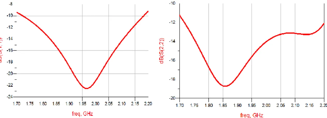
Figure 5 illustrates the variation plot of the input return loss (S11) in the frequency band 1.75GHz-2.15GHz. We observed that the parameter S11 varied between -11dB and -22.5dB. Thus, these values indicate a good input matching of the microwave PA over a wide-band and the reflection of the signal from the PA input to the source is low. The output matching can be determined by simulating the return loss (S22). Figure 6 shows the plot of this parameter. It can be observed that the output matching is good since S22 changes between 13.1dB and -18.7dB. So; the reflection of the signal from the PA output to the load is rather feeble.
Figure 5. Plot of the input reflection coefficient (S11) versus frequency
Figure 6. Plot of the output reflection coefficient (S22) versus frequency
TELKOMNIKA ISSN: 1693-6930
A Novel Configuration of a Microstrip Microwave Wideband Power Amplifier for… (A Rachakh) 229 The PA circuits must be stable in operating frequency band. That is primary to RF/microwave circuits, due to RF/microwave circuits would generate oscillation in someone operating frequency or some terminal conditions. These oscillations can raise the power gain of PA significantly and the active device could be damaged. thus, the important step to designing the power amplifier is to find the stability of the PA and combine the circuit components to ensure the stability in operating frequency band [15]. The PA can be considered as a two-port network that can be modelled by S parameter. thus, the absolute stability condition of PA can be determined by the Equations (5), (6) and (7) [16] and [17]:
11 22 12 21
1 | S | ² | S
| ² |
| ²
1
2 | S S
|
k
(5) 11 | S | ² | S
11 22| ² |
| ²
0
B
(6) 11 22 12 21|
| | S S
S S
|
(7)Where: k is the Rolett factor. B1 is the Stability measure.
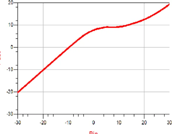
In order to satisfy the unconditional stability and assure an input/output matching at 50Ohm of microwave PA, a Taper line was added in series to improve the stability at the emitter path. This mean is easy to realize and the effect is better. Figure 7 represents the plots of the stability measure B1 and the stability factor K versus frequency. From Figure 7, it can be observed that B1>0 and K >1 over operating band 1.75GHz-2.15GHz. Thus, the conditions for unconditional stability are validated on the working frequency band. Therefore, there is no risk to get oscillations. We simulated the scattering parameters (Sij) to show the good functioning of the microwave PA in the frequency range 1.70GHz-2.20GHz. As shown in Figure 8, this study was conducted at 2GHz for power input range from -30 to 30dBm. The PA exhibits a saturated output power of 8dBm at 1dB compression point.
Figure 7. Plot of the stability measure B1 and the stability factor K versus
frequency
Figure 8. Input power versus output power for 2 GHz
5. Layout for Wideband Power Amplifier Circuit
The amplifier is printed on an FR4 substrate with a relative permittivity of 4.4 ,a thickness of 1.6mm, a metallization thickness t=0.035mm and a tangential loss of 0.025. The
proposed wide-band amplifier has an overall size of about 66 x 65.3mm². Figure 9 shows the Layout for the proposed PA.
Figure 9. Layout of proposed wide-band amplifier
Finally, we compared the proposed wideband power amplifier with other recently published articles on state-of-the-art of power amplifiers, the results are shown in Table 2. It can be remarked that the proposed wideband amplifier has considerably a power gain and reflection coefficients over a wider bandwidth than other PAs, which verifies the results show excellent performance of our design approach compared to the reported works.
Table 2. Comparision The Proposed Amplifier With other Recently Amplifiers
Parameter [18] [19] The Proposed
Amplifier
Process CMOS CMOS BJTs
Frequency (GHz) 1.65 to 2.00 1.70 to 3.10 1.75 to 2.15
Power Gain (dB) 5.15 9.8 110.5
Input Return Loss (dB) -21 -7 -22
Output Return Loss (dB) -8 - -18
6. Conclusion
In this paper, the proposed wide-band PA working from 1.75 GHz to 2.15 GHz had been designed. A microstrip technology has been utilized in the PA design in order to meet the design specification over the wide frequency ranges. The biasing circuits and matching impedance are also accurately designed so that the design specifications are met with lowest components. Optimization and tuning of the circuit are very important to confirm that the amplifier yields the excellent performance. The simulation results of the final Single stage PA illustrate that the power gain (S21) is above 11dB. The power gain was almost flat over the full band, the unilateral transmission (S12) less than 19dB, the input return loss S11 is between -11 and - 22dB, while the output return loss S22 ranges is between -13dB and -18dB. The proposed wide-band power amplifier has an average saturated output power of 8dBm at 1dB compression point and stability without oscillating in its required frequency band.
Acknowledgment
I would like to express my deep gratitude to Mr. Mohamed Latrach Professor in ESEO, engineering institute in Angers, France, for allowing us to use electromagnetic solvers available in his laboratory.
TELKOMNIKA ISSN: 1693-6930
A Novel Configuration of a Microstrip Microwave Wideband Power Amplifier for… (A Rachakh) 231 References
[1] AF Morabito, AR Laganà, G Sorbello, T Isernia. Mask-Constrained Power Synthesis of Maximally Sparse Linear Arrays througha Compressive-Sensing-Driven Strategy. Journal of Electromagnetic
Waves and Applications. 2015; 29(10): 1384-1396.
[2] AF Morabito, AR Lagana, T Isernia. Isophoric Array Antennas with a Low Number of Control Points: A 'Size Tapered' Solution. Progressin Electromagnetics Research Letters. 2013; 36: 121 131.
[3] Tsaraklimanis A, Karagianni E. Low Noise Amplifier Design for Digital Television Applications.
Journal of Electromagnetic Analysis and Applications. 2011; 03(07): 291-296.
[4] Munir A, Ranum B. Single Stage RF Amplifier with High Gain for 2.4GHz Receiver Front-Ends.
TELKOMNIKA (Telecommunication Computing Electronics and Control). 2014; 12(3): 711.
[5] Medley M. Microwave and RF circuits. Boston [u.a.]: Artech House; 1993.
[6] Niclas K, Wilser W, Kritzer T, Pereira R. On Theory and Performance of Solid-State Microwave Distributed Amplifiers. IEEE Transactions on Microwave Theory and Techniques. 1983; 31(6): 447-456.
[7] M Bacha, L Hadj Abderrahmane. Design of Broadband Microwave Amplifier for Telecommunication
Applications. The 14th IASTED International conference on Applied Simulation and Modelling.
Benalmadèna, Spain. 2005.
[8] Matthaei G, Young L, Jones E. Microwave filters, impedance-matching networks, and coupling structures. Norwood: Artech House. 1985.
[9] Tri T Ha. Solid State Microwave Amplifier Design. A Wiley Interscience Publication. 1981.
[10] Riblet G. Broad-band internally and externally matched lumped element symmetrical 5-ports. IEEE
Transactions on Circuits and Systems. 1985; 32(12): 1209-1213.
[11] R Beltran, FH Raab. Lumped-Element Output Networks For High-Efficiency Power Amplifiers. IEEE
MTT-S International Microwave Symposium, Anaheim, CA. 2010: 324~327.
[12] Martinez Mendoza M, Wentzel A, Alvarez Melcon A, Heinrich W. Advanced lumped-element filters for digital microwave power amplifiers. International Journal of Microwave and Wireless Technologies. 2015; 7(05): 589-596.
[13] Li Z, Guo B, Wei Z, Liu S, Cheng N, Wang J et al. A gain-flatness optimization solution for feedback technology of wideband low noise amplifiers. Journal of Zhejiang University SCIENCE C. 2011; 12(7): 608-613.
[14] Venkat Ramana. Aitha, Mohammad Kawsar Imam. Low Noise Amplifier for Radio Telescope at 1.42 GHz. Computer and Electrical Engineering, Halmstad University, Sweden, IDE0747. 2007: 29. [15] L. Samoska et al. On The Stability Of Millimeter-Wave Power Amplifiers. IEEE MTT-S International
Microwave Symposium Digest (Cat. No.02CH37278), Seattle, WA, USA, 2002; 1: 429-432.
[16] Chang K, Bahl I, Nair V. RF and microwave circuit and component design for wireless systems. New York: Wiley. 2002.
[17] Vendelin G. Design of amplifiers and oscillators by the S-parameter method. New York: Wiley. 1982; 200.
[18] H Aniktar, H Sjoland, JH Mikkelsen, T Larsen, A Class-AB 1.65GHz-2GHz Broadband CMOS Medium Power Amplifier. NORCHIP; 2005: 269-272.
[19] D Kalim, D Erguvan, R Negra, A 1.7 GHz-to-3.1 GHz Fully integrated broadband Class-E Power
Amplifier in 90 nm CMOS. 6th Conference on Ph.D. Research in Microelectronics & Electronics.