UV laser controlled quantum well intermixing in
InAlGaAs/GaAs heterostructures
J Genest1, J J Dubowski1*, V Aimez1, N Pauc1, D Drouin1 and M Post2 1
Regroupement québécois sur les matériaux de pointe (RQMP), Département de génie électrique et génie informatique, Université de Sherbrooke, Sherbrooke, Québec J1K 2R1, Canada; *Canada Research Chair in Quantum Semiconductors
2
Institute for Chemical Process and Environmental Technology National Research Council of Canada, Ottawa, Ontario K1A 0R6, Canada
E-mail: Jonathan.Genest@USherbrooke.ca
Abstract. The influence of surface irradiation of GaAs with a KrF excimer laser on the
magnitude of the quantum well intermixing (QWI) effect has been investigated on GaAs/AlGaAs and GaAs/AlGaAs/InAlGaAs QWs heterostructures. The selective area irradiation through a SiOx mask was carried out in an atmospheric environment. Following the
1000 pulses irradiation at 100 mJ/cm2, the samples were annealed in a rapid thermal annealing furnace at 900 ºC. Photoluminescence mapping and cathodoluminescence measurements show that significant laser-induced suppression of the QWI process can be achieved with lateral resolution of the order of 1 Pm.
1. Introduction
GaAs and InP based heterostructures are the material of choice for the fabrication of active photonic devices. However, the fabrication of photonic integrated circuits (PICs) requires the simultaneous integration of multiple bandgap structures within a single chip. In order to produce cost-effective PICs, selective area bandgap control of the heterostructure is of primary importance. Quantum Well Intermixing (QWI) is a leading post-growth approach to fabricate monolithic chips with areas of different bandgaps [1]. Among the numerous QWI techniques, UV-Laser controlled QWI is a new approach which has the potential to overcome common QWI techniques limitations primarily related to the control of the process.
The most frequently investigated methods of QWI include impurity induced intermixing [2], impurity-free vacancy diffusion [3] and QWI induced by ion implantation [4][5]. QWI has also been achieved by selective area coating of QW wafers with different oxides, nitrides and fluorides fabricated by conventional thin film deposition techniques [6]. Both enhanced [7] and reduced [8] intermixing has been observed depending on the physical and chemical properties of coating layers.
In this work, a KrF excimer laser has been used to suppress the intermixing in selected areas in GaAs/AlGaAs and GaAs/AlGaAs/InAlGaAs QWs heterostructures. Lateral resolution of this technique has also been investigated using photoluminescence (PL) mapping and cathodo-luminescence (CL).
605 © 2007 IOP Publishing Ltd
2. Experiment
2.1. QW wafers description
Two different QW structures were used for this work. The first one (Q1) consisted of two 7.5 nm thick GaAs quantum wells (QWs) separated by AlGaAs barriers. This structure was grown by molecular beam epitaxy on a n-type doped (100) GaAs substrate. It was designed for lasing operation at 852 nm at room temperature. Details of the structure are shown in table 1. The second heterostructure (Q2) was composed of a single 7 nm In0.1Al0.13Ga0.77As QW. The barriers were made of AlGaAs GRIN
layers. The second structure was also grown on a n-type GaAs substrate. This QW wafer was designed for lasing operation at 808 nm at room temperature. The table 2 shows Q2 specific details.
Table 1: Q1 layers composition and thickness
Composition Width (nm) Doping (cm-3) Dopant GaAs-p 100 7x10¹⁸ Zn Al.43Ga.57As-p 740 1.8x10 18 C Al.43Ga.57As 100 UD Al.23Ga.77As 54.4 UD GaAs (QW) 7.5 UD Al.23Ga.77As 10.3 UD GaAs (QW) 7.5 UD Al.30Ga.70As 147.9 UD Al.76Ga.24As 50 UD Al.73Ga.27As-n 45 1.7x10¹⁸ Se GaAs-n 100 1.7x10¹⁸ Se GaAs-n substrate Se
Table 2: Q2 layers composition and thickness
Composition Mole fraction Width (nm) Doping (cm-3) Dopant GaAs-p+ 200 3 x 10¹⁹ C AlxGa1-xAs x = 0.6 1500 1.1 x 10¹⁸ C AlxGa1-xAs (GRIN) x = 0.35 o 0.6 400 U/D InxAlyGa1-x-yAs (QW) x = 0.1; y = 0.13 7 U/D AlxGa1-xAs (GRIN) x = 0.6 o 0.35 400 U/D AlxGa1-xAs x = 0.6 1500 1018 Si AlxGa1-xAs (GRIN) x = 0.0 o 0.6 200 10 18 Si GaAs-n 200 1018 Si GaAs-n Subst. 2.2. Samples processing
Samples from both wafers were first cleaved and cleaned. A 200 nm thick silicon oxide was then deposited by the PECVD technique. Conventional photolithography and chemical etching were used to form patterned stripes and to process openings with widths changing from 200 µm down to 5 µm. Samples were then irradiated with a KrF excimer laser operating at 248 nm and delivering 22 ns long pulses at the rate of 3 Hz. The laser beam was shaped with a MicroLas microlens array (fly-eye) beam homogenizer [9],[10] to form a top-hat profile. This is done by averaging the localized intensity variations. All individual beamlets coming from the microlens array overlap in the focal plan.
The exposed area was 7 mm x 7 mm. Samples were irradiated in an atmospheric environment with 1000 pulses, each delivering a fluence of 100 mJ/cm2.
Following the laser irradiation, the samples went through a Rapid Thermal Annealing (RTA) step at 900°C. The RTA treatment consists of a 15 second ramping from room temperature to the annealing temperature and a 30 second anneal at a set temperature. The annealing was carried out in a hydrogen and nitrogen atmosphere while cooling was done under nitrogen.
2.3. Characterization
Photoluminescence (PL) mapping and Cathodoluminescence (CL) were used to characterize the modified bandgap energy and the lateral resolution of the UV laser controlled QWI technique. The PL mapping experiments were carried out at room temperature with a Philips PLM150 mapping system. A frequency doubled Nd:YAG laser (O = 532 nm) was used to excite the sample while the luminescence was dispersed by a monochromator and detected by an InGaAs photodiode array. The lateral resolution of this system was about 10 µm.
The CL experiments were performed with a LEO-55VP scanning electron microscope (SEM) under high vacuum. Both CL imaging and spectroscopy were achieved with a photomultiplier tube (PMT) that was used to detect the luminescence dispersed by a GATAN 300 mm monochromator. We
acquired monochromatic CL images in the fixed CL Wavelength Imaging mode (CLWI) to achieve spatial mapping of the QW emission.
3. Results and Discussion 3.1. PL mapping
Figure 1 shows the room temperature PL map of sample Q1 after KrF laser irradiation and annealing. We have previously demonstrated that the similar treatment of this material could reduce the blue shift of its bandgap by 22 nm in comparison to the non-treated material [11]. Here, the PL mapping shows a similar shift contrast of 20 nm between the masked and unmasked area. As shown in figure 2a), this contrast is not affected by the width of the openings. Note that a 5 µm line is difficult to resolve due to the limited lateral resolution of the experimental setup. Thus, we can conclude that the UV laser controlled QWI intermixing on this type of material is better than 10 µm.
Figure 1a) Room temperature PL mapping from sample Q1 after laser treatment and annealing. The dash line represents the position of the line scan. b) Wavelength histogram and legend.
Figure 2: Linescan from PL map of Q1. a) PL peak position b) PL FWHM
Figure 2b) shows that the PL peak full width at half maximum (FWHM) increases from 12 to 18 nm for the masked and unmasked region, respectively. Such broadening of the QW PL peak is usually attributed to the presence of defects in the QW vicinity [12], or to the development of stress in the active layer region [13]. Since defects diffusion in the QWs region is commonly known to enhance the intermixing process and thus to increase the recombination energy, we can associate the increase of
a) b)
the FWHM in the less blueshifted regions to the stress induced in the structure. Note that the edge effect on the line scan is caused by the superposition of signals from each side of the interface.
3.2. Cathodoluminescence
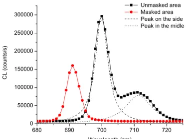
Since the active layers in Q2 are buried deeply under the structure surface and since the top layers are heavily doped, the room temperature PL signal from this wafer was below the detection limit of our PL setup. Low temperature (5K) CL was used to characterize the UV laser effect in the 5 µm width opening. Figure 3 shows the CL spectra from the masked and unmasked areas. The unmasked area spectrum exhibits two recombination peaks instead of one. Since the spatial origins of those two peaks are distinct (see figure 4a and b), this phenomenon is likely related to a diffraction effect. The diffraction effect could also explain the smaller QWI suppression (10 nm) in the edge area of the unmasked region compared to the 22 nm suppression in its center. This suggests the possibility of using phase shift masks for high resolution bandgap shifting.
680 690 700 710 720 0 50000 100000 150000 200000 250000 300000 Unmasked area Masked area Peak on the side Peak in the midle
C L (cou nts/ s) Wavelength (nm)
Figure 3: Low temperature CL spectra for the masked and unmasked area.
Figure 4 shows low-temperature CL wavelength images collected at 700, 712 and 690 nm. It can be seen that the transition between the masked and unmasked regions is approximately 1 µm wide. Given that this value is limited by the lateral width of the electron-matter interaction volume, which for the investigated heterostructure and at 20 kV is about 1 µm, we argue that the resolution of the UV laser controlled QWI intermixing process on this type of material is 1 Pm or better. However, CL signals coming from the laser exposed area also demonstrate an increase in their FWHM. It increases from 3.9 nm under the mask to 4.5 for the edge region to 9.7 nm for the less blueshifted area. These results are consistent with the stress driven explanation of the thermal shift.
Figure 4: Low temperature CL wavelength images at a) 700 nm, b) 712 nm and c) 690 nm. The white dashed lines show the frontier between the masked and unmasked regions.
4. Summary
It is demonstrated that KrF laser irradiation followed by RTA is an effective technique to suppress quantum well intermixing in GaAs/AlGaAs and GaAs/AlGaAs/InAlGaAs QWs heterostructures. The lateral resolution of this UV-Laser QWI technique has been evaluated to be about 1 µm or better.
This new process has the potential for the fabrication of multi-bandgap QW wafers processed with an excimer laser in a similar manner as the excimer-based photolithography for microelectronics. Alternatively, the ability to suppress the thermal shift using the excimer laser irradiation can be used in conjunction with other QWI approaches to create zones of materials with increased bandgap contrast and better control.
References
[1] Li E H 1998 SPIE milestones series MS 145
[2] Guido L J, Jackson G S, Plano W E, Hsieh K C, Holonyak Jr. N, Burnham R D, Epler J E, Thornton R L and Paoli T L 1987 Appl. Phys. Lett. 50 609-611
[3] J Teng J H, Dong J R, Chua S J, Thompson D A, Robinson B J, Lee A S W, Hazell J and Sproule I 2001 Mat. Sci. in Semicond. Processing 4 621–624
[4] Charbonneau S, Koteles E S, Poole P J, He J J, Aers G C, Haysom J, Buchanan M, Feng Y, Delage A, Yang F, Davies M, Goldberg R D, Piva P G and Mitchell I V 1999 IEEE J. Sel.Top.
Quantum Electron. 4 772-793
[5] Aimez V, Beauvais J, Beerens J, Morris D, Lim H S and Ooi B S 2002 IEEE J. Sel.Top.
Quantum Electron. 8, 870-879
[6] Yu J S., Song J D, Lee Y T and Lim H 2002 J. Appl. Phys. 92, 1386-1390
[7] Shimada N, Fukumoto Y, Uemukai M, Suhara T, Nishihara H and Larsson A 2001
Electronics-and-Communications-in-Japan,-Part-2-Electronics 87 34-42
[8] Beauvais J, Marsh J H, Kean A H, Bryce A C and Button C 1992 Electron Lett. 28 1670–1672 [9] Harvey E C , Rumsby P T 1997 Proceedings of SPIE 3223, 26
[10] Kahlert H J, Sarbach U, Burghardt B, Klimt B 1992, Proceedings of SPIE 1835, 112 [11] Genest J, Dubowski J J and Aimez V 2004 Proceedings of SPIE 5451, 550
[12] Marsh J H 1993 Semicond. Sci. Technol. 8 1136-1155
[13] Lee A S W, Li E H and Karunasiri G 1999 J. Appl. Phys. 86 3402-3407
Masked Masked Unmasked Masked Masked Unmasked Masked Masked Unmasked