Depletion layer imaging using a gaseous secondary electron detector in an
environmental scanning electron microscope
M. R. Phillips, M. Toth, and D. Drouin
Citation: Appl. Phys. Lett. 75, 76 (1999); doi: 10.1063/1.124281 View online: http://dx.doi.org/10.1063/1.124281
View Table of Contents: http://aip.scitation.org/toc/apl/75/1
Depletion layer imaging using a gaseous secondary electron detector
in an environmental scanning electron microscope
M. R. Phillipsa)and M. Toth
Microstructural Analysis Unit, University of Technology, P.O. Box 123, Broadway, NSW, 2007 Sydney, Australia
D. Drouin
De´partment de ge´nie electrique et ge´nie informatique, Universite´ de Sherbrooke, Sherbrooke, Que´bec, Canada, J1K 2R1
~Received 25 March 1999; accepted for publication 10 May 1999!
We present a method for imaging depletion layers using the gaseous secondary electron detector
~GSED! employed in environmental scanning electron microscopes. GSED images of a p-n
junction were obtained from a Si P1PN power diode. Behavior of the junction contrast as a function of imaging conditions is unrelated to reported GSED contrast formation mechanisms@ A. L. Fletcher, B. L. Thiel, and A. M. Donald, J. Phys. D 30, 2249 ~1997!#. Optimum imaging conditions are presented, and the contrast behavior is interpreted in terms of a previously unreported induced current component in GSED images. The presented technique is unique as it will enable imaging of depletion layers in uncoated semiconductor/oxide devices in controlled gaseous environments at elevated specimen temperatures. © 1999 American Institute of Physics.
@S0003-6951~99!01427-8#
Depletion layers at p-n junctions of semiconductor de-vices can be imaged in a scanning electron microscope
~SEM! using the electron beam induced current ~EBIC!
signal.1The boundary between p- and n-type regions can be observed using the voltage contrast2and capacitively decou-pled displacement current3 signals. Dopant contrast can be imaged in secondary electron ~SE! images obtained using a field emission gun SEM operated at a beam energy of ap-proximately 1 keV, where the SE yield maximizes.4,5In this letter, we report a method for depletion layer imaging using a previously unreported induced current signal component in SE images obtained using the gaseous secondary electron detector ~GSED!. The technique is unique in that it permits electron imaging of uncoated devices as a function of gas type and pressure~up to 20 Torr! as well as specimen tem-perature in an environmental SEM~ESEM!.
The ESEM can operate at specimen chamber pressures of up to 20 Torr.6 Conventional SEMs typically operate at chamber pressures of less than 1026Torr. Wide band gap materials cannot be imaged at accelerating voltages greater than a few kV without a grounded conductive coating due to localized specimen charging that causes: severe image dis-tortion, image drift, dielectric breakdown, flashover and de-flection of the primary electron beam.7 In the ESEM, the need for a conductive coating is eliminated by charge neu-tralization at the specimen surface by positive ions produced by ionization of gas molecules in the ESEM chamber by secondary, backscattered, and primary electrons.8 Gas ion-ization by SEs is utilized by the GSED for SE imaging in the ESEM. The GSED electron collector consists of a metallic ring held at a positive potential, VG, placed above the
speci-men. SEs emitted from the sample surface are accelerated to the detector ring, causing a gas ionization cascade that acts
as a high gain signal amplifier.8At a fixed gas pressure, P, and specimen-detector distance, d, the gain ~contrast in GSED images! is controlled by varying the magnitude of VG
~30–550 V!. The GSED is insensitive to light. It is therefore
possible to obtain high spatial resolution images at elevated specimen temperatures.
The specimen used in this study was a 1N4002 P1PN power diode, cross-sectioned parallel to the lead axis to ex-pose the silicon device and polished to an optical finish using diamond abrasives. GSED, EBIC, and absorbed current im-aging was performed using a W-gun FEI-Philips XL30 ESEM equipped with a GW Electronics type 31 specimen current meter. Water vapor was used as the gas in the ESEM chamber.
The location of the p-n junction within the Si device is shown in the mixed GSED/EBIC image, Fig. 1. The EBIC signal was measured by connecting both sides of the diode to ground. The n side was earthed through the specimen current meter. The p-n junction was not observed in images ob-tained using the GSED when both sides of the device were either open circuit or connected to ground. The junction can, however, be imaged using the GSED by making either the n-or p-side open circuit. Figures 2 and 3 show images of the
a!Corresponding author; electronic mail: [email protected]
FIG. 1. Mixed GSED/EBIC image of a cross-sectioned P1PN silicon power diode ~Ebeam520 keV, P51.9 Torr, horizontal field width 5289mm!.
APPLIED PHYSICS LETTERS VOLUME 75, NUMBER 1 5 JULY 1999
76
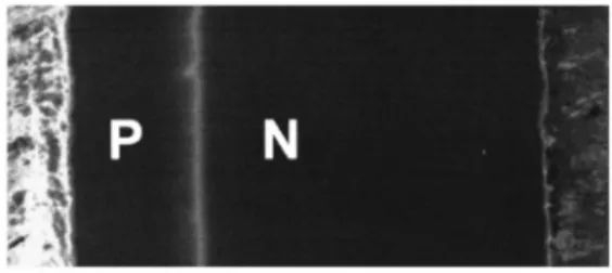
junction obtained with the p- and n-side open circuit, respec-tively. GSED images of the depletion region consist of dark and bright bands running parallel to the junction. As seen in Figs. 2 and 3, locations of the dark and bright bands with respect to the n- and p-sides of the junction depend on the wiring configuration~p- or n-side open circuit! and the scan direction~beam scanned from p to n or from the n to p side!. The junction contrast in GSED images is most pronounced when P and d are minimized and the scan speed is maxi-mized. The presence of depletion layer contrast in GSED images is independent of the magnitude of VG~0 V, 30–550
V!. The contrast is not present under any image acquisition conditions when the electron beam is scanned parallel to the junction.
Contrast in low voltage SE images of flat semiconductor samples that exhibit no atomic number contrast has been
attributed to electronic effects that cause dopant sensitive changes in the SE yield. Increases in the SE yield of p-type regions and decreases in n-type regions have been explained by band bending due to surface state pinning of the Fermi level.4If the junction contrast observed in the GSED images in Figs. 2 and 3 was related to changes in SE emission, an increase in d and VGshould enhance the GSED signal due to
an increase in gas ionization cascade amplification. The con-trast should maximize at the chamber pressure corresponding to the maximum of the gas gain curve,8not when P and d are minimized. The observed contrast behavior therefore cannot be explained by current models of contrast formation in GSED images.8
Absorbed current images obtained with the p-side open circuit and the n-side connected to ground through the am-meter are shown in Fig. 4. Images obtained with the n-side open circuit are shown in Fig. 5. Figures 4~a! and 5~a! were obtained by scanning the electron beam from the p to the n side of the junction. The scan direction was reversed to ob-tain the images in Figs. 4~b! and 5~b!. As in the GSED im-ages, the junction consists of a pair of bands running parallel to the junction in each image. The location of the dark and bright bands with respect to the n and p side of the junction depend on the diode wiring configuration and the scan direc-tion.
We attribute the junction contrast to an induced current component in GSED images caused by charging and dis-charging of the open circuit side of the diode during image acquisition. When a scanning electron beam impinges on the depletion region, the junction contact potential charge-separates electron-hole pairs excited by primary electrons. Electrons and holes are injected into the n and p sides, re-spectively. When the beam is scanned from the p to the n side, the p side is open circuit and the n side is grounded, electrons are injected into the n-side flow to earth. The charge flow produces the bright band on the p side of the junction in the absorbed current image in Fig. 4~a!. Holes injected into the p side cause a net positive charge buildup
FIG. 2. GSED images of the diode obtained with the p-side open circuit and the n side connected to ground. During image acquisition, the electron beam was scanned~a! from the p to the n side and ~b! from the n to the p side (Ebeam520 keV, P51.9 Torr, horizontal field width5289mm!.
FIG. 3. GSED images of the diode obtained with the n-side open circuit and the p side connected to ground. During image acquisition, the electron beam was scanned~a! from the p to the n side and ~b! from the n to the p side (Ebeam520 keV, P51.9 Torr, horizontal field width5289mm!.
FIG. 4. Absorbed current images of the diode obtained with the p-side open circuit and the n side connected to ground. During image acquisition, the electron beam was scanned~a! from the p to the n side and ~b! from the n to the p side~Ebeam520 keV, P51.9 Torr, horizontal field width5289mm!.
77
and forward bias the device. The resulting electric field in-duces electron flow from the GSED preamplifier to the col-lector ring, producing the dark band on the p side of the junction in the GSED image shown in Fig. 2~a!. A ‘‘bright’’ signal in GSED images corresponds to flow of electrons from the collector ring to the GSED preamplifier. As the beam continues to scan across the junction ~to the n side!, electrons are injected into the p side and neutralize the posi-tive charge through electron-hole recombination. The result-ing dissipation of positive charge induces a flow of electrons from the GSED collector ring to the GSED preamplifier, producing the bright band on the n side of the junction in the GSED image in Fig. 2~a!. To maintain charge neutrality, the flow of electrons to the p side is compensated by a flow of electrons to the sample through the grounded n side of the device, producing the dark band on the n side of the junction in the absorbed current image in Fig. 4~b!.
When the beam is scanned from the n to the p side of the junction ~with the p-side open circuit!, the dark band in the GSED image@Fig. 2~b!# and the bright band in the absorbed current image @Fig. 4~b!# appear on the n side, due to the
positive charging and discharging of the p side of the diode. When the n side is open circuit and the p side is grounded through the ammeter, the band contrast in GSED~Fig. 3! and absorbed current~Fig. 5! images is reversed with respect to the case described above~p-side open circuit! due to nega-tive charging and discharging of the n side of the device as the beam is scanned across the junction. Detail in the con-trast on the p side of the junction in all GSED and absorbed current images of the depletion layer is caused by the pres-ence of a P1P junction in the power diode.
The proposed induced contrast model can now be used to explain the behavior of the depletion layer contrast as a function of imaging conditions. A decrease in P or d en-hances the junction contrast due to a corresponding increase in the magnitude of the electric field produced at the GSED collector ring by charging of the open circuit side of the device. The magnitude of the current induced in the GSED collector ring maximizes when the rate of change of the os-cillating electric field produced by charging and discharging of the open circuit side of the device is maximized. The contrast is therefore most pronounced at high scan rates and it is not present in images obtained by scanning the electron beam parallel to the junction.
In conclusion, this letter presents a method for imaging of depletion layers using a GSED in an ESEM. Coupled with the ESEM hot stage, the technique will allow in situ imaging of depletion layers in uncoated samples, such as metal-oxide-semiconductor~MOS! devices, in the controlled gaseous en-vironment of an ESEM chamber at elevated specimen tem-peratures. The junction contrast was interpreted using a previously unreported induced current signal component in GSED images.
1D. B. Holt, SEM Microcharacterization of Semiconductors ~Academic, London, 1989!, p. 241.
2
S. M. Davidson, SEM Microcharacterization of Semiconductors ~Aca-demic, London, 1989!, p. 153.
3E. I. Rau and V. N. E. Robinson, Microsc. Microanal. 3, 495~1997!. 4D. D. Perovic, M. R. Castell, A. Howie, C. Lavoie, T. Tiedje, and J. S. W.
Cole, Ultramicroscopy 58, 104~1995!. 5
D. C. Houghton, Appl. Phys. Lett. 69, 1593~1996!. 6G. D. Danilatos, Mikrochimica Acta 114/115, 143~1994!.
7J. I. Goldstein, D. E. Newbury, P. Echlin, D. C. Joy, A. D. Romig, Jr., C. E. Lyman, C. Fiori, and E. Lifshin, Scanning Electron Microscopy and Microanalysis~Plenum, New York, 1992!, p. 671.
8A. L. Fletcher, B. L. Thiel, and A. M. Donald, J. Phys. D 30, 2249~1997!. FIG. 5. Absorbed current images of the diode obtained with the n-side open
circuit and the p side connected to ground. During image acquisition, the electron beam was scanned~a! from the p to the n side and ~b! from the n to the p side~Ebeam520 keV, P51.9 Torr, horizontal field width5289mm!.