ETUDE ELECTRO-OPTIQUE DE LTNTERFACE
«-ALCANETfflOLS GaAs(OOl): LES PHENOMENES DE
SURFACE ET LES APPLICATIONS EN
BIO-DETECTION A BASE DE PHOTOLUMINESCENCE
ELECTRO-OPTIC INVESTIGATION OF THE
/i-ALKANETHIOL GaAs(OOl) INTERFACE: SURFACE
PHENOMENA AND APPLICATIONS TO
PHOTOLUMINESCENCE-BASEDBIOSENSING
These de doctorat
Specialite: Genie electrique
Composition du jury:
Prof. Jan J. Dubowski, Universite de Sherbrooke, directeur
Dr. Farid Bensebaa, National Research Council of Canada, co-superviseur
Prof. Frank Traeger, University of Kassel, expert externe
Dr. Gregory P. Lopinski, National Research Council of Canada, expert externe
Prof. Dominique Drouin, Universite de Sherbrooke, rapporteur
© Gregory M. Marshall
Universite de Sherbrooke
Faculte de genie
Departement de genie electrique
et de genie informatique
Ill
Library and Archives Canada Published Heritage Branch 395 Wellington Street Ottawa ON K1A 0N4 Canada Bibliotheque et Archives Canada Direction du Patrimoine de I'edition 395, rue Wellington Ottawa ON K1A 0N4 CanadaYour file Votre reference ISBN: 978-0-494-83274-5 Our file Notre reference ISBN: 978-0-494-83274-5
NOTICE:
The author has granted a
non-exclusive license allowing Library and Archives Canada to reproduce, publish, archive, preserve, conserve, communicate to the public by
telecommunication or on the Internet, loan, distrbute and sell theses
worldwide, for commercial or non-commercial purposes, in microform, paper, electronic and/or any other formats.
AVIS:
L'auteur a accorde une licence non exclusive permettant a la Bibliotheque et Archives Canada de reproduire, publier, archiver, sauvegarder, conserver, transmettre au public par telecommunication ou par I'lnternet, preter, distribuer et vendre des theses partout dans le monde, a des fins commerciales ou autres, sur support microforme, papier, electronique et/ou autres formats.
The author retains copyright ownership and moral rights in this thesis. Neither the thesis nor substantial extracts from it may be printed or otherwise reproduced without the author's permission.
L'auteur conserve la propriete du droit d'auteur et des droits moraux qui protege cette these. Ni la these ni des extraits substantiels de celle-ci ne doivent etre imprimes ou autrement
reproduits sans son autorisation.
In compliance with the Canadian Privacy Act some supporting forms may have been removed from this thesis.
While these forms may be included in the document page count, their removal does not represent any loss of content from the thesis.
Conformement a la loi canadienne sur la protection de la vie privee, quelques formulaires secondaires ont ete enleves de cette these.
Bien que ces formulaires aient inclus dans la pagination, il n'y aura aucun contenu manquant.
RESUME
Les surfaces de semi-conducteur couplees a des structures moleculaires derivees de la chimie organique forment la base d'une nouvelle classe emergeante de dispositifs a effet de champ. En plus de la recherche dans le domaine d'electronique moleculaire, ces interfaces sont developpees pour une variete d'applications de biosenseur en electronique et en optique. Les monocouches auto-assemblees (SAMs) composees de n-alcanethiols [HS(CH2)„R] qui se couplent a la surface de GaAs(OOl) par la formation de la liaison covalente S-GaAs sont d'un interet pratique. Ces SAMs offrent des fonctionnalites potentielles en termes de chimie requise pour les senseurs et de 1'effet de passivation de tel couplage.
Dans cette these, l'interface SAM-GaAs est etudiee dans le cadre de biosenseur photonique base sur la variation de la photoluminescence (PL). Le plan de cette recherche est classe en trois parties : i) l'analyse structurelle et compositionnelle de la surface en utilisant la spectroscopic de photoelectrons induits par rayons X (XPS), ii) l'etude des proprietes electroniques a l'interface sous les conditions d'equilibre en utilisant la spectroscopie infrarouge (IR), la methode de la sonde de Kelvin et XPS et iii) l'analyse de la reponse electro-optique sous l'excitation photonique permanente, en particulier, le photovoltage de surface (SPV) et l'intensite de la PL.
En utilisant un modele de recouvrement partiel de spectres de la resolution angulaire XPS dans lequel les attributions des composantes sont demontrees etre quantitativement valides, le taux du recouvrement de la terminaison methyle du SAM est demontree exceder 90%. Parmi les resultats remarquables, c'est l'obtention d'une surface riche en Ga, pauvre en oxyde, et dont l'As elementaire est present en quantites sous-monocouches en accord avec la theorie des morphologies surfaciques. L'analyse modale de la transmission des spectres de l'IR montre que l'ordre moleculaire des SAMs est suffisant pour permettre la deduction (selon la loi de Beer-Lambert) des constantes optiques IR, ce qui mene a I'observation d'une augmentation
d ' s b s o r b s n c e SneC!fic,l.!C dpS S A M s P^f !? CO^fH^t'O1! d f I'ah<;nrhanrp TR swpr* le nntpntipl HP la
couche dipolaire de SAM, le mecanisme de P augmentation est attribue aux moments vibrationnels ajoutes par la polarisation electronique dans le champ statique des SAMs. Enfin, la position du niveau de Fermi a la surface est determinee par XPS et est utilisee pour interpreter les resultats de SPV en termes de reduction de la section transversale a la surface pour la capture des porteurs minoritaires, induite par les thiols. L'analyse numerique confirme ce resultat base sur la theorie de transport de porteur de l'intensite de la PL dans le contexte d'une reduction de la vitesse de recombinaison a la surface.
Mots cles : photonique, biosenseur, GaAs, monocouches auto-assemblees, spectroscopie de photoelectrons induits par rayons X, spectroscopie infrarouge, photoluminescence, niveau de Fermi, photovoltage.
ABSTRACT
Semiconductor surfaces coupled to molecular structures derived from organic chemistry
form the basis of an emerging class of field-effect devices. In addition to molecular
electronics research, these interfaces are developed for a variety of sensor applications in the
electronic and optical domains. Of practical interest are self-assembled monolayers (SAMs)
comprised of «-alkanethiols [HS(CH2)„R], which couple to the GaAs(OOl) surface through
S-GaAs covalent bond formation. These SAMs offer potential functionality in terms of the
requisite sensor chemistry and the passivation effect such coupling is known to afford.
In this thesis, the SAM-GaAs interface is investigated in the context of a photonic
biosensor based on photoluminescence (PL) variation. The scope of the work is categorized
into three parts: i) the structural and compositional analysis of the surface using X-ray
photoelectron spectroscopy (XPS), ii) the investigation of electronic properties at the interface
under equilibrium conditions using infrared (IR) spectroscopy, the Kelvin probe method, and
XPS, and iii) the analysis of the electro-optic response under steady-state photonic excitation,
specifically, the surface photovoltage (SPV) and PL intensity.
Using a partial overlayer model of angle-resolved XPS spectra in which the component
assignments are shown to be quantitatively valid, the coverage fraction of methyl-terminated
SAMs is shown to exceed 90%. Notable among the findings are a low-oxide, Ga-rich surface
with elemental As present in sub-monolayer quantities consistent with theoretical surface
morphologies. Modal analysis of transmission IR spectra show that the SAM molecular order
is sufficient to support a Beer-Lambert determination of the IR optical constants, which yields
the observation of a SAM-specific absorbance enhancement. By correlation of the IR
absorbance with the SAM dipole layer potential, the enhancement mechanism is attributed to
the vibrational moments added by the electronic polarizability in the static field of the SAM.
Lastly, the surface Fermi level position is determined by XPS and is used to interpret SPV
results in terms of a thiol-induced reduction of the surface cross-section for minority
carrier-capture. Numerical analysis confirms this result based on the carrier transport theory
of PL intensity by means of a reduction of the surface recombination velocity.
Keywords: photonics, biosensor, GaAs, self-assembled monolayers, X-ray photoelectron
SUMMARY of ORIGINAL CONTRIBUTIONS
The content of this thesis is attributed to the author as unpublished work, and as pending
or published scientific literature as follows: 1) Journal of Applied Physics, "Observation of
surface enhanced IR absorption coefficient in alkanethiol based self-assembled monolayers on
GaAs(OOl)" [Marshall et al, 2009a], 2) Langmuir, "Surface Dipole Layer Potential Induced
IR Absorption Enhancement in H-Alkanethiol SAMs on GaAs(OOl)" [Marshall et al., 2009b],
3) Applied Surface Science, "Surface barrier analysis of semi-insulating and n -type
GaAs(OOl) following passivation with w-alkanethiol SAMs" [Marshall et al., 2011a],
4) Nanotechnology, "Electro-optic investigation of the surface trapping efficiency in
rc-alkanethiol SAM passivated GaAs(OOl)" [Marshall et al, 201 lb], and as contributed in 5)
Journal of Applied Physics, "Formation dynamics of hexadecanethiol self-assembled
monolayers on (001) GaAs observed with photoluminescence and Fourier transform infrared
spectroscopies'" [Kim et al, 2009], and 6) Applied Surface Science, "Molecular self-assembly
and passivation of GaAs (001) with alkanethiol monolayers: A view towards
bio-functionalization" [Dubowski et al., 2010].
ACKNOWLEDGEMENTS
The author wishes to acknowledge the Universite de Sherbrooke and the National
Research Council of Canada (NRC), Institute for Chemical Process and Environmental
Technology (ICPET) for supporting an extended secondment to ICPET as a Visiting Worker.
This opportunity allowed a rich variety of research topics to be pursued and provided access
to helpful subject matter expertise. Thanks is also given to the NRC for financial support,
including the Graduate Student Scholarship Supplement Program award, and to the Faculte de
Genie for accepting graduate course transfer credits from the University of Ottawa.
Appreciation is extended to the director of this work, Prof. Jan J. Dubowski, for financial
support, the opportunity to develop the contents of this work to its potential, and for
accommodating concurrent obligations to the Canadian Forces Army Reserve. Special thanks
are given to Dr. Farid Bensebaa (ICPET), who provided functional supervision, operational
support and valuable career mentorship, and to Dr. Gregory P. Lopinski of the NRC Steacie
Institute for Molecular Sciences, with whom insightful technical discussions and productive
collaborations were the result of much generosity.
The camaraderie, peer learning and technical support offered by several members of Prof.
Dubowski's group and members of the ICPET staff are also gratefully acknowledged,
especially: Mr. David Kingston, Dr. Ximing Ding, Dr. Oleksandr Voznyy, Dr. Radoslaw
Stanowski, Dr. Chan Kyu Kim, Dr. Khalid Moumanis, Dr. Palani Arudra and Dr. Jianfu Ding.
TABLE of CONTENTS
RESUME i ABSTRACT ii SUMMARY of ORIGINAL CONTRIBUTIONS iii
ACKNOWLEDGEMENTS iv TABLE of CONTENTS v LIST of FIGURES viii LIST of TABLES xii ACRONYMS xiii CHAPTER 1: INTRODUCTION 1
1.1 Fundamentals of Biosensing 1 1.2 Surface Chemistry and Molecular Self-Assembly 4
1.3 Semiconductor-based Biosensing 8 1.3.1 Channel Conductance Methods 8 1.3.2 Photoluminescence Methods 11 1.4 Motivations and Research Objectives 15
1.4.1 Structural and Chemical Characterization 15
1.4.2 Electronic Properties of the SAM 16 1.4.3 Electro-Optic Response of the GaAs Interface 16
1.5 Structure of the Thesis 17 CHAPTER2: LITERATURE and THEORY 19
2.1 X-ray Photoelectron Spectroscopy of the SAM-GaAs Interface 19
2.1.1 Surface Composition and Passivation of GaAs 22
2.1.1.1 Inorganic Sulphides 24 2.1.1.2 Organic Thiols 25 2.1.1.3 Oxide Etching 29 2.1.1.4 SAM-GaAs Interface Structure 30
2.1.2 Angle-Resolved XPS Methods 31
2.1.3 Surface Energy Levels 34 2.2 infrared Spectroscopy and Moiecuiar Ordering in the SAM 37
2.2.1 Quantum Mechanics of the IR Absorption Intensity 39 2.2.2 Polarizability and the Principal Components of the Refractive Index 42
2.2.3 Molecular Structure and Orientation of the SAM 45 2.2.4 Symmetry and the Optical Constants in IR Modeling of the SAM 47
2.3 Surface Energy Levels by the Kelvin Probe Method 49
2.3.1 Work Function Measurements 49 2.3.2 Surface Photovoltage and the Surface Barrier Height 53
2.3.2.1 Excess Carrier Screening of the Space Charge Region 53
2.3.2.2 Surface Charge Modification 55 2.3.2.3 Equilibrium Band-Bending in SPV and PL Models 58
2.4 Photoluminescence of the SAM-GaAs Interface 59 2.4.1 Near-Surface Model of the Photoluminescence 59 2.4.2 Sensor Operation Based on the Dead-Layer 61
2.4.3 Non-Radiative Recombination Theory 63
2.5 Chapter Summary 67 CHAPTER 3: COMPOSITION and STRUCTURAL ANALYSIS by XPS 68
3.1 Experimental Detai Is 68 3.1.1 Sample Preparation 68
3.1.1.1 Wafer Cleaning 68 3.1.1.2 Ethanol Solvent Degassing 69
3.1.1.3 Preparation of Thiol Solution 69 3.1.1.4 Etching and SAM Incubation 70
3.1.2 Recording of XPS Spectra 70 3.1.3 Component Fitting with CasaXPS Software 71
3.2 Spectra and Compositional Stoichiometry 72
3.2.1 GaAs Survey 72 3.2.2 GaAs High-Resolution 75
3.2.3 HDT-SAM Prepared GaAs 80 3.2.4 Compositional Analysis of XPS Data 85
3.3 Angle-Resolved XPS Structural Analysis 87 3.3.1 GaAs Surface Stoichiometry 87 3.3.2 Surface Concentration of Elemental Arsenic 89
3.3.3 Fractional Coverage of the SAM 91
3.4 Chapter Summary 94 CHAPTER 4: INFRARED SPECTROSCOPY of the SAM 95
4.1 Experimental Detai Is 95 4.1.1 SAM Preparation 95 4.1.2 Liquid Thiol for Beer-Lambert Analysis 96
4.1.3 IR Transmission Measurements 96 4.2 Modal Analysis and Observation of SAM Formation Dynamics 97
4.2.1 Modal Analysis of Methyl-Terminated Alkanethiols 97
4.2.2 Formation Dynamics 102 4.3 Beer-Lambert Analysis of the IR Absorption 103
4.3.1 Evaluation of the Absorption Coefficient 103
4.3.2 Absorption Enhancement Effect 106
4.4 Optical Constants of the SAM 107 4.5 Amine-Terminated Alkanethiols 110
4.6 Chapter Summary 113 CHAPTER 5: SURFACE BAND STRUCTURE in EQUILIBRIUM 114
5.1 Experimental Detai Is 114 5.1.1 Kelvin Probe and XPS Work Function Measurements 1 14
5.1.2 Baseline Thermal Disordering of the SAM 115 5.1.3 Integration of Au Binding Energy Calibrant 116
5.2 Dipole Layer Potential of the SAM 117 5.2.1 Motivations in the Context of IR Enhancement 1 17
5.2.2 Discussion on Fermi Level Pinning 118 5.2.3 Work Function and the Dipole Layer Potential 120
5.2.3.2 IR Spectroscopy of the Disordered SAM 122
5.2.3.3 XPS Determination of the DLP 123 5.2.4 DLP and the Effective Capacitor Model 125 5.2.5 Correlation with the IR Absorbance and the IR Enhancement Effect 127
5.3 Surface Barrier Analysis following SAM Passivation 134 5.3.1 XPS Results of the Surface Fermi Level 134 5.3.2 Surface Barrier Height and the AUDM 138
5.4 Chapter Summary 141 CHAPTER 6: NEAR-SURFACE ELECTRO-OPTIC PHENOMENA 142
6.1 Experimental Details 143 6.1.1 Sample Preparation 143 6.1.2 Surface Photovoltage Measurements 143
6.1.3 Photoluminescence Measurements 143 6.2 Surface Photovoltage of SAM Passivated GaAs 144
6.2.1 SPV Results 144 6.2.2 SPV Model Parameters 145
6.2.3 Scale Transformation to Photon Irradiance 148 6.2.4 Surface Carrier Capture Coefficients 149
6.2.5 Discussion of SPV Findings 151 6.3 Photoluminescence of SAM Passivated GaAs 153
6.3.1 PL Enhancement in the Flat-Band Regime 153 6.3.2 Transport Model of PL Enhancement 158
6.3.3 Discussion of PL Results 160
6.3.4 Null Enhancement of n+GaAs 161
6.4 Significance to the Operation of a Biosensor 162
6.5 Chapter Summary 165 CHAPTER 7: THESIS SUMMARY and CONCLUDING REMARKS 166
7.1 Thesis Summary 166 7.2 Concluding Remarks 169 APPENDIX A 171 APPENDIX B 173 APPENDIX C i7t> APPENDIX D 179 APPENDIX E 180 APPENDIX F 182 BIBLIOGRAPHY 183
LIST of FIGURES
Figure 1.1. Generalization of biosensing concept 2 Figure 1.2. COOH-terminated alkanethiol SAM used for dopamine
recognition via electrostatic discrimination on a gold voltammetric
electrode 6 Figure 1.3. OH-terminated and biotinylated polyether thiols form mixed
molecule SAMs for streptavidin immobilization 7 Figure 1.4. HEMT design MOCSER with porphyrin-based SAM used for
the detection of nitric oxide in physiological aqueous solutions 10
Figure 1.5. Recombination processes in GaAs 11 Figure 1.6. Near-surface band structure of n-type GaAs in depletion 13
Figure 2.1. Pictorial descriptions of basic XPS theory 21 Figure 2.2. Chemical passivation of GaAs surface with a bio-functional
alkanethiol SAM 23 Figure 2.3. As 3d and Ga 3d core level photoelectron spectra of the (NFLO2S
passivated GaAs(001) surface 24 Figure 2.4. Regions of the SAM-GaAs interface used for evaluation of the
surface sensitivity ratio 27 Figure 2.5. Ga 3d, As 3d and S 2p core level photoelectron spectra of the
ODT passivated GaAs(001) surface 28 Figure 2.6. SAM matched GaAs(OOl) reconstruction according to molecular
simulations 31 Figure 2.7. Schematic of ARXPS of an overlayer (L) on substrate (S) 32
Figure 2.8. Energy level diagram of various materials in an XPS experiment 35
Figure 2.9. Normal vibrational modes of the water molecule 38 Figure 2.10. Energy well models describing the diatomic potential as a
function of internuclear separation 40 Figure 2.11. Molecular coordinates of the SAM defined by the tilt (9) of the
C-C-C backbone piane, the azimuth with respect to the cubic iattice, and the
twist orientation (\|/) about the molecular axis 45 Figure 2.12. Factors contributing to the work function potential of a
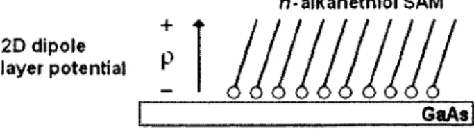
semiconductor n-type surface 50 Figure 2.13. Energy level diagrams illustrating the establishment of the
CPD 51 Figure 2.14. Illustration of the 2D dipole layer potential formed by a
self-assembled monolayer on the GaAs(OOl) surface, after Marshall et al.
[Marshall e/ ai, 2009b] 51 Figure 2.15. CPD as a function of molecular chain length for methyl
Figure 2.16. Calculated SPV (solid lines) as a function of the excess carrier density for n-type GaAs under the assumed condition that the surface charge
density (-qNt) remains constant 55
Figure 2.17. Calculated SPV as a function of the excess carrier density for n-type GaAs with a discrete level acceptor state located at £, and having
surface density N, 57 Figure 2.18. Shockley-Reed-Hall recombination Unr for a trap level E,
located within the band-gap of GaAs for various values of j 65 Figure 3.1. Low resolution XPS survey spectrum of etched only
semi-insulating GaAs(OOl) at ToA = 0° 73 Figure 3.2. As per Figure 3.1 showing LMM Auger bands due to Ga and As 73
Figure 3.3. As per Figure 3.1 showing loss peaks characteristic of the GaAs
volume plasmon at +15.6 eV from the parent photoemission line 74 Figure 3.4. High resolution XPS spectra from the elements identified in
Figure 3.1 at ToA - 60° 77 Figure 3.5. NH4OH etched GaAs following Ar-ion in situ sputtering 80
Figure 3.6. XPS spectra of unbound molecular thiol, Au bonded thiolate, and the Au film used for Fermi level referenced calibration of the binding
energy to Au 4f7/2 at 84.00 eV , 81
Figure 3.7. High resolution XPS spectra from semi-insulating GaAs
prepared with HDT-SAM. ToA = 60° 82 Figure 3.8. Comparison of etched only GaAs and as prepared with
HDT-SAM in the As 3d region 84 Figure 3.9. ARXPS data of As:Ga ratio and model analysis according to
Equations 3.2 and 3.4 for HDT-SAMs 88 Figure 3.10. Fractional overlayer model of the corrugated surface 89
Figure 3.11. Fractional overlayer model of As° coverage on GaAs prepared
with HDT-SAM 91 Figure 3.12. Fractional overlayer model of HDT-SAM coverage on GaAs 92
Figure 4.1. Illustration of the technique used to quantify the absorption thickness of a thin layer of liquid thiol pressed between two coverglass
slides 96 Figure 4.2. In transmission mode, SAMs present absorption path length
differences ( A / ) dictated by the length of their respective molecules 97 Figure 4.1. Transmission IR spectra of «-alkanethiol [HS(CH2)nCH3] SAMs
onGaAs(OOl) 98 Figure 4.4. Component analysis of IR spectra 100
Figure 4.5. CH2 asymmetric mode peak frequency vs. modal scale factor; continuous model (line), component fit results (circles), illustrating the
Figure 4.6. IR peak absorbance (a), and position (b), of the asymmetric C-H
stretching mode of alkane CH2 in HDT-SAMs 102 Figure 4.7. CHh asymmetric mode amplitude as a function of the methylene
number (circles) 103 Figure 4.8. Liquid phase C-H stretching mode spectra: (a) «13 / 11 urn, (b)
«9 / 8 urn and (c) «13 / 4 urn, according to layer thickness 105 Figure 4.9. Enhancement factor observed for the SAM phase absorption
coefficient relative to Beer-Lambert measurements in bulk material 105 Figure 4.10. Comparison of the principal components of the refractive index
determined using Beer-Lambert analysis in the present work (a) and (b) [Marshall et ah, 2009b], with results from IR ellipsometry adapted from
Rosue/a/. [Kosuetai, 2009] (c) and (d) 109 Figure 4.11. Comparison of methyl-terminated alkanethiol SAMs HDT and
DDT with amine-terminated SAMs of similar length (methylene numbers
/i = 16 and II) I l l Figure 4.12. XPS spectra of n i l ATA-SAMs on GaAs 112
Figure 5.1(a). Kelvin Probe (KP) CPD (squares) and asymmetric CH2 stretching mode peak IR absorbance (circles) vs. chain length for
[HS(CH2)„CH3] SAMs on semi-insulating GaAs(OOl) 121
Figure 5.1(b). CPD for SAMS as per (a) on heavily Si-doped (n+-type)
GaAs 121 Figure 5.2. C-H stretching mode IR spectra in transmission of «15-SAM
before and after thermal disordering in 55°C isopropanol (IPA) 122 Figure 5.3. XPS core level As 3d spectra at 0° ToA from etched but
untreated GaAs (left) and from GaAs prepared with «I5-SAM (right) 123 Figure 5.4. Generalized band diagram of the XPS measurement in Figure
5.3 showing a reduction of the electron affinity (EA) associated with the surface dipole moments of the SAM (arrows) that result in an increase of the
core level (CL) energies 124 Figure 5.5. XPS core level S 2p / Ga 3s spectra of «15-SAM before (left)
A „ f t „ - t U „ „ „ „ l A'.r.nrAn-.nn {*.\„Ut\ IOC U I 1 1 4 U H V I U I V 1 I 1 I C 4 1 V l l t j v y i v t v i » i « * i y i » £ j * * V • —
-5.6. Calculated DLP assuming molecular dipole values in a SAM of non-interacting / surface independent alkanethiols (squares). DLPs evaluated
from CPD measurements (circles) for SAMs on semi-insulating GaAs(OOl) 126
Figure 5.7. Method of calculating the Lorentz local field correction 131 Figure 5.8. Relative IR absorbance of the asymmetric C-H stretching mode
of methylene in rc-alkanethiol SAMs on Au (squares) and GaAs(OOl)
(circles) vs. the SAM DLP 133 Figure 5.9. XPS As 3d core level and valence band regions of
semi-insulating GaAs for samples: (circles) passivated with «15-SAM, and
Figure 5.10. XPS spectra: (a) Au 4f peaks labeled with spin-orbit branching, and (b) the O Is region including spectra following passivation with «15-SAM (lower series) and from the etched and reoxidized GaAs reference
surface (upper series), shifted vertically for clarity 135 Figure 5.11. Energy level diagram illustrating the XPS binding energy
referencing used to determine the surface FL position above the VBE 136 Figure 5.12. (a) Ionized charge centre concentrations for the EL2 donor
(solid) and carbon acceptor (dotted) defect levels in undoped semi-insulating
GaAs 139 Figure 6.1. Kelvin Probe SPV measurements on: (a) semi-insulating GaAs;
etched only (solid), as prepared with «15-SAM (dash-dot) 144 Figure 6.2. Schematic comparison of the AUDM-based surface Fermi level
(FL) position in Ga-rich n-doped and semi-insulating GaAs 146 Figure 6.3. Surface FL pinning places an upper boundary on the surface
charge density as the energy density of surface states approaches the discrete
limit 147 Figure 6.4. SPV data (circles) and model results (solid lines) for
semi-insulating GaAs before and after passivation with nl5-SAM 149 Figure 6.5. SPV data and model results for n+-GaAs before and after
passivation with n 15-SAM 150 Figure 6.6. Schematic of the electric field profiles for: i) the built-in field of the
SCR, partially screened under illumination, and ii) the penetrating interfacial dipole
layer potential 152 Figure 6.7. Relative PL efficiency as a function of the excitation power for
semi-insulating GaAs before (circles) and after (squares) preparation with
«15-SAM 154 Figure 6.8. Calculated PL enhancement ratio for semi-insulating GaAs
following passivation with «15-SAMs as a function of the nominal SRV
(S) 157 Figure 6.9. Excess minority carrier density depth profile calculated from the
transport equation for semi-insulating GaAs in the low-injection regime 158 Figure 6.10. Calculated PL enhancement ratio for semi-insulating GaAs
following passivation with «l5-SAMs as a function of the nominal SRV
(S ), based on the transport equation. 160 Figure 6.11. Variation of in situ PL as the pH of ethanol solvent is modified
from pH 7 for neutral ethanol (pHo) to pH 11 by the addition of ammonium
LIST of TABLES
TABLE 1.1. General classifications of biosensors based on transduction
mechanism 3 TABLE 2.1. Photoemission analysis of GaAs(OOl) passivated with organic
thiols: survey of literature results 26 TABLE 3.1. Component assignments, specifications and atomic percentages
from XPS spectra corresponding to the decompositions in Figure 3.4.
Etched only GaAs 78 TABLE 3.2. Component assignments, specifications and atomic percentages
from XPS spectra corresponding to the decompositions in Figure 3.7.
HDT-SAMGaAs 83 TABLE 3.3. Surface sensitivity analysis for HDT-SAM GaAs based on
Equation 2.8 86 TABLE 4.1. Assignment of C-H modal parameters and scaling indictor for
the spectral components of [HS(CH2)„CH3] SAMs on GaAs(001) 99 TABLE 5.1. Correspondence of the IR absorbance and DLP in
[HS(CH2)„CH3] SAMs on semi-insulating GaAs(OOl) 128
TABLE 5.2. Evaluation of the VBE referenced surface Fermi level in
semi-insulating and n+-doped GaAs(001) passivated with [HS(CH2)i5CH3] SAMs 137
TABLE 6.1. GaAs parameters for calculation of Equation 6.3 148 TABLE 6.2. PL enhancement ratio of semi-insulating GaAs(OOl) following
ACRONYMS
a.u. aq ARXPS ATA ATP AUDM C/N CB(E) CL COMFE CPD cps DDT DIGS DLP DNA EA FL FRET GIXRD HDT HEMT HOMO IMFP IPA IR ISFET KE KP L/RHS LUMO MEMS MMS MOCSER MOSFET NEXAFS NIST ODT PL arbitrary units aqueous angle-resolved XPS amine-terminated alkanethiol adenosine triphosphateadvanced unified defect model charge neutral izer
conduction band (edge) core level
cooperative molecular field effect contact potential difference counts per second
dodecanethiol
disorder induced gap state dipole layer potential deoxyribonucleic acid electron affinity Fermi level
fluorescence resonance energy transfer grazing incidence X-ray diffraction hexadecanethiol
high electron mobility transistor highest occupied molecular orbital inelastic mean free path
isopropanol infrared
ion-selective field-effect transistor kinetic energy
Kelvin probe left/right hand side
lowest unoccupied molecular orbital micro-electrical mechanical systems metal-molecular-semiconductor
molecular controlled semiconductor resistor metal-oxide-semiconductor field-effect transistor near edge X-ray absorption fine structure
National Institute of Standards and Technology octadecanethiol
QCM RAIRS RSF SAM SCR SEIRA SERS SPR SPV SRV ToA ToF-SIMS UPS VB(E) VL XPS
quartz crystal micro-balance
reflection absorption infrared spectroscopy relative sensitivity factor
self-assembled monolayer space charge region
surface enhanced infrared absorption surface enhanced Raman scattering surface plasmon resonance
surface photovoltage
surface recombination velocity take-off angle
time-of-flight secondary ion-mass spectroscopy ultra-violet photoelectron spectroscopy
valence band (edge) vacuum level
CHAPTER 1:
INTRODUCTION
The research described in this thesis is focused on the investigation of various electronic and optical phenomena characteristic of the GaAs(OOl) interface with w-alkanethiol self-assembled monolayers (SAMs). Although the results may be considered independently, they complement a broader effort that relates to the development of a photonic biosensor based on intensity modulated photoluminescence (PL) from suitably prepared III-V semiconductor bulk or nanostructured surfaces. It is within this general context the findings of this study are discussed. In addition, conclusions relevant to other semiconductor technologies or that refer to the fundamental material science will be highlighted where appropriate.
In this chapter, the elementary concepts of biosensing and its associated surface chemistry are introduced, which leads to a more specific framework within the context of semiconductor based biosensor designs. A discussion of the research questions to be addressed follows, from which the project objectives are then stated. The chapter concludes with a summary of the original contributions made and a document plan of how the overall paper will be presented.
1.1 Fundamentals of Biosensing
In general terms, the operation of a biosensor device is described by two processes: i) the recognition and immobilization of specific analyte by a biofunctional element, and ii) the detection of characteristic signals by means of a unique transduction mechanism when the device is subsequently probed. Ideally, the signals will relate to the quantity of analyte presented to the sensor and will reflect a high degree of both specificity and sensitivity. Specificity manifests by virtue of the functional nature of the biochemical recognition elements used to immobilize the analyte, i.e., the sensor's ability to distinguish and select for a specific biomolecular species of interest. Sensitivity is a function of the efficacy inherent in the recognition and transduction processes, and is comprised of factors including the signal noise level and the stability or functional integrity of the sensing interface in the environment of operation. In addition, sensor linearity and low response times are practical requirements.
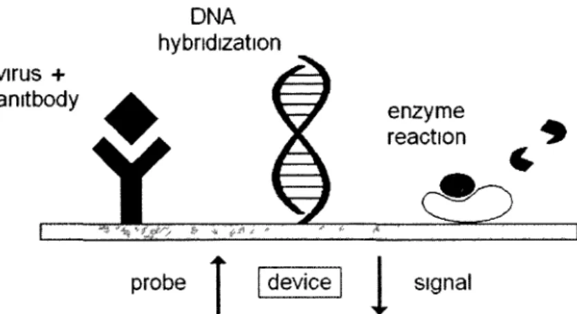
Figure 1.1 is a schematic diagram illustrating the fundamental biosensing concept. Shown are three common examples based on differentiated means of biochemical recognition.
DNA hybridization virus +
anitbody enzyme
reaction ^
probe I | device | signal
Figure 1.1. Generalization of biosensing concept. The immobilization of specific analyte results in a characteristic signal when the sensing device is subsequently probed. Three common mechanisms of biochemical recognition are shown.
Sensitivity is a critical issue for biosensors, especially those based on antibody-antigen coupling, the reason being that the binding affinity of an antibody is derived in large part from its proteomic structure [Prasad, 2003]. Therefore, if the functional conformation of surface-prepared antibodies becomes compromised, the sensing layer will operate less effectively. Biosensors based on DNA technology are particularly well-suited to illustrate the concept of specificity, which derives from the requirement for base-pair sequence matching between target and probe strands [Zhai et al, 1997]. In order to illustrate the concept of transduction, a useful example is the glucose sensor, which is based on the principle of enzyme reaction. The input components glucose + O2 are converted to gluconic acid + H2O2 by the enzymatic catalyst plumse nviHa^p Subsequently, the H2O2 product h reduced at the sensor cathode resulting in a measured current, or similarly, the consumption of O2 is monitored. This transduction mechanism is referred to as amperometric. Amperometric devices based on enzymatic reactions were some of the first biosensors developed, initially reported several decades ago [Clark and Lyons, 1962].
Since then, although many attractive approaches to biosensing have been proposed in the academic and patent literature, commercial success has been daunted by cost and challenged by increases in the effectiveness of high-throughput analytical chemistry [Luong et al, 2008]. Today, the biosensor market remains largely (~ 85%) comprised of glucose sensor variants
[Newman and Turner, 2005]. This level of market dominance is a consequence of the relative maturity of this technology, its perpetual need as a therapeutic diagnostic, and the increasing prevalence of lifestyle associated type 2 diabetes. Developing specialty applications hold the promise of sensing tools for point-of-care medical diagnostics, immunoassay and genomics research, defence and environmental monitoring, and use in the food, drug and agriculture industries. These opportunities have spawned a boom in biosensor research within the past several decades, inviting contributions from several facets of biochemistry, physics, engineering, and more recently, the field of nanoscaled materials.
The classification of biosensors is usually made according to the transduction mechanism through which they operate. Some common examples are categorized in Table 1.1.
TABLE 1.1. General classifications of biosensors based on transduction mechanism. biosensor classification transduction mechanism technology examples electrochemical optical A optical B thermometric stress / mass increase semiconductor A semiconductor B amperometric / voltammetric spectroscopic mode dispersion heat of reaction piezoresistive / piezoelectric channel conductance photoluminescence in vivo electrode FRET/SERS SPR / waveguide enzyme calorimetry MEMS /QCM BioFET
near-surface quantum dot FRET - fluorescence resonance energy transfer; SERS - surface enhanced Raman scattering; SPR - surface plasmon resonance; MEMS - micro-electro-mechanical systems;
QCM - quartz crystal microbalance; BioFET - biosensing field-effect transistor
Although not an exhai'sti^e list, Table !.! serves to locate a TL-'udbcu biosensing device within the general landscape of sensor technology. Technological examples of the various transduction mechanisms are included in column 3. For instance, electrochemical sensors, in addition to their ubiquitous role in glucose detection, have broad reaching clinical relevance in the areas of in vivo blood gas and electrolyte monitoring, despite ongoing biocompatibility issues [Shin and Schoenfisch, 2006]. Optical spectroscopic detection approaches often utilize donor/acceptor energy transfer processes in order to take advantage of proximity modulated fluorescence, made evident, e.g., in the DNA molecular beacon concept [Ortiz et ai, 1998]. The intensity of fluorescence labels is also dependent on the local environment, which can be
affected by binding-induced conformational changes in the proteins to which the labels are attached [Watkins and Bright, 1998]. DNA microarray or 'gene-chip' technology provides an example of multiplexed spectroscopic analysis that has reached commercial viability. For example, the products offered by Affymetrix Inc. incorporate probe-target DNA hybridization detected by fluorescent labeling, with probes arranged in a two-dimensional (2D) array on a quartz substrate allowing a high degree of parallel analysis. Optical mode dispersive technologies, such as surface plasmon resonance imaging and waveguide arrays, are expected to become competitive once their potential capacity for multiplexed analysis can be leveraged. In a recent example of this type, silicon photonic wire waveguide technology was demonstrated in a cascaded configuration that uses only one optical input to service a multiplexed array of spiral Mach-Zender interferometers, each of which may be functionalized with a different recognition element for in situ and parallel processing within a single microfluidic channel [Densmore et al., 2009]. Thermometric sensors are based on calorimetry and are usually developed around an enzyme catalyst. These devices will advance towards miniaturization with the realization of multi-analyte, temperature stabilized microfluidic systems [Ramanathan and Danielsson, 2001]. Sensors that exploit mechanical properties such as differential stress or mass increases utilize the resulting change in substrate conductance or resonant frequency in order to render the detection signal. Canti levered MEMS [Raiteri et al., 2001], or piezoelectric QCMs [Collings and Caruso, 1997], are common examples of this type.
Discussion of the semiconductor-based varieties will be deferred until Section 1.3. For now it will suffice to categorize them as channel conductance or PL types. To reiterate, the latter approach is the hrnaH topic into which the present work fits. However, since both types substantially depend on the characteristics of the semiconductor interface with molecular sensing architectures, this work bears relevance to the conductance approach as well.
1.2 Surface Chemistry and Molecular Self-Assembly
Common among the biosensor classifications is the need to develop appropriate chemistries that can deliver the required functionality. Surface-based approaches are especially challenging in this regard because of the orientational constraint that is imposed on the molecular order by the semi-infinite plane. Factors like surface coverage, surface
hydrophobicity, non-specific binding, and the presentation of conformational ly correct functional sites at the required density are practical considerations that, ultimately, must be addressed. Molecular self-assembly is a ubiquitous and enabling technology that has driven much of the advancement is this critical area [Wink et ai, 1997]. Self-assembly processes derive spontaneous molecular order from weak (non-covalent) molecular interactions, such as van der Waals forces or hydrogen bonding; the self-assembled system eventually reaches thermodynamic equilibrium with a structure that is uniquely determined by its size, geometry and number of constituent molecules [Halley and Winkler, 2008]. Note that the equilibrium condition limits the continued aggregation of molecular material. The self-assembly process is also reversible. Two familiar examples of self-assembly found in nature are the phospholipid bilayers that comprise cell membranes and the double-helix arrangement of nucleotides in DNA. In the cell membrane, the hydrophobic effect drives the assembly mechanism, whereas in DNA, the structure is formed by hydrogen bonding. From a practical standpoint, it is the spontaneous nature of self-assembly that makes it attractive for bottom-up approaches to nanotechnology. Self-assembly may even proceed beyond local ordering to incorporate the organization of building blocks into supramolecular assemblies. For example, advanced polyhedral structures, ranging in size from 1 0 - 4 0 nm, can be fabricated utilizing hierarchical DNA nanoassembly techniques [He et ai, 2008]. A relatively new approach to analyte binding similarly exploits the spontaneous organization of nucleic acid sequences into three-dimensional structures. Known as aptamers, these oligonucleotides, which are developed in an iterative selection and amplification process, have high-affinity for targeted molecules based on their conformation, with binding strength derived from hydrogen bonds or
n h o s n h a f p p r o u n assnrifltintr; T M r r i o w n ot nl IQQS1 ImmnhilivpH in KirvcpncirwT onnlir-Qtinnc
for example [Kleinjung et ai, 1998], aptamers have the advantage of smaller size and better conformational stability with respect to antibody ligands, factors which, respectfully, decrease steric hindrance and improve surface functionality.
For surface-based biosensing applications, an effective approach is to leverage the intermolecular attraction of linear alkanes («-alkanes), the general class of which is described by the formula [R' (CH2),, RJ], where the RIJ are individual functional groups. Some common examples of functional alkane terminations are: SH (thiol), NH2 (amine), OH (hydroxyl), COOH (carboxylic acid), or C-PO(OH)2 (phosphonic acid). Long-chain n-alkanes are
particularly useful for biosensing applications as their intermolecular affinity is strong enough that they spontaneously form two-dimensional pseudo-crystalline monolayers, which satisfies the orientational constraint imposed by the surface. An analogous system for the study of the resulting molecular order is the Langmuir monolayer, which is formed by amphiphilic lipids on liquid surfaces [Kaganer et al, 1999]. If one of the terminal functional groups is suitably reactive, then the monolayer can be covalently attached to the surface forming a SAM. Chemisorption is the term used to differentiate covalently bonded surface adsorption from physisorption, which is based on weaker physical attraction. The chemisorption approach to monolayer self-assembly has been adopted in a number of material systems. The model example is that of [HS(CH2)„CH3] alkanethiol SAMs formed on the Au(l 11) crystallographic surface. In this case, thiol functional groups react with the Au surface atoms to form covalent S-Au bonds. The resulting organization of the SAM is highly ordered, with an alkane chain tilt orientation of about 25°-30° from vertical and a surface cell, in Woods notation, of
(s!3xj3)R30° with respect to the Au(l 11) lattice [Dubois and Nuzzo, 1992].
When the terminal groups of the SAM are also of the functional type, they can be used to interact directly with specific analyte in a detection scheme, or can be used to anchor higher order recognition elements to the surface. Two illustrative examples of the use of SAMs in biosensor architectures are shown below in Figures 1.2 and 1.3.
dopamine
carboxylic acid terminated SAM
I Aul
Figure 1.2. COOH-terminated alkanethiol SAM used for dopamine recognition via electrostatic discrimination on a gold voltammetric electrode. Acid dissociation constants determine the charged molar fractions. Hydrogen bonds may also appear.
ascorbic acid
In Figure 1.2, a carboxylic acid terminated alkanethiol SAM discriminates dopamine, an important neurotransmitter, from ascorbic acid present in the extracellular fluid of the central nervous system [Malem and Mandler, 1993]. Due to their respective acid dissociation constants, the carboxylic acid and ascorbic acid are negatively charged at neutral pH, whereas dopamine carries a positive charge. However, both dopamine and ascorbic acid are electrochemically oxidized at voltammetric electrodes significantly impairing detection specificity. The electrostatic interactions discriminate by selectively presenting the dopamine to the SAM functionalized surface at lower oxidation potentials. In addition, Figure 1.2 depicts that hydrogen bonding between the amine and carboxylic functional groups is a possible second mode of affinity [Chai and Cahen, 2002].
In an example of higher order functionalization, alkanethiol-based SAMs incorporating a biotin functional group are commonly used in order to couple with streptavidin proteins. Subsequently, this protein may be used as a bridge to other biotinylated species, such as a biotinylated antibody or DNA probe strand, given there are four biotin-available binding sites per streptavidin. In practice, a mixed monolayer is often formed using the two molecule types shown in Figure 1.3.
HS v \ A A A / ^ hydroxyl-terminated alkanethiol
O S_
H S S / S / V / V N M ' * V ° V 'S 0' ^ ' ^ V S A A N H biotinylated polyether alkanethiol
N H O N H " ^0
Figure 1.3. OH-terminated and biotinylated polyether thiols form mixed molecule SAMs for streptavidin immobilization. OH-thiols provide spacing and hydrophilic repulsion against the polyether (C-0-C)„ sections resulting in biotin stand-off and reduced steric hindrance. In this scheme, the shorter (alkane only) molecules act to space out the biotin coupling sites and their hydroxyl termination provides repulsive forces against the hydrophilic polyether part of the longer biotinylated molecule. These properties serve to provide an effective stand-off for the biotin functional group so they may couple to streptavidin with less steric hindrance [Mittler-Neher et ai, 1995]. Surface stand-off also helps avoid protein denaturation, i.e., the loss of reactivity stemming from a loss of functional conformation. In the proposed PL biosensor, an alkanethiol-based SAM approach to the functional surface chemistry has been adopted. For example, it was recently demonstrated that influenza A virus could be
specifically immobilized on the GaAs(OOl) surface using biotinylated polyethylene glycol
alkanethiols in a mixed monolayer approach [Duplan et al, 2009].
In addition to the list of practical considerations stated earlier, a primary criterion for
effective performance is that the SAMs be compatible with the transduction mechanism. In
fact, SAMs have the potential to play an integral role in the transduction mechanism itself.
Consequently, it is important to understand their fundamental physical properties. It is only
through detailed characterization that such foundational knowledge can be obtained and that
new insights may be brought to bear on applications development. This knowledge is required
in order to understand the limitations of a particular approach, or to help validate
computational models, which ultimately supports more advanced system analysis. In order to
develop a specific framework within which the present research may be developed, this
investigation focuses on the first order interface, i.e., the physical properties of alkanethiol
SAMs and the nature of their coupling to the GaAs(OOl) surface. Results from more advanced
surface chemistry will be discussed only briefly.
Not only do SAMs have relevance within the biosensing context, they have also been
adopted for use in the investigation of junction-based molecular electronic applications. In
particular, the electronic band alignment and transport characteristics of alkane SAMs are of
fundamental importance, which are often studied using metal-molecule-semiconductor
(MMS) heterostructures in which the SAMs comprise the insulating barrier. For example,
analysis of current-voltage data indicates that tunneling dominates the transport characteristics
at high forward biases [Lodha and Janes, 2006; Nesher et al., 2006]. Some general comments
on the relevance of the present work to the field of molecular electronics will also be made.
1.3 S e m i c o n d u c t o r - b a s e d Biosensing
1.3.1 Channel Conductance Methods
Semiconductor-based sensing devices in the electronic domain are typically designed
around the field-effect transistor. Often referred to as BioFETs, or ChemFETs, they derive
from the ion-selective FET (ISFET), first developed by Bergveld [Bergveld, 1970]. The
operating principle of an ISFET differs little from that of the standard MOSFET, e.g., the
gate-insulated, n-channel type, where the gate potential controls the drain current (/„), i.e.,
the channel conductance, by varying the charge density in an inversion region below the gate.
Above the threshold voltage (Vlh) and below saturation, the FET device is ohmic and responds
linearly to the gate potential [Streetman and Banerjee, 1999]. In the 1SFET, the metal gate is replaced with an electrolytic analyte solution, into which a reference electrode is submerged and is held at some fixed gate potential (V(i) with respect to the semiconductor ground.
Protonation of OH-groups on the surface of the gate insulator, typically the semiconductor oxide, changes the surface potential {y/) at the insulator-electrolyte interface in response to solution pH [Bergveld, 2003a]. The change in surface potential shifts the flat-band voltage, which is the contact potential between the semiconductor and reference electrode in the electrolyte. The ISFET threshold voltage, which depends on the flat-band voltage, is thus directly controlled by the surface potential. Since the gate voltage is held constant, a second means to linearly control the drain current is obtained. The governing ISFET parameters are summarized in the following,
h> x [Vc, ~ V,Hi¥)] V,y + constant (1.1)
where VD is the applied drain voltage. In practice, a feedback circuit can be used to maintain a
constant drain current by modulating the gate voltage, which then serves as the sensor output [Barbara et ai, 1992], and maintains the device within the ohmic regime.
In the BioFET or ChemFET, the surface of the gate insulator is functionalized with a biologically or chemically selective agent, usually imbedded in a semi-permeable membrane. The difference with respect to the ISFET is that the surface potential (i.e., threshold voltage) offset at the gate is now effected by means of pH variation in the sensing layer produced by localized reactions. For illustration purposes, consider the urea sensor, which operates using the following enzym?tjc reaction mediated by membrane immobilized uit,a»c,
urease
(NH2 )2 CO + 3H20 -> IN; + OH~ + HCO~ (1.2)
producing ammonia, hydroxyl and carboxyl ions. In an ISFET sensor, the relative dissociation of these ionic species determines the pH, and consequently, the charge density at the sensing interface varies [Bergveld, 2003b]. In the actual device, the differential voltage with respect to a reference arm FET can be used in a feedback mechanism to maintain a constant pH through the use of coulombic compensation [van der Schoot and Bergveld, 1987]. The detailed
operational considerations of BioFETs designed for the sensing of charged macro-biomolecules in electrolyte solutions has also been reviewed [Landheer et al, 2005].
Another method of sensing that utilizes FET junctions contrasts with the ion-selective approach in that it is net charge neutral and requires no referencing electrode. Frequently referred to as the Molecular Controlled Semiconductor Resistor (MOCSER), these devices exploit dipole moment variations in a molecular layer prepared on, e.g., the gate insulator [Rudich et al, 2000] or, a back-gated semiconductor channel layer [He et al, 2006]. GaAs-based high electron mobility transistor (HEMT) designs have been also been demonstrated [Wu et al, 2001], as illustrated in Figure 1.4. In these designs, differences in the source-drain current are realized by adsorbate-induced effects on the channel layer potential.
molecular sensing layer n-GaAs channel layer —. <k/jXkJ>£> ^ s - ^ s ^ GaAs
Figure 1.4. HEMT design MOCSER with porphyrin-based SAM used for the detection of nitric oxide in physiological aqueous solutions.
Transduction arises from dipole moment variations of the surface potential, in contrast to the monopole derived field-effect of the ISFET. A MOCSER response can be initiated through the ordered adsorption of polar molecules [He et al, 2006; Song and Lu, 2006], or the induction of dipole moments in polarizable SAMs [Wu et al, 2001]. However, the actual mechanism of transduction has several facets to consider [Natan et al, 2007]. One explanation refers to a Cooperative Molecular Field Effect (COMFE) in which it is suggested that charge transfer car, be effected between an ordered 2D nioi^umi iayci <uiu its subsume [Cahen et al, 2005]. This charge transfer is thought to result from the establishment of a new surface equilibrium upon the adsorption of specific analyte. Central to the COMFE argument is that the resulting charge transfer minimizes dipole-dipole repulsive forces that act in an ordered 2D molecular array. For example, the COMFE was used to explain current variations through a Si-based MOCSER device, reported in work by Rudich et al [Rudich et al, 2000], where the device was prepared with (methyl-terminated) octadecyl trichlorosilane SAMs and observed under various environmental partial pressures of O2 and HiO. The current variations
were opposite in sign, and were suggested by Cahen et al. to be linked to a COMFE reversal of dipole moments in the SAM following the physical adsorption of these two species.
Clearly, the surface potential plays an important role in the transduction mechanism of FET-based sensors. This statement generalizes to include the PL-based sensors, as shall become clear in the following section. In this thesis, surface and interface dipoles associated with alkanethiol SAMs have specific implications in terms of the electro-optic response of the GaAs surface. Before proceeding to a more detailed discussion of the research objectives, however, the PL-based approach to sensing must also be given a brief introduction.
1.3.2 Photoluminescence Methods
In practical terms, PL describes the process of radiative recombination in semiconductors following the absorption of supra band-gap energy photons. Optically excited conduction band electrons and valence band holes, once thermalized to their respective band edges, spontaneously transition to the ground state releasing photons characteristic of the band-gap energy. In direct band-gap material, the Bloch wavevector is conserved without phonon-assistance and, therefore, the radiative transition is more efficient. By the same token, the absorption of optical excitation is also made efficient, and consequently, electron-hole pair generation occurs within a thin near-surface layer typically less than a few hundred nanometers thick. Since the optical absorption length is much less than the diffusion length for minority carriers, they reach the surface within their radiative decay lifetime and return to the ground state through trap-assisted non-radiative transitions, as illustrated in Figure 1.5.
i ii • ii i E9
hv^
4 CB
hv
0 i II o II i VB • * o « * • • ( ) * » • • • • • * » o * » • • • • • • • • • • • • • • • • • • • • • • • • • • • • • • • • • • • • • • • • • • • •excitation non-radiative radiative
Figure 1.5. Recombination processes in GaAs. Optical excitation generates conduction band (CB) electrons, which relax to the CB-edge by phonon release (|||*|||). Subsequent non-radiative relaxations result in carrier pair annihilation at the trap level (E,) by hole and electron capture. Radiative processes involve direct transitions to the valence band (VB) releasing photons with energy (/iv2 < ItVi) corresponding to the band-gap (Eg).
Consequently, the PL intensity can be highly sensitive to surface conditions that dictate the
parameters affecting the rate of surface recombination. Among these parameters list the
number density and energy positions of the defect states though which the non-radiative
transitions occur. Their type (donor/acceptor) and occupation are also important, as are other
surface potential factors that may alter the near-surface band structure. The overall
recombination rate is inversely proportional to the minority carrier lifetime ( r ) , which
consists of radiative and non-radiative terms in the reciprocal sum [Yacobi, 2003],
I-1.-L (1.3)
T X T
r nr
Two convenient simplifications may be introduced: i) the radiative term is considered an
intrinsic bulk quantity, and ii) the non-radiative term is assumed to be dominated by surface
conditions. The rates associated with these lifetime terms may be approximated by,
r
r= r;
1*/?(*„ + An) = 0n (1.4)
r„=T;
lr=cr
pv^
pN, (1.5)
for n-doped material specifically. Similar equations for p-doped material may be written
directly. In Equation 1.4, n
ais the equilibrium majority carrier (electron) concentration, An is
the photo-generated excess concentration due to electron-hole pair generation (An = Ap),
and p is the radiative rate constant for GaAs, applicable under non-degenerate injection
[Lambert et ai, 1990]. Equation 1.5 is based on Shockley-Reed-Hall recombination theory
[Shockley and Read, 1952; Hall, 1952], simplified for the limiting conditions of low level
photo-injection and defect energy positions located near mid-gap (i.e., deep levels), where a
is the minority carrier capture cross-section, v
lh pis the minority carrier thermal velocity, and
N, is the trap density (see Chapter 2). The relative yield of PL intensity can be quantified in
which is, in essence, the governing equation behind the transduction mechanism in an intensity-based PL sensor. Specifically, adsorbate induced changes to either the radiative or non-radiative rate will alter the relative PL yield, which serves as the appropriate metric.
In accordance with the assumption that surface recombination dominates the non-radiative rate, Equation 1.5 may be explicitly defined as a surface quantity referred to as the surface recombination velocity (SRV). Variation of the SRV results in changes to the PL yield. For example, adsorbate-induced reductions of either crp or N, lead to decreases in the
non-radiative rate and, consequently, to the enhancement of ypl . In addition to SRV
moderated effects, the depth-integrated radiative emission may be controlled via surface conditions. For example, the near-surface electric field associated with the depletion region typical of n-type surfaces tends to separate photo-generated carriers resulting in a so-called PL 'dead-layer' where the radiative rate is significantly decreased [Wittry, 1967]. Consequently, adsorbate-induced modifications of the depletion region directly affect the PL yield when the depth of the dead-layer region is changed. Both the SRV and dead-layer mechanisms are important to the operation of a PL-based sensor designed on the single-crystal wafer. A schematic illustration of the near-surface band-bending typical of most semiconductor surfaces is provided in Figure 1.6 (top), and includes the associated charge densities (bottom) showing the surface trapped charge and space charge that characterize the depletion region.
r \ <E
q®
sb<{ V —»-eee
'-<|[
^
E ^TTrrrr-r—^_J v?
flat-band < © # © qN + + + + + + + + + + + + •* EFigure 1.6. Near-surface band structure of n-type GaAs in depletion. Symbols: space charge density (qN^), space charge region (SCR), depletion depth ( zd) , surface
trapped charge (-), ionized donors (+), surface charge density (Qs s), Fermi level
energy (FL), conduction/valence band-edges (CBE/VBE), surface barrier height (q<£>sh),
built-in electric Held ( ' i ) and energy density of surface acceptor states (£)„)• Photo-generated excess minority carriers ( ® ) are driven into the SCR by drift and diffusion processes contributing to the non-radiative SRV and a reduction of the radiative recombination rate.
Historically, PL-based sensors have operated using transducer films or direct adsorption,
and have been extended to incorporate a wide variety of gas-sensor designs by the group of
A.B. Ellis, particularly [Seker et ai, 2000]. Transducer films are a general class of analyte
sensitive surface treatments designed to affect the necessary surface conditions responsible for
PL intensity variation. An early example was based on the PL response of a n-doped
Pd-CdS
xSei.
xSchottky diode to adsorbed H2 [Carpenter et ai, 1985]. Hydrogen gas is known
to lower the work function of Pd, which, at the n-type junction, establishes a new thermal
equilibrium (Fermi level alignment) by decreasing the semiconductor band-bending. By virtue
of the dead-layer model, this decrease in the barrier height corresponded to a PL increase. A
later example of the transducer type exploited the gas-induced oxidation of a silo-ferrocene
functionalized n-GaAs substrate [Van Ryswyk and Ellis, 1986]. Iodine or bromine in a
nitrogen gas mixture was used to increase the oxidation state of the ferrocene, resulting in PL
quenching, while exposure to hydrazine gas (N2H4) reversed the effect, returning the PL to its
original intensity. The operation of this sensor was also attributed to the dead-layer model.
In contrast to the transducer film type, direct adsorption sensing refers to the case where
analyte adsorbs directly on the semiconductor surface via physical attraction (physisorption),
which can be characterized by Langmuir kinetics. In this mode, both PL enhancement and
quenching have been attributed to the formation of surface-adsorbate complexes; specifically,
those derived from Lewis acid-base chemistry, commonly referred to as adducts. PL
enhancement is correlated to the basicity of adduct-forming adsorbates, while acidity
correlates with quenching [Luebker et ai, 1991]. For example, the lone-pair electron donating
potential of Lewis bases, such as the class of gaseous amines, has been suggested to account
for PL enhancement in the dead-iayer modei [Meyer et ai, J988]. In this case, surface trapped
electrons are thought to be displaced, resulting in a contraction of the depletion region.
However, SRV related phenomena, such as an increase in the minority carrier lifetime, have
also been measured depending on the surface preparation [Leung et ai, 1990].
In summary, the PL method of semiconductor surface-based sensing relies on
analyte-induced variation of the conditions responsible for the overall surface electronic
profile. Specifically, variation of the surface potential, including static charge, dipolar or
surface complex related effects, can modify the number density, energy distribution,
occupation and/or trapping efficiency of surface state defects. A change in these parameters
results in PL yield enhancement or quenching by virtue of the (non-radiative) SRV and
(radiative) dead-layer mechanisms. Ideally, designing for the successful operation of a PL
biosensor requires a detailed understanding of these mechanisms, the limitations they impose,
and how to address them via changes in the surface potential in order to realize a useful
dynamic range in a controlled manner. Isolating the effects of these two contributing factors is
important to this understanding and factors significantly into the present research.
1.4 Motivations and Research Objectives
In the preceding discussions, the importance of surface chemistry and molecular
self-assembly to the operation of biosensors was introduced and the surface potential was
highlighted as a critical design parameter in semiconductor-based systems with particular
emphasis on the PL sensing method. In this section, questions relevant to the incorporation of
molecular self-assembly within the PL approach are defined in order to establish the research
objectives. The surface potential and its associated electro-optic effects specific to the
alkanethiol SAM interface with the GaAs(OOl) surface comprise the overall context. This
material system represents the prototypical SAM-semiconductor interface and was chosen, in
part, in order to leverage the body of literature that reports on it from the perspective of the
fundamental material science. Although this system does not incorporate a more sophisticated
biosensing architecture, it represents a possible first order molecular architecture in such a
design, and further knowledge of it will inform the development process. Consequently, the
central hypothesis of this thesis questions how the electro-optic properties of the SAM-GaAs
interface derives from its physical structure, and what significance is there for the biosensing
mechanisms. Accordingly, this work is categorized into the following three subsections.
1.4.1 Structural and Chemical Characterization
The first category relates to a characterization of the basic structural and chemical
parameters. These are important to verify before examining the more detailed electro-optic
data. For example, the process of SAM formation requires an etching step in order to remove
the native oxide. This promotes coupling of the reactive thiol group to the exposed crystal
face through covalent bonding. The resulting GaAs stoichiometry is important to an
understanding of the surface state, which has implications with respect to the surface barrier
height at the SAM-semiconductor interface. Evidence of physico-chemical signatures
characteristic of thiol chemisorption and molecular ordering of the SAM must also be verified. These speak to the overall structure, coverage and stability of the interface.
1.4.2 Electronic Properties of the SAM
The surface potential introduced to the GaAs interface following SAM formation is a fundamental electronic property with potential implications for the PL intensity via SAM interaction with the GaAs interface states. Therefore, knowledge of the surface potential must first be obtained. Since the SAM is charge neutral and consists of molecules retaining a permanent dipole moment, changes to the external work function are expected, i.e., changes to the vacuum level energy. In addition, the passivation of surface defect states may also be expected, which can, e.g., reduce the surface charge density and associated surface barrier height. This effect is quantified by changes in the surface Fermi level following SAM formation. Moreover, considering the SAM phase as distinct and in view of such theories as the COMFE, it is expected that the electronic properties of the SAM will be altered from that representative of the source material in bulk molecular form. If such a reconfiguration is manifested, it is proposed this will be reflected in changes to the optical constants of the SAM in a manner consistent with its pseudo-crystalline molecular structure.
1.4.3 Electro-Optic Response of the GaAs Interface
Following SAM formation, the passivation of PL quenching surface oxides will be apparent from the stoichiometry of the GaAs surface. Quantification of the surface Fermi level change as a result of SAM formation will be a further step towards understanding the PL response at the SAM-GaAs interface. However, one of the shortcomings of the dead-layer model U that it assumes the photo-injected electron density docs not perturb the balance of charge in the equilibrium picture that it implies. As an interfacial layer in the proposed biosensor architecture, how the surface barrier of thiol-passivated GaAs reacts under steady-state photo-injection needs to be investigated. More specifically, an understanding of both the dead-layer and SRV mechanisms is required. It is proposed that thiol-induced effects will influence the near-surface band structure in a manner that is consequential with respect to sensor design. Decoupling of the SRV into its constituent factors, i.e., the capture cross-section and surface trap density, is accomplished using both experimental and modeling approaches in order to provide the necessary insight.
1.5 Structure of the Thesis
In this section, an outline of the overall document plan is presented as follows. Chapter 2 is comprised of the detailed background, in terms of both the relevant literature and theory, which informs the discussion in subsequent chapters and provides the necessary justification of the topics selected. This chapter is divided into the following parts according to the various experimental and numerical methods employed in this work:
i) X-ray Photoelectron Spectroscopy (XPS), including angle-resolved (ARXPS) techniques, and methods used to obtain the surface Fermi level and work function, ii) Infrared (IR) Spectroscopy specific to the molecular ordering, SAM orientation and
principal components of the SAM optical constants,
iii) Kevin Probe methods including the Surface Photovoltage (SPV) technique, which relate to the work function and the steady-state electronic band structure respectively, iv) PL methods and its quantification in terms of the radiative yield enhancement, surface
recombination velocity, and power dependence.
Chapter 3 discusses the compositional stoichiometry and structural morphology at the SAM-GaAs interface, as determined by XPS, and largely consists of unpublished results. In addition, details on the method of sample preparation are provided, which are common to the work in the remaining chapters. The ARXPS technique figures prominently with respect to several aspects of the analysis.
Chapter 4 reports on the IR spectroscopy of the SAM revealing evidence for enhanced vibrational properties unique to the SAM phase [Marshall et al, 2009a], from which the optical constants of the SAM are derived [Marshall et al, 2009b]. In addition, ex situ IR spectroscopy measurements of the SAM formation dynamics help turther the understanding of the self-assembly process [Kim et al., 2009]. Also, a demonstration of second order surface functionalization is briefly described, specifically, the covalent coupling of biotin to amine-terminated alkanethiol SAMs [Dubowski et al, 2010].
The equilibrium energy levels associated with the SAM-GaAs interface are investigated in Chapter 5. For example, the work function change resulting from the SAM's dipole contribution is quantified using XPS and Kelvin Probe methods. Interestingly, the work function change is observed to correlate with the IR absorbance according to the variation in SAM molecular length [Marshall et al., 2009b]. This correlation provides further insight into