HAL Id: hal-02005757
https://hal.archives-ouvertes.fr/hal-02005757
Submitted on 12 Nov 2020HAL is a multi-disciplinary open access archive for the deposit and dissemination of sci-entific research documents, whether they are pub-lished or not. The documents may come from teaching and research institutions in France or abroad, or from public or private research centers.
L’archive ouverte pluridisciplinaire HAL, est destinée au dépôt et à la diffusion de documents scientifiques de niveau recherche, publiés ou non, émanant des établissements d’enseignement et de recherche français ou étrangers, des laboratoires publics ou privés.
Sensitivity analysis of the electrostatic interaction
between the atomic force microscopy probe and a thin
dielectric film with 3D-localized charge cloud
Menouar Azib, Fulbert Baudoin, Nicolas Binaud, Christina Villeneuve-Faure,
G. Teyssedre, Florian Bugarin, Stéphane Segonds
To cite this version:
Menouar Azib, Fulbert Baudoin, Nicolas Binaud, Christina Villeneuve-Faure, G. Teyssedre, et al.. Sensitivity analysis of the electrostatic interaction between the atomic force microscopy probe and a thin dielectric film with 3D-localized charge cloud. Journal of Applied Physics, American Institute of Physics, 2019, 125 (4), pp.045305. �10.1063/1.5060655�. �hal-02005757�
1
Sensitivity analysis of the electrostatic interaction between the
Atomic Force Microscopy probe and a thin dielectric film
with 3D-localized charge cloud
M Azib1,2, F Baudoin1, N Binaud2, C Villeneuve-Faure1, G Teyssedre1, F Bugarin2
and S Segonds2
1 LAPLACE, University of Toulouse, CNRS, INPT, UPS, 118 route de Narbonne, F-31062
Toulouse, France
2 Paul Sabatier University; ICA (Clement Ader Institute), 3 Rue Caroline Aigle, F-31400
Toulouse, France
Abstract. Recent experimental studies have demonstrated that Electrostatic Force Distance Curve (EFDC) can be used for space charge probing in thin dielectric layers. Experiments highlight that this method seems to be sensitive to charge localization. However, the relative contributions of charge distribution parameters (density, lateral/in-depth spreading) remain unknown. The aim of this paper is to determine the contribution of each charge distribution parameters to EFDC. To reach this aim, we have developed an electrostatic and an electromechanical model to simulate EFDC over a charge cloud trapped in a thin dielectric layer. Hence, the EFDC sensitivity to charge localization could be investigated through the shape parameters of the charge cloud and by extracting the respective contributions from the Atomic Force Microscopy (AFM) tip and the cantilever.
I. Introduction
Atomic Force Microscopy (AFM) [1] appears as a very useful and versatile instrument for imaging surfaces and for characterizing materials properties at nanoscale such as electrostatic properties of thin layer materials [2]. Associated with the electrostatic characterization of surfaces, most of the theoretical studies on electrical modes derived from AFM have been focused on the quantitative estimation of the electrostatic force between an AFM probe and a sample. These studies are based on 3D or 2D analytical models [3, 4] or Finite Element Model (FEM) [5-6]. The main issue for modelling the electrostatic interactions in AFM is its complexity with notably multiscale objects. Therefore some simplified model systems are used to describe the complex AFM setup. In general, the sample is
2
assumed flat, the cantilever is not taken into account or approximated by simple disk, and some geometric entities are assumed as representative of the AFM "tip": a simple charge [7], a sphere [8,9] or a cone [10], are the most used shapes. In some cases more sophisticated "tips" are proposed such as a spherical cap connected to a tip cone [4] or rectangular cap connected to a tetrahedron [5]. The latter is the closest to the real tip and the simulation results have been compared to the experimental results. The electrostatic force is essential to interpret results provided by techniques derived from AFM such as Kelvin Potential Force Microscopy (KPFM) [11] or Electrostatic Force Microscopy (EFM) [12] and estimating electrical parameters such as the relative permittivity [13-15], the “real” surface potential [16] or an image of charge density through the surface potential [17-21]. Concerning charge density determination, these techniques have been limited by their lack of in-depth sensitivity, i.e. it failed to determine precisely the spatial distribution of the charges in thin dielectric. Indeed, to determine charge density from KPFM measurement, hypothesis about charge localization in volume is needed. Previously, charges were considered either localized on the surface [22] or homogeneously distributed in the volume [23]. Knowing charge distribution in the volume is mandatory for a better understanding of charge transport and trapping phenomena in thin dielectric films and at metal/dielectric interface. This is the reason why the Electrostatic Force Distance Curve (EFDC) [24, 25] is investigated as a new tool to probe in 3D the charges in thin dielectrics. Preliminary experimental results show that the EFDC seems to be sensitive to the location of the charge in 3D [24, 25], or to electrostatic potential localization [26]. However, the relative contribution of charge distribution (density, lateral/in-depth spreading) is unknown and need to be identified to point out EFDC ability to determine 3D charge distribution.
In previous work [27], we proposed a numerical approach by developing a finite element model which permits to compute EFDC accurately over an embedded electrode. This model provides the complete description of the experiments and enabled us to analyse the contributions from the cantilever and from the tetrahedron tip.
The objective of this paper is to study EFDC sensitivity to charges localization in thin dielectric by FEM. Numerical simulation is implemented to estimate the electrostatic force exerted on the AFM probe induced by a half-ellipsoid charge distribution. The sensitivity of the EFDC shape to charge localization is investigated for the charge cloud parameters as lateral radius, depth and charge density. This paper is structured as follows. The section 2 is devoted to simulate EFDC with the electrostatic tip model. In section 3, the cantilever contribution to the tip model is detailed whereas the EFDC sensitivity to charge localization is analysed in section 4. Finally a conclusion is given with lines for forthcoming work.
II. Electrostatic tip model
The COMSOL Multiphysics [28] finite-element software has been used to simulate EFDC. The general equations of electrostatics have been applied for simulation.
3
A. Geometry description
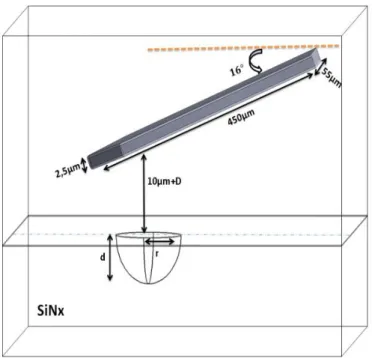
The geometry of the system (Figure 1) consists of a stationary tip positioned over an infinite dielectric layer (silicon nitride, SiNx) with a thickness of 500 nm and a relative permittivity =7.5. The tip has a tetrahedral shape ending with an apex (a half-sphere of radius R of 25 nm) [5].
The shape of charge cloud should be representative to that of charge injected by a biased AFM tip [25]. When charges are injected by a tip, the resulting surface potential map presents an axisymmetric shape respectively to the tip axis [29]. In addition, the radial field is higher at the surface than in the bulk. For these reasons, the trapped charge cloud into the dielectric layer is described as a half-ellipsoid cloud of uniform charge density , with a radius r and a depth d (see Fig. 1). Moreover, experimental results [25, 29] show that the lateral extension of injected charge is limited to 1-2 µm in the investigated SiNx or silicon oxynitride (SiONx) layers. So, in the following, radius r will range from 10 nm to 600 nm, the depth from 25 nm to 490 nm and the charge density from 1 104 C.m-3 to
5 104 C.m-3.
The tip is surrounded by an air box in contact with the dielectric surface whose dimensions are large enough to avoid edge effects. The cantilever is not represented here, because its contribution will be investigated in the next section using a 3D electromechanical model. So, in this section the study is focused on the computing of electrostatic force occurring between the AFM tip and the sample as function of their separating distance, D.
FIG 1. Description of the geometry used for tip-charge cloud EFDC modelling.
B. Equations
In this electrostatic model, the first step is to determine the electrostatic potential distribution in air box and in dielectric layer. The following step is to deduce the electrostatic force induced on the tip by the charge distribution stored in the dielectric layer. This requires the resolution of the Poisson’s equation (1) in the domain Ω, taking into account the boundary conditions on the interface Γ (see Figure 1). Γ is composed of three parts Γ0, Γ1 and Γ2. The problem is written as follows:
4
in (1)
on Γ0 and Γ1 (2)
0 on Γ2 (3)
where is the charge density, n is the vector normal to the surface and is the permittivity. The tip and the sample back side are set to the ground. To ensure no edge effects, no charge conditions are applied on the free boundaries Γ2 of the simulation box. In order to solve numerically the Poisson’s
equation in the domain Ω and to determine the electric field distribution E, the FEM has been applied for meshing the geometry. In that aim, the regions where the electrostatic interactions are very high (around the apex) need to be meshed finely and the ones representing weak interactions can be meshed more coarsely. Thus, mesh was refined and optimized close to the contact point between the air and the dielectric following the procedure presented in [27].
Figure 2 shows the electric potential V (Figure 2a) and electric field E (Figure 2b) distributions for the separation distance D of 100 nm and a charge cloud with the following characteristics d = 100 nm, r = 150 nm and = 2.5 104 C.m-3. As expected, the electric field is enhanced close to the tip apex and the
maximum strength (1.2x10⁸ V.m-1) is reached on the tip apex. The field exceeds 10% of the maximum
field on the tip apex only. Outside the apex, the electric field is lower. This result confirms that the electrostatic force is dominated by the contribution of the tip apex. The electric field intensification close to the dielectric surface leads to a situation where the electrostatic interactions are very high, particularly on the vertical direction.
(a) (b)
FIG 2. (a) Electrostatic potential V and (b) electric field E distribution computed using FEM and optimized meshing close to apex.
C. Electrostatic Force Distance Curve (EFDC)
The electrostatic force F acting on the tip surface was computed by the integration of the built-in Maxwell-stress-tensor, over all faces of the tip:
5
(5)
Figure 3 represents the corresponding electrostatic force distance curve computed for the same charge cloud as for Figures 2a and 2b.
0 50 100 150 200 -2.5 -2.0 -1.5 -1.0 -0.5 0.0 F ( n N ) D (nm)
FIG 3. The electrostatic force F vs distance D between tip and sample, computed in the range from 0 nm to 200 nm with a step of 4 nm. For charge cloud characteristics of d = 100 nm, r = 150 nm and = 2.5 104 C.m-3.
III. Cantilever contribution to EFDC
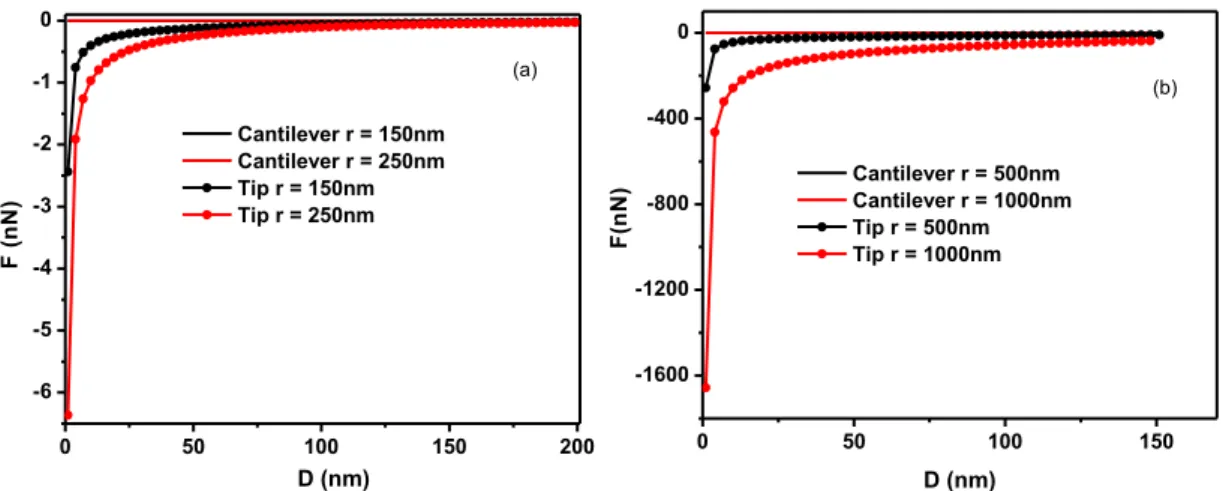
In this section we discuss the EFDC sensitivity to charges localization in 3D through the cantilever contribution. To extract the electrostatic force exerted on the cantilever by the charge cloud the general electromechanical equations are used [5]. FEM with optimized mesh (see Figure 4) was used as previously. The cantilever is modelled as an elastic beam fixed at the right end (mechanical fixed constraint) and tilted by the same angle as the axis of tip, i.e. α = 16°. The strategy consists in varying all the charge cloud parameters: the radius r, the density and the depth d; running simulations with each set of parameters, and then analysing the effect of these parameters variations on the EFDC. Thus, contribution of the cantilever is compared to the tip one.
6
FIG 4. Description of the geometry used for cantilever-dielectric electromechanical model.
Several parameters characterizing the cantilever beam geometry are used as summarized in Table 1: the thickness T, the width M, the length Lc and the spring constant k which are related by the expression:
(6)
where E is the Young’s modulus.
Table 1. Geometric parameters of the cantilever beam
Material Spring constant k (N.m-1) Thickness T (µm) Width M (µm) Length Lc (µm) Young's modulus E (GPa) Si/PtIr 0.36 2.5 55 450 165
Figure 5 shows the contribution of the cantilever computed using the electromechanical model compared to the tip contribution computed using the electrostatic model over the same spots of charges. The plots displayed respectively on Figures 5a and 5b were simulated for d = 100 nm, ρ = 2.5 104 C.m-3 and for d = 300 nm, ρ = 5.3 104 C.m-3. The red curves respectively on Figures 5a and
5b correspond to r = 250 nm and to r = 1000 nm, and the black curves respectively correspond to r = 150 nm and to r = 500 nm.
7 0 50 100 150 200 -6 -5 -4 -3 -2 -1 0 Cantilever r = 150nm Cantilever r = 250nm Tip r = 150nm Tip r = 250nm F ( n N ) D (nm) (a) 0 50 100 150 -1600 -1200 -800 -400 0 (b) F (n N ) D (nm) Cantilever r = 500nm Cantilever r = 1000nm Tip r = 500nm Tip r = 1000nm
FIG 5. Comparison between the tip contribution and the cantilever contribution for different charge cloud radius: (a) for d = 100 nm and ρ = 2.5 104 C.m-3, (b) for d = 300 nm and ρ = 5.3 104 C.m-3.
As it can be seen from the Figures 5a and 5b, the contribution of cantilever is negligible compared to the contribution of the tip and in addition the lever’s force is nearly independent from the distance D (in the investigated range). Indeed, the lever contribution for r = 250 nm or r = 150 nm is in the order of 10-8 nN while the tip contribution is in the order of nN (see Fig. 5(a)). The corresponding charge
quantity is in order of 10-16 C with the parameters of the charge cloud used. Figure 5b reveals that even
if we multiply the quantity of charge by a factor of 100, the contribution of the cantilever still remains negligible compared to the tip contribution. Indeed, the contribution of the lever is in the order of 10-4
nN, but the tip contribution is in the order of 103 nN; we still have the same ratio of about 10-8 between
the two contributions. Since the diameter of the charged area stayed much below the cantilever dimensions, the contribution of cantilever appears always negligible when localized charge cloud is investigated.
So, in the following only the tip was considered to investigate EFDC sensitivity to charge localization.
IV. EFDC sensitivity to charges localization through the tip contribution
In order to investigate the sensitivity of the electrostatic force distance curve (EFDC) to charge localization, the values of each charge parameters: the density ρ, the radius r and the depth d were modified successively, and then the impact of their variation on the force curve shape was determined. The force curve is well described empirically by the following equation [24]:
(7)
Where D is the tip-to-sample distance, is the force when the tip is far enough from the surface, is the maximum force at the contact point (D = 0), C characterizes the D-value of the sigmoid midpoint and p is a parameter describing the steepness of the curve. By considering different charge
8
configurations, an analysis of the maximum force ( ) and of the two parameters describing the curvature (C, p) is provided aiming at identifying their link to charge localization and density, and recognising the physical meaning of each parameter. Whatever charge cloud is considered, remains close to 0.
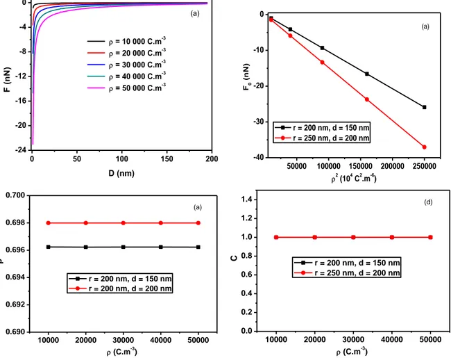
A. EFDC sensitivity to the charge density
Figure 6a compares the EFDC computed for different charge densities from 1 104 C.m-3 to 5 104
C.m-3 with a fixed radius to 250 nm and a fixed depth to 100 nm. Figure 6b shows clearly that
increases linearly with the square of charge density ( ). The slope of the vs. line depends on
charge cloud radius r and localization respect to the surface. Figures 6c and 6d show that the parameters of curvature (C, p) are constant with the charge density. Therefore, the charge density
influences only the maximum force and the constant value of the p parameter.
0 50 100 150 200 -24 -20 -16 -12 -8 -4 0 F ( n N ) D (nm) = 10 000 C.m-3 = 20 000 C.m-3 = 30 000 C.m-3 = 40 000 C.m-3 = 50 000 C.m-3 (a) 50000 100000 150000 200000 250000 -40 -30 -20 -10 0 (a) F0 ( n N ) 2 (104 C2.m-6) r = 200 nm, d = 150 nm r = 250 nm, d = 200 nm 10000 20000 30000 40000 50000 0.690 0.692 0.694 0.696 0.698 0.700 (a) r = 200 nm, d = 150 nm r = 200 nm, d = 200 nm p (C.m-3 ) 10000 20000 30000 40000 50000 0.0 0.2 0.4 0.6 0.8 1.0 1.2 1.4 (d) r = 200 nm, d = 150 nm r = 250 nm, d = 200 nm C (C.m-3 )
FIG 6. (a) Comparison of EFDC computed for different charge density (depth d and radius r were respectively fixed at 100 nm and 250 nm. Evolution of (b) maximum force , the parameters of the curvature parameters (c)
9
As the maximum force varies linearly with ( ) we can write that with is
a reference density. Since the parameters of the curvature are independent from the charge density then the electrostatic force F is represented only by in this case, therefore we can finally write:
(8)
For constant dimensions of the charge cloud the maximum force depends linearly on the square of charge density which means a linear dependency of the maximum force with the square of the total charge quantity Q: with the ellipsoid shape taken here, the mathematical relation which links the quantity of charge Q to charge parameters is described by the following equation:
(9)
B. EFDC sensitivity to the lateral spreading of charges r
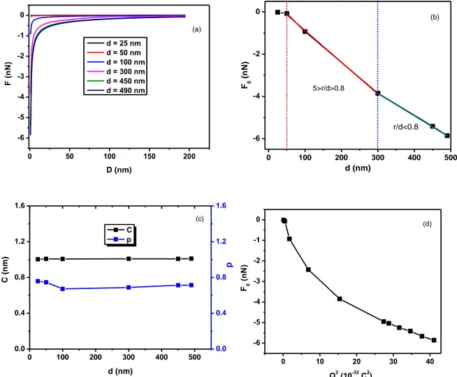
Numerical simulations of EFDC as a function of the charge cloud radius r (ranging from 10 nm to 600 nm) are presented on Figure 7a (depth d and density ρ are fixed respectively to 100 nm and to 1 104
C.m-3). Figures 7b represents the evolution of maximum force F0 as function of charge cloud radius r
for different charge density and localization respect to the surface. Whatever charge density and in-depth localization, the evolution of maximum force as function of radius r has the same shape. Figure 7c represents the evolution of parameters p and C as function of charge distribution radius for different charge density and localization respect to the surface. The C parameter is constant with radius r and equal to 1 whatever charge density and in-depth extension d. As previously the shape of the evolution of p as function of radius r is independent of charge density and in-depth distribution.
For small radius r 2R = 50 nm with R the apex radius, is constant with the radius whereas p
decreases strongly. In this case, only the steepness of the curve is sensitive to the charge cloud radius. In the opposite side (r 150 nm = R) the p parameter continues to decrease with smaller slope and the maximum force increases linearly with the charge cloud radius. The maximum force in the
intermediate region (R r 6 R) exhibits an intermediate behaviour with the radius. The influence of charge density on maximum force will be investigated deeper in section D.
10 0 50 100 150 200 -4 -3 -2 -1 0 (a) F ( n N ) D (nm) r = 10 nm r = 20 nm r = 25 nm r = 50 nm r = 100 nm r = 200 nm r = 400 nm r = 600 nm 0 100 200 300 400 500 600 -8 -7 -6 -5 -4 -3 -2 -1 0 = 1x10⁴ C.m-3 d=100nm = 2x10⁴ C.m-3 d=50nm = 3x10⁴ C.m-3 d=100nm r > 6 x R F0 ( n N ) r (nm) (b) r > 2 x R 0 100 200 300 400 500 0.4 0.6 0.8 1.0 1.2 1.4 (c) r (nm) p 0.4 0.6 0.8 1.0 1.2 1.4 C Parameter p =1x10⁴C.m-3 d=100nm =2x10⁴C.m-3 d=50nm =2x10⁴C.m-3 d=100nm C ( n m ) 0.0 1.5 3.0 4.5 6.0 -4 -3 -2 -1 0 (d) F0 ( n N ) Q2 (10-32 C2)
FIG 7. (a) The electrostatic force F as function of the tip-sample distance D for different values of the radius. The depth and the charge density were respectively fixed at 100 nm and 1 104 C.m-3. Evolution of (b)
maximum force and (c) the parameters of the curvature (C, p) as a function of r for different charge density
and in-depth position for the charge cloud. (d) as a function of Q2. The depth and the charge density were
respectively fixed at 100 nm and 1 104 C.m-3
.
According to the observations above, it can be stated that for a small or moderate charge lateral spreading (radius r), i.e. less than the apex radius 2R ( 50 nm), which corresponds to situations where the charges are highly localized close to injection area, the maximum force becomes insensitive to lateral spreading. This configuration is quite interesting for charge density determination. Indeed, for charge lateral spreading less than 2R, the maximum force is only dependent on charge amount whereas the steepness of the curve is only influenced by r. It appears appropriate to investigate charge injection in silicon oxynitride – SiOxNy whose properties are close to the ones of silica [25]. Indeed, KPFM measurements realized using diamond coated-tip (R around 125 nm) revealed surface potential profile with Full-Width at Half maximum around 500 nm [24] which should reflect charge lateral distribution r close to R. However, the condition r < 2R, is not reached in a lot of charge injection configuration.
11
C. EFDC sensitivity to the in-depth extension of charges d
Figure 8a represents numerical simulations of EFDC as a function of the in-depth distribution of charges d. Figures 8b and 8c represent respectively the evolution of the maximum force and the parameters of the curvature (C, p) as a function of in-depth distribution of charges. For small depths, all the logistics parameters change slowly with d increasing. For medium depth (5>r/d>0.8), F0
increases strongly, the p parameter decreases strongly with d whereas C parameter is constant. For large depth (r/d<0.8), F0 continues to increase with smaller slope but the curvature parameters remain
quite constant. Moreover, Figure 8d emphasizes that the maximum force increase non-linearly with square of charge quantity Q.
To summarize, EFDC appears sensitive to the in-depth distribution of charge mainly when the charge cloud remains close to the injection point (less than 100 nm). Moreover, when charges are located less than 50 nm from the surface the maximum force is only sensitive to the total charge Q, whereas the curvature parameter (p) is influenced by in-depth localization.
0 50 100 150 200 -6 -5 -4 -3 -2 -1 0 F ( n N ) D (nm) d = 25 nm d = 50 nm d = 100 nm d = 300 nm d = 450 nm d = 490 nm (a) 0 100 200 300 400 500 -6 -4 -2 0 (b) F0 ( n N ) d (nm) Equation Weight Residual Sum of Squares Adj. R-Square B B r/d<0.8 5>r/d>0.8 0 100 200 300 400 500 0.0 0.4 0.8 1.2 1.6 C p d (nm) C ( n m ) (c) 0.0 0.4 0.8 1.2 1.6 p 0 10 20 30 40 -6 -5 -4 -3 -2 -1 0 (d) Q2 (10-32 C2) F0 ( n N )
FIG 8. (a) The electrostatic force F as function of the tip-sample distance D for different values of the depth d, (b) as a function of d, (c) the parameters of the curvature (C, p) as a function of d, (d) as a function of Q2.
12
D. EFDC sensitivity to charge amount
Results presented in previous sections show clearly that the parameters (C, p) describing the EFDC curvature depends differently on the lateral r and in-depth d charge distribution. Indeed, C is independent of the charge cloud distribution whereas p is sensitive to lateral and in-depth charge distribution. Moreover, as shown on Figure 9, the way the maximum force increases with charge amount Q depends on charge distribution parameters. First of all, the maximum force increases linearly with Q² only when the charge distribution dimensions remain constant. For weak lateral and in depth spreading, curvature parameters are very sensitive to charge spreading however; maximum force depends only on charge amount Q. When charge spreading is more important (laterally and/or in the volume), the curvature parameters are less sensitive to charges spreading and the evolution of the maximum force F0 with charge Q depends on cloud shape (Fig. 9). So, in this case the determination
of charge cloud distribution parameter is less straightforward, because for a fixed maximum force different Q values are possible depending on cloud shape.
10-5 10-4 10-3 10-2 10-1 100 101 102 10-3 10-2 10-1 100 101 Q² (10-32 C2) r=250nm - d=100nm 4 C/m3 - d=100nm 4 C/m3 - r=250nm -F 0 ( n N ) slope 1
FIG 9. Evolution of maximum force F0 as function of square of charge quantity for different charge
cloud characteristics described previously.
V. Conclusion and perspectives
In this paper we have developed two EFDC 3D models in order to study the sensitivity of EFDC towards charges localization in thin dielectrics. The first one is an electrostatic model of the tip and the second is the cantilever electromechanical model which permits to investigate the EFDC sensitivity to charge localization through respectively the tip and the cantilever. We found that for charge clouds with small lateral spreading (size 2 µm) the contribution of the cantilever is almost null. As the size of the studied charge spot is negligible compared to the size of the cantilever, and the vertical distance separating the two is larger, around 10 µm, the force exerted on this lever is much smaller compared to
13
the force exerted on the tip. In forthcoming investigations about space charges probing in thin dielectric films using EFDC we should use only the electrostatic tip model, which is efficient and sufficient. Thus, by removing the cantilever from the geometry we gain computational time as solving the electromechanical model takes is very time demanding.
The tip model demonstrates that the EFDC is sensitive to charge localization. Indeed, our results point out that each charge parameter on the force curve has distinct effect on the curvature and the maximum force. We demonstrate that lateral and in-depth spreading of charge only influence the curvature whereas the EFDC maximum force depends at the same time on charge density and on lateral/vertical spreading of charges. It is shown that when charges remain close to the injection point (small lateral/in-depth spreading); curvature parameters are only influenced by spatial distribution of charges whereas maximum force depends only on the amount of charge. Therefore, this configuration is the most favourable to determine charge distribution from EFDC. However, the geometry of the charge cloud (radius and depth) seems not accessible unequivocally from the EFDC response. To build a more robust approach, complementary data such as KPFM profiles should be used as it is primarily dependent on charge spreading. EFDC would bring the information on charge depth and on charge amount. Therefore, opportunities are open up for localizing the injected charge in 2 dimensions. To achieve the latter goal we need to develop an inverse model, capable of extracting the most likely charge cloud characteristics after generating the charges using a biased AFM electrode. The hypotheses of the model are an axisymmetric distribution (that can be assessed by KPFM) and homogeneous charge density within the ellipsoid, which is an approximation. By analysing the dynamic of charge cloud evolution, such approach is likely to bring information on the capability of materials to resorb charges, and on the charge driving mechanisms. Then more complex situations where charges are not necessarily generated at a single controlled position could be treated by mapping the EFDC response and combining it to KPFM data.
References
[1] G. Binnig, C.F. Quate and C. Gerber “Atomic Force Microscope” Phys. Rev. Lett. 56, 930 (1986)
[2] M. Ishii “Static states and dynamic behavior of charges: observation and control by scanning probe microscopy” J. Phys.: Cond. Matter 22, 173001 (2010)
[3] S. Belaidi, P. Girard and G. Leveque “Electrostatic forces acting on the tip in atomic force microscopy: Modelization and comparison with analytic expressions” J. Appl. Phys. 81, 3 (1997)
[4] S.Gómez-Moñivas, L.S.Froufe-Pérez, A.J.Caamaño and J.J. Sáenz “Electrostatic forces between sharp tips and metallic and dielectric samples” Appl. Phys. Lett. 79, 4048 (2001)
[5] A. Boularas, F. Baudoin, G. Teyssedre, C. Villeneuve-Faure and S. Clain “3D modelling of electrostatic interaction between AFM probe and dielectric surface: Impact of tip shape and cantilever contribution” IEEE Trans. Dielectr. Electr. Insul. 23, 713 (2016)
14
[6] D. El Khouri , R. Arinero, J.C. Laurentie and J. Castellon “Nanoscale surface charge detection in epoxy resin materials using electrostatic force microscopy” AIP Advances. 6, 035318 (2016)
[7] J. Hu, X.D Xiao and M. Salmeron “Scanning polarization force microscopy: A technique for imaging liquids and weakly adsorbed layers” Appl. Phys. Lett. 67, 476 (1995)
[8] D. Rugar, H.J. Mamin, R. Erlandsson, J.E. Stern and B.D. Terris “Force microscope using a fiber-optic displacement sensor” Appl. Phys. Lett. 63, 2669 (1989)
[9] P. Franz, N. Agrait and M. Salmeron “Use of Capacitance to measure surface forces. 1. measuring distance of separation with enhanced spatial and time resolution” Langmuir. 12, 3289 (1996)
[10] H.W Hao, A.M Baro´ and J.J. Sa´enz “Electrostatic and contact forces in force microscopy” J. Vac. Sci. Technol. 9, 1323 (1991)
[11] W. Melitz, J. Shen, A.C Kummel and S. Lee “Kelvin probe force microscopy and its application” Surf. Sci. Rep. 66, 1 (2011)
[12] C. Schönenberger and S.F. Alvarado “Observation of single charge carriers by force microscopy” Phys. Rev. Lett. 65, 25 (1990)
[13] L. Fumagalli, G. Ferrari, M. Sampietro and G. Gomila “Dielectric-constant measurement of thin insulating films at low frequency by nanoscale capacitance microscopy” Appl. Phys. Lett. 91, 243110 (2007)
[14] P.S Crider, M.R Majewski, J. Zhang, H. Oukris and N.E Isaeloff “Local dielectric spectroscopy of polymer films” Appl. Phys. Lett. 91, 013102 (2007)
[15] C. Riedel, G.A. Schartz, R. Arinero, P. Tordjeman, G. Leveque, A. Alegria and J. Colmenero “Nanoscale dielectric properties of insulating thin films: from single point measurements to quantitative images” Ultramicroscopy. 110, 634 (2010)
[16] M.D. Schaadt, E.T Yu, S. Sankar and A.E Berkowitz “Charge storage in Co nanoclusters embedded in SiO2 by scanning force microscopy” Appl. Phys. Lett. 74, 472 (1999)
[17] G. Cohen, E. Halpern, S.U. Nanayakkara, J.M. Luther, C. Held , R. Bennewitz, A. Boag and Y. Rosenwaks “Reconstruction of surface potential from Kelvin probe force microscopy images” Nanotechnology. 24, 295702 (2013)
[18] F. Marchi, R. Dianoux, H.J.J. Smilde, P. Mur, F. Comin and J. Chevrier “Characterization of trapped electric charge carriers’ behavior at nanometer scale by electrostatic force microscopy” J. Electrostat. 66, 538 (2008)
[19] C.A Rezende, R.F. Gouveia, M.A. da Silva and F. Galembeck “Detection of charge distribution in insulator surfaces” J. Phys.: Condens. Matter 21, 263002 (2009)
[20] L. Borowik, K. Kusiaku, D. Théron and T. Mélin “Calculating Kelvin force microscopy signals from static force fields” Appl. Phys. Lett. 96, 103119 (2010)
[21] T. Melin, H. Diesinger, D. Deresmes and D. Stievenard “Electric force microscopy of individually charged nanoparticles on conductors: an analytical model for quantitative charge imaging” Phys. Rev. B 69, 35321 (2004)
15
[22] Y.S. Zhou, S. Wang, Y. Yang, G. Zhu, S. Niu, Z.H. Lin, Y. Liu and Z.L. Wang “Manipulating Nanoscale Contact Electrification by an Applied Electric Field” Nano Lett. 14, 1567 (2014)
[23] E. Pallau, L. Ressier, L. Borowik and T. Melin “Numerical simulations for a quantitative analysis of AFM electrostatic nanopatterning on PMMA by kelvin force microscopy” Nanotech. 21, 225706 (2010) [24] C. Villeneuve-Faure, L. Boudou, K. Makasheva and G. Teyssedre “Towards 3D charge localization by a
method derived from atomic force microscopy: the electrostatic force distance curve” J. Phys. D: Appl. Phys. 47, 455302 (2014)
[25] C. Villeneuve-Faure, L. Boudou, K. Makasheva and G. Teyssedre “Atomic force microscopy developments for probing space charge at sub-micrometer scale in thin dielectric films” IEEE Trans. Dielectr. Electr. Insul. 23, 705 (2016)
[26] I. Alhossen, C. Villeneuve-Faure, F. Baudoin, F. Bugarin and S. Segonds “Sensitivity analysis of the electrostatic force distance curve using Sobol’s method and design of experiments” J. Phys. D: Appl. Phys. 50, 035304 (2017)
[27] M. Azib, F. Baudoin, N. Binaud, C. Villeneuve-Faure, F. Bugarin, S. Segonds and G. Teyssedre “Numerical simulations for quantitative analysis of electrostatic interaction between atomic force microscopy probe and an embedded electrode within a thin dielectric: meshing optimization, sensitivity to potential distribution and impact of cantilever contribution” J. Phys. D: Appl. Phys. 51, 165302 (2018) [28] Comsol Multiphysics® version 4.4
[29] [ C. Villeneuve-Faure, K. Makasheva, C. Bonafos, B. Despax, L. Boudou, P. Pons and G. Teyssedre “Kelvin force microscopy characterization of charging effect in thin a-SiOxNy:H layers deposited in pulsed plasma enhanced chemical vapor deposition process by tuning the Silicon-environment” J. Appl. Phys 113, 204102 (2013)]