HAL Id: hal-01144745
https://hal.archives-ouvertes.fr/hal-01144745
Submitted on 22 Apr 2015HAL is a multi-disciplinary open access archive for the deposit and dissemination of sci-entific research documents, whether they are pub-lished or not. The documents may come from teaching and research institutions in France or abroad, or from public or private research centers.
L’archive ouverte pluridisciplinaire HAL, est destinée au dépôt et à la diffusion de documents scientifiques de niveau recherche, publiés ou non, émanant des établissements d’enseignement et de recherche français ou étrangers, des laboratoires publics ou privés.
Carbon nanotubes incorporated-hybrid waveguides for
photonics applications
Loïc Bodiou, Joël Charrier, Jonathan Lemaitre, Enguerran Delcourt,
Dominique Bosc, Maud Guézo, Thomas Batte, Qingyuan Gu, Julie Le
Pouliquen, Hervé Folliot
To cite this version:
Loïc Bodiou, Joël Charrier, Jonathan Lemaitre, Enguerran Delcourt, Dominique Bosc, et al.. Carbon nanotubes incorporated-hybrid waveguides for photonics applications. 17th European Conference on Integrated Optics & 19th MicroOptics Conference (ECIO-MOC 2014), Jun 2014, Nice, France. ecio-conference.org, pp.P009, 2014, 2014 Proceedings. �hal-01144745�
Carbon nanotubes incorporated-hybrid waveguides for
photonics applications
L.Bodiou1, J. Charrier1, J. Lemaitre1, E. Delcourt1 and D. Bosc1 M. Guézo2, T. Batte2, Q. Gu2, J. Le Pouliquen2, H. Folliot2
UEB, Université Européenne de Bretagne, Université de Rennes 1, France
1CNRS UMR 6082 FOTON, Enssat, 6 rue de Kerampont, BP 80518, 22305 Lannion, France 2CNRS UMR 6082 FOTON, INSA, avenue des buttes de Coësmes, CS 70839, 35708 Rennes Cedex, France
loic.bodiou@univ-rennes1.fr, joel.charrier@univ-rennes1.fr, lemaitre@enssat.fr, delcourt@enssat.fr, bosc@enssat.fr, maud.guezo@insa-rennes.fr, thomas.batte@insa-rennes.fr, qingyuan.gu@insa-rennes.fr,
julie.le-pouliquen@insa-rennes.f, herve.folliot@insa-rennes.fr
Abstract: Semiconducting carbon nanotubes (CNT) exhibit large nonlinear- and strong quasi-one
dimensional excitonic optical properties. Their integration in integrated waveguides could lead to very efficient light-emitting devices or optical signal processing functions. We described the fabrication and optical characterization of hybrid planar waveguides incorporating CNT. Ways of further enhancing light interaction with the CNT namely ridge waveguides processing and CNT alignment are also presented.
Introduction:
Carbon nanotubes (CNT) and graphene have attracted large research interest due to their unique optical, electrical, chemical and mechanical properties. Semiconducting carbon nanotubes have found photonics applications as nanoscale light emitters and photovoltaic devices1 or as saturable absorber for passive mode locking of different laser types or optical switching2. Indeed, LED operations have been demonstrated using CNT3 as well as CNT guided luminescence4 and optical gain5. All-optical signal processing functions have also been developed using highly nonlinear waveguides. Wavelength conversion based on four wave mixing has been obtained using CNT deposited on top of tapered fiber6, D-shaped fiber7 or integrated waveguide based on Ge doped silica8. In these devices, CNT were interacting with the optical beam through evanescent field. To further benefit from the very large nonlinear refractive index of CNT, which surpasses that of silicon by several orders of magnitude, we proposed to use direct interaction between the CNT and the laser beam.
Fabrication:
A hybrid structure composed of a lower polymer cladding made of benzocyclobutene (BCB) and silicon nitride (SiNx) core incorporating single-walled carbon nanotubes (SWCNT) was designed.
Fig. 1: SEM pictures of planar waveguides incorporating a) one SWCNT layer or b) three SWCNT layers.
BCB (5µm thick) was deposited on Si substrate by spin-coating from solution at a speed of 1500 rpm followed by soft bake at 120°C for 2 minutes and hard bake under nitrogen at 250°C for an hour. The waveguide core is made of two SiNx layers between which one or three thin SWCNT layers are
deposited by spray coating. The SiNx layers were deposited by sputtering and their total thickness is
BCB
SiN
xSiN
xSWCNT
SiN
xSiN
xSWCNT
a)
b)
640 or 870 nm for one- or three SWCNT layers cavity respectively (Fig. 1). For the second sample, a 30 nm-thick spacer was deposited between the three SWCNT layers (Fig. 1b). SWCNT surrounded by micelle were obtained by mixing 10 mg of pristine HiPCO single-walled CNT powder to a 20 ml of 2% sodium cholate water solution followed by sonication for 1 hour, ultracentrifugation at 25000×g for 1 hour and filtration of the upper suspension layer. Linear absorption spectra indicate that the SWCNT first excitonic transition energies are suitable for 1550 nm-window photonics applications2. Optical characterization and discussion:
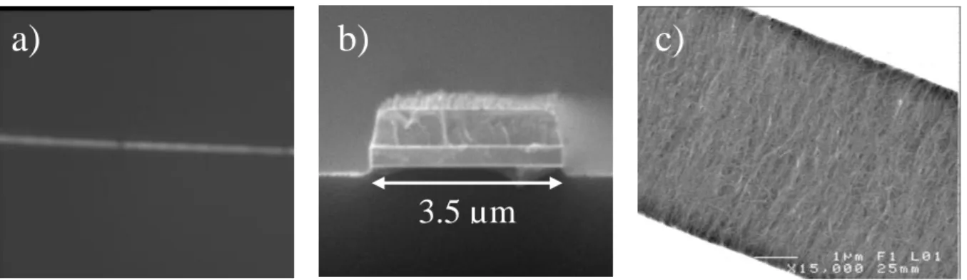
Planar waveguides with air as upper cladding were first characterized. To minimize coupling losses, microlensed fibers with optical mode diameter of 2.2 µm were used to launch a broadband laser source around 1550 nm into the waveguides. Optical propagation at 1550nm in 3.5 mm long-waveguides was confirmed by imaging the output facet of the waveguide on an infrared camera through a high magnification and numerical aperture microscope objective (Fig. 2a).
Fig. 2: a) Intensity profile of the planar SWCNT incorporated-waveguide output, b) SEM picture of ridge SiNx
waveguide with BCB lower cladding (resin was not removed) c) SWCNT aligned by dielectrophoresis between gold electrodes.
Ridge waveguides have been processed using standard i-line photolithography and SF6 based reactive ion etching (Fig. 2b) process for samples with BCB lower cladding layers and SiNx core without
SWCNT. For samples incorporating SWCNT in the waveguide core, worm-like defects occurs during the post-exposure bake. A modification of the thermal steps of BCB curing and photolithographic process could help overcoming these defects9. Interaction of SWCNT with the optical beam could be further improved by aligning SWCNT. To this end, electrophoresis experiments10 have been performed. Fig. 2c shows the preliminary results obtained on the alignment of SWCNT. Transferring this technology to integrated waveguides incorporating CNT should pave the way to the development of efficient devices dedicated to optical signal processing or light emission.
Conclusion:
Waveguides with BCB lower cladding and SWCNT-incorporated SiNx core have been processed. If
problems occurring during photolithographic steps have hindered the optical characterization of ridge waveguides, optical propagation through the planar structure has been observed. These results prove that waveguides with SWCNT incorporated-core could be very promising structures to implement nanoscale light emitters or optical signal processing functions.
References
1 P. Avouris et al., Nature Photonics, 2, 341 (2008)
2 H. Nong et al., Applied Physics Letters, 96, 061109 (2010)
3 S. Wang et al., Nano Letters, 11, 23 (2011) and M. Kinoshita et al., Optics Express, 18, 25738 (2010). 4 E. Gaufrès et al., ACS Nano, 6, 3813 (2012).
5 E. Gaufrès et al., Applied Physics Letters, 96, 231105 (2010). 6 K.K. Chow et al., Applied Physics Letters, 96, 061104 (2010). 7 K.K. Chow et al., Optics Express, 17, 15608 (2009).
8 K.K. Chow et al., Optics Letters, 35, 2070 (2010). 9 D. Bosc et al., Applied Surface Science, 253, 6162 (2007). 10 S. Shekhar et al., ACS Nano, 5, 1739 (2011).