Direct visualization of magnetic vortex pinning in superconductors
Mariela Menghini,1R. B. G. Kramer,1A. V. Silhanek,1 J. Sautner,2V. Metlushko,2K. De Keyser,1 J. Fritzsche,1 N. Verellen,1and V. V. Moshchalkov1
1Nanoscale Superconductivity and Magnetism and Pulsed Fields Group, Institute for Nanoscale Physics and Chemistry (INPAC), K. U. Leuven Celestijnenlaan 200 D, B-3001 Leuven, Belgium
2Department of Electrical and Computer Engineering, University of Illinois, Chicago, Illinois 60607, USA 共Received 7 July 2008; revised manuscript received 15 December 2008; published 1 April 2009兲 We study the vortex structure in a Pb film deposited on top of a periodic array of ferromagnetic square microrings by combining two high-resolution imaging techniques: Bitter decoration and scanning Hall-probe microscopy共SHPM兲. The periodicity and strength of the magnetic pinning potential generated by the square microrings are controlled by the magnetic history of the template. When the square rings are in the magnetized dipolar state, known as the onion state, the strong stray field generated at the domain walls prevents the decoration of vortices. SHPM images show that the stray field generated by the dipoles is much stronger than the vortex field, in agreement with the results of simulations. Real-space vortex imaging has revealed that in the onion state, the corners of the square rings act as effective pinning centers for vortices.
DOI:10.1103/PhysRevB.79.144501 PACS number共s兲: 74.25.Qt, 74.78.Db, 74.78.Na
I. INTRODUCTION
The most attractive hallmark of superconductivity from the technological stand point is the ability to carry electrical current without losses. Unfortunately, this fragile dissipation-less state can be destroyed as a consequence of the motion of quantum flux lines共vortices兲 under the action of the Lorentz force induced by an applied electric current. During the last decades considerable effort has been devoted to prevent this vortex motion by anchoring the vortices using several meth-ods. The vast majority of the research so far has been fo-cused on studying core and electromagnetic pinning mechanisms.1–4 The former is related to the condensation
energy saved when a vortex locates at the position of the pinning center, whereas the latter originates when the super-currents flowing around the vortices in a distance of the or-der of the penetration length, , are deformed due to the presence of the pinning sites. In general, an enhanced vortex core pinning is achieved when the size of the pinning site is similar to the superconducting coherence length .5 In
con-trast to that, there is no optimum size for the electromagnetic pinning as discussed in Refs. 6–9. Lithographically intro-duced micrometer size holes are proved to be efficient pinning centers for vortices in conventional superconductors,10,11 whereas nanometer columnar defects
are more suitable for high-Tc superconductors.5 Further im-provement of the pinning properties can be achieved if be-sides the type and size of individual pinning centers, the geometrical distribution of pinning sites is also considered.8,12–16
An alternative way of creating attractive potential wells for vortices can be realized by exploiting the magnetic inter-action between vortices and nanomagnets. The pioneer work of Alden and Livingston17 showed that embedded magnetic
particles can indeed give rise to a clear enhancement of the critical currents. This early report has been later on corrobo-rated by experiments carried out on other compounds with a better control of the mixing of nanoparticles into the super-conducting matrix.18–29More recently, it has been shown that
the vortex structure can be modified due to the interaction between vortices and a nonuniform magnetic field generated at the surface of the superconductor.30,31An effective
modu-lation of the magnetic field at the surface has been achieved with magnetic particles deposited in a Bitter decoration experiment32 and by the movement of a Bloch wall in a
ferrite garnet film in contact with the superconductor.33 On
the other hand, the fast development of the lithographic tech-niques made it possible to tailor, practically at will, any de-sired magnetic landscape at the sample surface.34–43 In
par-ticular, it has been shown that single36,37,41,43–46 and
multiply47,48 connected structures of magnetic material can act as efficient on/off switchable pinning potential for vorti-ces. The properties of this kind of pinning potential have been explored mainly through macroscopic measurements such as electrotransport and magnetization. Unfortunately, these integrated response techniques conceal the ultimate de-tails of the microscopic world of vortex pinning.
In this work we present results on direct visualization of vortex patterns in a superconducting Pb film deposited on top of a periodic array of square-ring-shaped micromagnets. Real-space vortex arrangements are obtained in this type of hybrid system by combining two noninvasive high-resolution imaging techniques: Bitter decoration and scan-ning Hall-probe microscopy 共SHPM兲. The Bitter decoration experiments have revealed that the strong stray field gener-ated by the square rings in the magnetized state acts as a funnel for the decoration particles, thus impeding the visual-ization of vortices which produce a much weaker local mag-netic field. In addition, the inevitable polarization of the evaporated magnetic clusters due to the external field gives rise to a field-polarity-selected decoration process. One way to overcome these limitations is to image the vortices with SHPM. Images taken with this technique at 4.2 K unveil the actual location of vortices in our superconductor/ferromagnet hybrid system both in the as-grown and the dipolar states.
Previously, vortex imaging in a superconductor/ ferromagnet hybrid shows a preferential location of vortices at magnetic poles of opposite polarity 共compensation effect兲.38In contrast, in our samples vortices sit at the
mag-netic poles with the same polarity. This switching of the pinning potential can be due to the different number of vortex-antivortex 共V-AV兲 pairs generated by the magnetic template, as anticipated in Ref. 49.
II. EXPERIMENTAL DETAILS
The samples studied in this work consist of a square array 共4 m period兲 of Co square rings fabricated by electron-beam共e-beam兲 lithography and subsequent lift-off technique. The density of vortices equals the density of square rings at a matching field of 1.3 Oe. The square rings are 250 nm wide, 25 nm thick, and have a lateral size of 2 m. In order to avoid proximity effects, an insulating buffer layer of 10-nm-thick Ge is deposited on the magnetic array. On top of that, a 50 nm layer of Pb is evaporated.
The electrical transport properties of the sample were studied using a Quantum Design cryostat with conventional electronics. For these measurements the Pb film was evapo-rated onto a predefined photoresist mask patterned into a transport bridge aligned with one of the principal axes of the square lattice of the square microrings. An ac current of 10 A with a frequency of 33 Hz was fed to the sample with a Keithley-6221 current source and the voltage was re-corded using a SR-7265 lock-in amplifier. The temperature stability was within 1 mK.
The Bitter decoration experiments were performed at 4.2 K after cooling down the sample from above the critical temperature, Tc, in the presence of an applied magnetic field perpendicular to the sample surface 关field cooling 共FC兲 ex-periments兴. In this way a homogeneous vortex distribution all over the sample is expected. The scanning Hall-probe microscopy images were obtained using a modified low-temperature scanning Hall-probe microscope 共LTSHPM兲 from Nanomagnetics Instruments. A temperature sensor and a heater were attached to the sample holder allowing fast stabilization and precise measurement of the sample tem-perature. As in the case of the Bitter decorations, the SHPM images were recorded at 4.2 K after FC the sample. The maximum scan area at this temperature is ⬃13⫻13 m2. The Hall voltage was measured in ac mode with a lock-in amplifier at a frequency of 5600 Hz and the rms value of the Hall current was 40 A. The images were recorded in lift-off mode with the Hall sensor at a distance of⬃1 m from the surface of the sample.50
III. TRANSPORT PROPERTIES
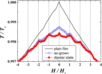
In order to characterize the influence of the array of Co square rings on the superconducting properties of the Pb film, we explored the field and temperature dependence of the resistance, R共H,T兲. The normal-metal/supercondutor 共N/ SC兲 phase boundaries of the Pb with the Co square micror-ings in the as-grown and dipolar state are shown in Fig. 1 together with the results obtained in a coevaporated plain Pb film. The N/SC phase boundary lines were determined by 50% of the normal-state resistance.
The dipolar state, also known as the onion state,51 is the
remanent state after applying a 3000 Oe in-plane field along
one diagonal of the square rings. In this state, head-to-head and tail-to-tail domain walls are formed in two opposite cor-ners of the square rings. Figures2共a兲and2共b兲show, respec-tively, two-dimensional 共2D兲 and three-dimensional 共3D兲 plots of the out-of-plane component of the field, Bz, gener-ated by an individual square ring in the dipolar state obtained by micromagnetic simulation.52 In the simulation we
con-sider a Co square ring with the same dimensions as the one used in the experiment and a saturation magnetization Ms = 140 emu/cm3. In the 2D plot关Fig.2共a兲兴 the red/blue 共light gray/dark gray兲 contrast corresponds to positive and negative intensities of the field, respectively, and the arrows indicate the direction of the in-plane magnetization. The stray field is maximum共either with positive or negative sign兲 at the exter-nal part of the corners where the magnetic moments are head to head and tail to tail 关see Fig.2共b兲兴. In the other two cor-ners there is a small modulation of the field produced by a gentle gradient of the magnetization.
The N/SC phase boundary, Hc2共T兲, of the plain film is linear 共see the solid line in Fig. 1兲 as predicted from the Ginzburg-Landau equations Hc2=关⌽0/22共0兲兴共1−T/Tc兲.1 FIG. 1. 共Color online兲 Normal/superconductor phase boundary for a plain Pb film共line兲 and a Pb film on top of a square array of Co square microrings in the as-grown state共open circles兲 and in the dipolar state共solid squares兲. The temperature is normalized by Tc = 7.2 K and the field by the matching field H1= 1.3 Oe.
Bz (k Oe ) x (µµµµm) y (µµµµm) (a) (b)
FIG. 2. 共Color online兲 共a兲 2D and 共b兲 3D plots of the out-of-plane field, Bz, generated by one magnetic square ring in the dipolar
state obtained by micromagnetic simulation共Ref.52兲. The
dimen-sions of the square ring are the same as in the experiments and the values of the field are calculated at the surface of the square ring. The arrows in 共a兲 indicate the direction of the in-plane magnetic moment.
From the slope of this boundary we estimate the coherence length for our samples共0兲=45.5 nm. Since the BCS coher-ence length for Pb is0⬇83 nm, we can use the dirty limit expression 共0兲=0.855
冑
0l to find the electronic mean-free path l. Using l = 34.1 nm and considering a renormalization53of the penetration length due to the suppression of supercon-ductivity induced by the magnetic array, we obtain 共0兲 ⬇40.5 nm. This calculation indicates that our Pb films are type-II superconductors. This is further confirmed by the de-tection of single-quanta vortices as observed by Bitter deco-rations of our samples.
As a consequence of the stray fields generated by the square microrings in the as-grown state the critical tempera-ture, Tc共H=0兲, of the sample grown on top of the array of magnetic square microrings is lower as compared to the one of the plain film. When the square rings are magnetized in the dipolar state the larger stray fields of the dipoles can locally destroy the superconducting condensate, inducing a further decrease in Tc. In this state, commensurability effects are observed at⫾H1and⫾2H1. It is interesting to note that at⫾3H1the N/SC phase boundary lines of the plain film and the dipolar state merge together. This feature was also ob-served in Al samples deposited on top of Py square rings.47 From this result we can estimate the number of V-AV pairs generated by the stray field of the square rings in the dipolar state. Let us assume that np V-AV pairs per unit cell are created by the square microring array. When H = npH1 all induced antivortices will be compensated by the vortices generated by the applied field. In this case the resultant vor-tex state consists of npvortices induced by the square rings, which is equivalent to applying a field H = npH1 in the plain film 共where no V-AV pairs can be created兲. From that field on, i.e., H =⫾3H1in our particular case, the phase boundary of the plain film and the magnetized sample should overlap as indeed observed. This finding suggests that the estimated number of V-AV pairs generated by the square rings is three.54
IV. BITTER DECORATION RESULTS
The transport measurements presented above show that the array of Co square microrings acts as an effective mag-netic pinning potential for vortices in the superconductor as long as TⱗTc. In order to gain information about the vortex-magnetic dipole interaction we performed Bitter decoration experiments at 4.2 K. One of the main advantages of this technique is the possibility to visualize the distribution of vortices, with single vortex resolution, all over the surface of the sample共of the order of mm2兲.
As-grown state—a FC Bitter decoration experiment car-ried out at 4.2 K in the as-grown state at H = 0 reveals the presence of a disordered state with about 45% of the square rings in a flux-closure state 关see Fig. 3共a兲兴. This particular magnetic state is characterized by a small out-of-plane com-ponent of the stray field, and therefore, no agglomeration of decoration particles is observed on top of these square rings 关Figs.3共b兲and3共e兲兴.55 In the case of decorated square rings
a variety of situations appears; the decoration particles accu-mulate in opposite corners of the square rings, indicating that
those loops are in a dipolar state 关Figs.3共c兲and3共f兲兴 共Ref. 56兲 or neighboring corners appear decorated in square rings that are in the so-called horseshoe state47 关Figs. 3共d兲 and
3共g兲兴. The horseshoe state is such that the net dipolar mo-ment is parallel to the side of the square ring that connects the two decorated corners. In addition, in some cases a single spot along one side or at one corner of the square rings is decorated. This could correspond to the presence of magnetic vortices that generate an out-of-plane field in their center.57
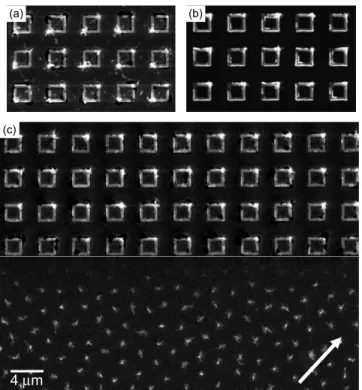
Magnetized state—Fig.4共a兲shows a FC decoration image at H = 0 after the square rings have been magnetized by ap-plying a uniform in-plane field of 3000 Oe parallel to one diagonal of the square rings 关see the white arrow in Fig. 4共c兲兴. As expected, the magnetic dipoles generated by the stray fields have an average magnetic moment along this diagonal, resulting in two intercalated square lattices of posi-tive and negaposi-tive out-of-plane fields. Since the decoration is made on the surface of the superconductor, one would expect that the decorated poles correspond to vortices and antivor-tices located at the corners of the square rings. The same FIG. 3. 共Color online兲 共a兲 Scanning electron microscope 共SEM兲 image of a Bitter decoration performed in the as-grown state at H = 0 and T = 4.2 K. Zoom in of panel 共a兲 at the particular square rings where a共b兲 flux-closure, 共c兲 dipolar, and 共d兲 horseshoe states are observed.关共e兲–共g兲兴 Schematics of a square ring in three different states shown in共b兲–共d兲, respectively. The yellow 共light gray兲 arrows indicate the average direction of the in-plane magnetization. The red 共gray兲 and blue 共black兲 dots in 共f兲 and 共g兲 denote the positive and negative magnetic poles, respectively.
result, namely, the decoration of the corners of the ring where the stray field is maximum, is obtained when decorat-ing directly on top of the Co square rdecorat-ings without the Pb on top共not shown兲.
A possible way to evidence the influence of the SC layer consists in applying a finite field in such a way that both the magnetic poles due to the square rings and the vortices are decorated independently. Figure 4共b兲 shows the result of a magnetic decoration performed at H = H1. Strikingly, the im-age shows that only one corner 共upper right兲 of the square rings is decorated. This result can be in principle attributed to the fact that vortices generated by the applied field sit at the positions where the out-of-plane field of the dipole is negative.38Then, the decoration particles accumulate on the
corners of the square rings where the field of the dipoles is not compensated. Under this circumstance it is expected that for high enough fields 共i.e., strictly speaking H⬎npH1兲, in-terstitial vortices would appear and agglomeration of deco-ration particles should locate in between the square rings. However, decorations performed at higher applied fields, H = 3H1and H = 10H1, still show that only the upper-right cor-ners of the square rings are decorated and no interstitial vor-tices are observed. A similar result is obtained in the case of a decoration performed at H = 0.5H1. As an example, Fig. 4共c兲 shows an image taken in the neighborhood of the boundary between the patterned and nonpatterned regions in a decoration experiment made at H = 3H1. As expected, in the nonpatterned region vortices form a distorted triangular array with a density corresponding to the applied field.
Notice that there are two important points in these results. First, the lack of interstitial vortices in the case H⬎npH1and second the decoration of a single magnetic pole for decora-tions made at H⫽0. In order to understand the origin of the observed lack of interstitial vortices it is necessary to com-pare the field generated by the magnetic dipoles with that associated with vortices. On the surface of the sample, the field generated at the center of the vortex is approximately1
2Hc1= ⌽0
22ln共/兲, 共1兲
where⌽0 is the flux quantum. Using the values of and estimated for our sample we find that the maximum field generated by a vortex at the surface of the sample at 4.2 K is about 200 Oe. On the other hand, from the micromagnetic simulations we can estimate the stray field induced by the square rings at the surface of the superconductor共this corre-sponds to a distance of 50 nm above the square ring surface兲. This calculation shows that the maximum out-of-plane field 共at the corner of the square ring兲 is ⬃1000 Oe, i.e., five times larger than the field of a vortex. Consequently, in a decoration experiment the evaporated magnetic particles “feel” the dipolar field that acts as a funnel accumulating most of the particles at the positions of the poles preventing the decoration of interstitial vortices. This is confirmed by the decoration at the border of the pattern shown in Fig.4共c兲. At first sight it seems that there is a region free of vortices right next to the first row of Co square rings. However, a close inspection of the image shows a row of decoration clumps in that area much less brighter than the rest. Vortices that are at a distance of the order of 4 m from the edge of the pattern are decorated in a normal way. This indicates that one magnetic pole can attract magnetic particles that are at a maximum distance of ⬃6 m共i.e., larger than the separa-tion between magnetic poles兲.
The issue that still remains unsettled is why only one pole of the square rings is decorated when a finite magnetic field is applied. This observation can be ascribed to the fact that the magnetic moment of the evaporated particles aligns with the direction of the applied field at a distance quite far away from the sample surface as schematically represented in Fig. 5. When clusters of polarized particles interact with the di-polar field generated by the square microrings, they are at-tracted to the pole with parallel field orientation and repelled by the other one. Consequently, the absence of decoration particles on the lower-left corner of the square rings is not necessarily due to the presence of vortices but due to the broken symmetry imposed by the applied magnetic field. This is confirmed by the result of a decoration experiment in a sample of Co square rings without a superconducting layer on top. In this case we perform the decoration with the square rings in the dipolar state and a perpendicular applied field of 10 Oe. One would expect that in this situation both poles will appear equally decorated since the applied field is not strong enough to modify the field distribution generated by the square rings. However, it is observed共not shown兲 that the decoration particles only accumulate in the corners of the square rings where the stray field is parallel to the applied
(a) (b)
(c)
4 µm
FIG. 4. Bitter decoration with Co square rings magnetized in the dipolar state at T = 4.2 K and 共a兲 H=0, 共b兲 H=H1, and 共c兲 H = 3H1. In the last case the image is taken at the boundary between the patterned and nonpatterned regions. The white arrow indicates the direction of the in-plane field used to magnetize the square rings.
field. This finding suggests that it is not possible to decorate
either vortices or the stray field generated by magnetic struc-tures when the local magnetic field direction is opposite to the one of the applied field.
V. SCANNING HALL-PROBE MICROSCOPY RESULTS
As-grown state—a possible way to overcome this inher-ent limitation of the Bitter decorations can be achieved by using a less invasive high-resolution technique: SHPM. Fig-ure 6共a兲 shows an image obtained by SHPM after FC a sample with a square array of Co square rings in the as-grown state in a field H⬇1.5H1. In the lower-left part of the image there is a bright and a dark spot next to each other共see circles in the image兲. In addition, over the right edge of the picture there is also a dark spot. These features appear in an image taken at zero applied field 关Fig. 6共b兲兴 as well as in images taken at different applied fields, indicating that they correspond to the out-of-plane stray field generated by the square microrings. After identifying the location of the square rings58共dotted squares in the image兲, it is possible to
see that the pair of bright and dark spots is due to the stray field of a square ring in a horseshoe state关similar to the case shown in Fig. 3共d兲兴. Due to the large intensity difference between the field emanating from the magnetic poles and that produced by the vortices, it is difficult to identify flux lines directly in the image. Therefore, in order to determine the location of vortices it is necessary to remove the contri-bution of the field from the square rings. This is achieved by subtracting from the raw images the field intensity picture taken at H = 0 关see Fig. 6共b兲兴 where no vortices induced by the applied field are present. The result of this subtraction is shown in Fig. 6共c兲 where the vortices are seen as bright spots. We identify the local maxima of intensity as the vortex
positions and depicted them as black dots in Fig. 6共d兲. In most of the cases, vortices sit at the corners of the square rings, forming a rather disordered structure. In the case of the square ring in the horseshoe state a vortex sits along the side of the square ring in between the two poles. It is interesting to note that the values of the magnetic induction of the raw image spans from −10 to 6 G关see the scale bar of Fig.6共a兲兴, while after the subtraction of the H = 0 image the range of intensity is limited to the range 2.5–8 G 关Fig. 6共c兲兴. This difference in scale of magnetic field intensity is due to the stronger field induced by the square microrings as compared to the weaker field emanating from the vortices.
Magnetized state—a different situation appears after mag-netizing the sample by applying an in-plane field of 3000 Oe parallel to one of the diagonals of the square rings, see arrow in Fig.6共e兲. In this case a periodic array of magnetic dipoles is formed, as clearly seen in the image shown in Fig. 6共e兲 obtained after FC the sample down to 4.2 K in a field H ⬇1.5H1.
Similar to the case of the as-grown sample, a subtraction of the H = 0 image关Fig.6共f兲兴 is necessary in order to identify vortex positions 关see Fig. 6共g兲兴. From the field induction scale bars of Figs.6共e兲and6共g兲we can see that the intensity of the dipolar fields is approximately five times larger than the vortex field intensity, in good agreement with the estima-tion made in Sec.IV.
In Figs. 6共h兲–6共j兲 the vortex distributions at H⬇1.5H1,
H⬇−1.5H1, and H⬇3H1, respectively, are shown. The loca-tion of the centers of the positive and negative magnetic poles is indicated by white circles and crosses, respectively. The results of our SHPM experiments show that in the case of FC in a positive field⬇1.5H1, most of the vortices locate on top of the positive poles关Fig.6共h兲兴. The fact that not all of the positive poles are occupied could be due to the influ-ence of intrinsic pinning or due to small inhomogeneities in the sample. When the sign of the field is reversed most of the vortices 共with negative polarity兲 sit on top of the negative poles关Fig.6共i兲兴.
Previous SHPM studies on Pb samples deposited on top of an array of Co/Pt dots with out-of-plane magnetization evidence that vortices sit mainly at positions where the stray field of the micromagnet is parallel to the vortex field.40This
behavior could be understood considering that the dots gen-erate a pinning potential for vortices,
Um共r兲 = −
冕
Vfm共r
⬘
兲 · B共r − r⬘
兲dr⬘
, 共2兲 where m is the magnetization of the dot, B is the field of the vortex, and the integration is done over the volume of the ferromagnet. This potential has a minimum on top of the dots when the applied field H 共and consequently the field of the vortices兲 is parallel to the magnetization direction. On the other hand, similar experiments in Pb samples with arrays of bars with in-plane magnetization show38 alsofield-polarity-dependent pinning but now due to the interaction between vortices and vortex-antivortex pairs generated by the mag-netic bars. In this case vortices sit at the poles where the stray field is opposite to the applied field. Theoretical calcu-FIG. 5. 共Color online兲 Schematic presentation of the
accumula-tion of polarized decoraaccumula-tion particles on top of one corner of the Co square microrings 共see text兲. The black arrows indicate the stray field induced by the magnetized square ring while the gray arrow denotes the direction of the applied field. On the upper part of the image the filament that generates the decoration particles 共red spheres兲 is shown.
lations of the interaction between vortices and a ferromagnet with in-plane magnetization demonstrate49 that whether the
vortex will be pinned by one or the other pole of the micro-magnet depends on the strength of the micromicro-magnet magne-tization. In the case where the magnetization is large enough to induce a vortex-antivortex pair in the superconductor, the equilibrium position of a vortex generated by an applied field is the result of the balance among vortex-micromagnet, vortex-vortex, and vortex-antivortex interactions. It is impor-tant to mention that in the calculations only the interaction of a single vortex with one magnetic microstructure that can generate, at maximum, one vortex-antivortex pair is consid-ered. Unfortunately, so far there is no prediction of the lowest-energy vortex state considering also the interaction with other vortices generated by the applied field and with more than one induced vortex-antivortex pair. In our experi-ments we observe that at low densities vortices sit mostly on
top of the corners of the square rings 关Figs.6共h兲 and6共i兲兴. Therefore we can assure that the magnetic square microrings act as effective pinning centers for vortices even when low-ering the temperature down to 4.2 K.
Finally, when the field is further increased, SHPM FC experiments show that vortices start to locate also at the negative poles of the micromagnets, see, for example, the vortex distribution at H⬇3H1 shown in Fig. 6共j兲. Few vor-tices sit at the corners of the square rings where the out-of-plane field is very small共for example, see the square micror-ing at the upper-left corner of the image兲 but no vortices are seen to locate in the interstitial sites in between the square rings. A possible explanation for the observed vortex con-figuration is that vortices placed at the positive poles gener-ate a caging potential59 with a minimum in the location of
the negative magnetic poles. As a counterpart, the force ex-erted on the vortices by the negative magnetic poles 关see FIG. 6. 共Color online兲 关共a兲 and 共b兲兴 Raw SHPM images taken after FC down to T=4.2 K in a field H⬇1.5H1and H = 0, respectively, with the square rings in the as-grown state. The circles indicate regions of strong stray fields generated by the square rings that are in a magnetized state.共c兲 Vortex image in the as-grown state at H⬇1.5H1. This image is obtained by subtracting the image共b兲 共H=0兲 from 共a兲. In共d兲 the black dots indicate the vortex locations that were identified as local maxima in 共c兲. 关共e兲 and 共f兲兴 Raw images taken after FC in a field H⬇1.5H1and H = 0, respectively, with the square rings in the dipolar state.共g兲 Vortex image at H⬇1.5H1obtained by subtracting共f兲 from共e兲. Vortex location in the dipolar state at 共h兲 H⬇1.5H1,共i兲 H⬇−1.5H1, and共j兲 H⬇3H1. In all images the dotted lines indicate the positions of the square rings, the field of view is 12.6⫻12.6 m2and the color共gray兲 scale bars correspond to the magnetic induction in units of Gauss. In共e兲 the black arrow indicates the orientation of the in-plane field used to magnetize the square microrings.
Eq. 共2兲兴 would tend to repel vortices from those positions. Thus, the observed vortex distribution at higher densities seems to be a result of the balance between vortex-vortex and vortex-magnetic pole interactions. Our SHPM experi-ments in the magnetized state show that the corners of the square rings, both with magnetization parallel and opposite to the vortex field, represent effective pinning sites for vor-tices.
VI. CONCLUSIONS
We have studied the influence of an array of Co square microrings on the superconducting properties of a Pb film. From transport measurements we observe that the stray fields induced by the magnetic loops cause a reduction in Tcwith respect to a plain Pb film, in agreement with earlier reports. Furthermore, when the square rings are in a dipolar state, matching features are observed. This indicates that the mi-cromagnets act as pinning centers for vortices near the N/SC phase boundary line. On the other hand, Bitter decorations at 4.2 K in the as-grown state show that almost half of the square rings are in a flux-closure state. In the dipolar state, the strong stray magnetic field associated with the square rings act as funnels for the magnetic decoration particles. Due to this effect, the particles accumulate on the corners of the square rings, preventing the decoration of vortices. Our results also suggest that it is not possible to decorate regions where the local magnetic field direction is opposite to the one of the applied field. SHPM experiments in the as-grown
state show that at low temperatures, the square rings act as pinning centers even if they are in a flux-closure state. Be-sides, the images obtained in FC experiments confirm that the field induced by the square rings in the dipolar state is much larger than the field of the vortices. This result is con-sistent with the results obtained by micromagnetic simula-tions. Moreover, FC images taken in the dipolar state and at low vortex densities show that the poles with magnetization parallel to the applied field create strong pinning sites for vortices. At higher fields, the opposite poles can also act as preferential sites for vortices, suggesting that the resultant vortex structure is a consequence of the competition between vortex-vortex and vortex-magnetic dipole interactions. Our results indicate the necessity of a theoretical model of a superconductor/ferromagnet hybrid system which takes into account vortex-vortex interactions and the interaction of a vortex with more than one induced vortex-antivortex pair.
ACKNOWLEDGMENTS
We would like to thank F. de la Cruz, Y. Fasano, R. Luccas, P. Mispelter, and P. De Greef for useful technical discussions and W. Gillijns for a careful reading of the paper. This work was supported by the Research Fund K.U. Leuven under Grant No. GOA/2004/02, the Fund for Scientific Research-Flanders FWO-Vlaanderen, the Belgian Inter-University Attraction Poles IAP, the European ESF NES pro-grams, the U.S. NSF under Grant No. ECCS-0823813, and CNM ANL under Grants No. Nr.468 and Nr.470. A.V.S. is grateful for the support from the FWO-Vlaanderen.
1M. Tinkham, Introduction to Superconductivity, 2nd ed. 共McGraw-Hill, New York, 1996兲.
2A. E. Campbell and J. E. Evetts, Adv. Phys. 21, 199共1972兲. 3G. Blatter, M. V. Feigeľman, V. B. Geshkenbein, A. I. Larkin,
and V. M. Vinokur, Rev. Mod. Phys. 66, 1125共1994兲. 4A. Buzdin and D. Feinberg, Physica C 235-240, 2755共1994兲. 5L. Civale, A. D. Marwick, T. K. Worthington, M. A. Kirk, J. R.
Thompson, L. Krusin-Elbaum, Y. Sun, J. R. Clem, and F. Holtzberg, Phys. Rev. Lett. 67, 648共1991兲.
6G. S. Mkrtchyan and V. V. Shmidt, Sov. Phys. JETP 34, 195 共1972兲.
7N. Takezawa and K. Fukushima, Physica C 228, 149共1994兲. 8V. V. Moshchalkov, M. Baert, V. V. Metlushko, E. Rosseel, M. J.
Van Bael, K. Temst, Y. Bruynseraede, and R. Jonckheere, Phys. Rev. B 57, 3615共1998兲.
9H. Nordborg and V. M. Vinokur, Phys. Rev. B 62, 12408共2000兲. 10A. Bezryadin and B. Pannetier, J. Low Temp. Phys. 98, 251
共1995兲.
11V. V. Moshchalkov, M. Baert, V. V. Metlushko, E. Rosseel, M. J. Van Bael, K. Temst, Y. Bruynseraede, and R. Jonckheere, J. Phys. IV 6, C3-335共1996兲.
12C. Reichhardt and C. J. Olson Reichhardt, Phys. Rev. B 76, 094512共2007兲.
13M. Kemmler, C. Gurlich, A. Sterck, H. Pohler, M. Neuhaus, M. Siegel, R. Kleiner, and D. Koelle, Phys. Rev. Lett. 97, 147003
共2006兲.
14J. E. Villegas, M. I. Montero, C.-P. Li, and Ivan K. Schuller, Phys. Rev. Lett. 97, 027002共2006兲.
15V. Misko, S. Savel’ev, and F. Nori, Phys. Rev. Lett. 95, 177007 共2005兲.
16A. V. Silhanek, W. Gillijns, V. V. Moshchalkov, B. Y. Zhu, J. Moonens, and L. H. A. Leunissen, Appl. Phys. Lett. 89, 152507 共2006兲.
17T. H. Alden and J. D. Livingston, Appl. Phys. Lett. 8, 6共1966兲. 18A. Snezhko, T. Prozorov, and R. Prozorov, Phys. Rev. B 71,
024527共2005兲.
19N. D. Rizzo, J. Q. Wang, D. E. Prober, L. R. Motowidlo, and B. A. Zeitlin, Appl. Phys. Lett. 69, 2285共1996兲.
20J.-Q. Wang, N. D. Rizzo, D. E. Prober, L. R. Motowidlo, and B. A. Zeitlin, IEEE Trans. Appl. Supercond. 7, 1130共1997兲. 21N. M. Suleimanov, P. N. Togulev, V. V. Bazarov, and I. B.
Khaibullin, Physica C 404, 363共2004兲.
22D. Stamopoulos, M. Pissas, and E. Manios, Phys. Rev. B 71, 014522共2005兲.
23D. Stamopoulos, E. Manios, M. Pissas, and D. Niarchos, Physica C 437-438, 289共2006兲.
24T. Kuroda, T. Nakane, H. Uematsu, and K. Kumakura, Super-cond. Sci. Technol. 19, 1152共2006兲.
25P. N. Togoulev, N. M. Suleimanov, and K. Conder, Physica C
26A. Palau, J. L. MacManus-Driscoll, and M. G. Blamire, Super-cond. Sci. Technol. 20, S136共2007兲.
27S. Haindl, M. Weisheit, V. Neu, L. Schultz, and B. Holzapfel, Physica C 463-465, 1001共2007兲.
28A. Palau, H. Parvaneh, N. A. Stelmashenko, H. Wang, J. L. Macmanus-Driscoll, and M. G. Blamire, Phys. Rev. Lett. 98, 117003共2007兲.
29S. Haindl, M. Weisheit, T. Thersle, L. Schultz, and B. Holzapfel, Supercond. Sci. Technol. 21, 045017共2008兲.
30S. Erdin, I. F. Lyuksyutov, V. L. Pokrovsky, and V. M. Vinokur, Phys. Rev. Lett. 88, 017001共2001兲.
31G. Carneiro, Phys. Rev. B 72, 144514共2005兲; Physica C 432, 206共2005兲.
32Y. Fasano, J. A. Herbsommer, F. de la Cruz, F. Pardo, P. L. Gammel, E. Bucher, and D. J. Bishop, Phys. Rev. B 60, R15047 共1999兲.
33P. E. Goa, H. Hauglin, A. A. F. Olsen, D. Shantsev, and T. H. Johansen, Appl. Phys. Lett. 82, 79共2003兲.
34O. Geoffroy, D. Givord, Y. Otani, B. Pannetier and F. Ossart, J. Magn. Magn. Mater. 121, 223共1993兲; Y. Otani,B. Pannetier, J. P. Nozieres, and D. Givord, ibid. 126, 622共1993兲.
35J. I. Martín, M. Velez, J. Nogues, and I. K. Schuller, Phys. Rev. Lett. 79, 1929共1997兲.
36M. J. Van Bael, K. Temst, V. V. Moshchalkov, and Y. Bruynser-aede, Phys. Rev. B 59, 14674共1999兲.
37L. van Look, M. J. van Bael, K. Temst, J. G. Rodrigo, M. Mo-relle, V. V. Moshchalkov, and Y. Bruynseraede, Physica C 332, 356共2000兲.
38M. J. Van Bael, J. Bekaert, K. Temst, L. Van Look, V. V. Mosh-chalkov, Y. Bruynseraede, G. D. Howells, A. N. Grigorenko, S. J. Bending, and G. Borghs, Phys. Rev. Lett. 86, 155共2001兲. 39M. Lange, M. J. Van Bael, Y. Bruynseraede, and V. V.
Mosh-chalkov, Phys. Rev. Lett. 90, 197006共2003兲.
40M. J. Van Bael, M. Lange, S. Raedts, V. V. Moshchalkov, A. N. Grigorenko, and S. J. Bending, Phys. Rev. B 68, 014509共2003兲. 41J. E. Villegas, S. Savel’ev, F. Nori, E. M. Gonzalez, J. V. An-guita, R. Garcia, and J. L. Vicent, Science 302, 1188共2003兲. 42Y. Fasano, M. De Seta, M. Menghini, H. Pastoriza, and F. de la
Cruz, Solid State Commun. 128, 51共2003兲.
43W. Gillijns, A. V. Silhanek, and V. V. Moshchalkov, Phys. Rev. B
74, 220509共R兲 共2006兲.
44J. E. Villegas, K. D. Smith, L. Huang, Y. Zhu, R. Morales, and I. K. Schuller, Phys. Rev. B 77, 134510共2008兲.
45A. Hoffmann, L. Fumagalli, N. Jahedi, J. C. Sautner, J. E. Pear-son, G. Mihajlovic, and V. Metlushko, Phys. Rev. B 77, 060506共R兲 共2008兲.
46J. S. Neal, M. V. Milošević, S. J. Bending, A. Potenza, L. San Emeterio, and C. H. Marrows, Phys. Rev. Lett. 99, 127001 共2007兲.
47A. V. Silhanek, N. Verellen, V. Metlushko, W. Gillijns, F.
Gozzini, B. Ilic, and V. V. Moshchalkov, Physica C 468, 563 共2008兲; A. V. Silhanek, W. Gillijns, V. V. Moshchalkov, V. Metlushko, and B. Ilic, Appl. Phys. Lett. 89, 182505共2006兲. 48N. Verellen, A. V. Silhanek, V. Metlushko, W. Gillijns, F.
Gozzini, B. Ilic, and V. V. Moshchalkov, Appl. Phys. Lett. 93, 022507共2008兲.
49M. V. Milošević and F. M. Peeters, Phys. Rev. B 69, 104522 共2004兲.
50In our scanning Hall-probe microscope a scanning tunneling mi-croscope共STM兲 tip and a Hall probe are integrated in the same chip. The STM tip is used to approach the Hall probe to the sample surface, i.e., the tip is in contact with the surface when a tunneling current is detected. This approach is made on top of the highest point of the sample共top-right corner in our images兲. In a lift-off mode operation the STM tip is retracted at a certain distance 共lift-off distance兲 from the sample surface. Since the Hall probe is located 15 m behind the STM tip, the distance between the Hall probe and the sample surface is larger than the lift-off distance. In our case we estimate a tilt angle of ⬃3°. Therefore, since during the experiments the lift off is 200 nm the distance between the Hall sensor and the sample is ⬃1 m at the approaching point. This separation increases as the image is scanned, giving rise to a decrease in contrast in the images from top to bottom. For more details see S. J. Bending, Adv. Phys.
48, 449共1999兲.
51X. B. Zhu, P. Grutter, V. Metlushko, and B. Ilic, J. Appl. Phys.
93, 7059共2003兲.
52Micromagnetic simulations are performed with a public avail-able code from NIST共http://math.nist.gov/oommf兲.
53A. Wahl, V. Hardy, J. Provost, Ch. Simon, and A. Buzdin, Physica C 250, 163共1995兲.
54Note that this is an approximate estimate.
55The bright edges of the square microring shown in Fig.3共b兲are due to the charging effects during the acquisition of the image with SEM.
56In a decoration experiment regions with positive and negative out-of-plane local magnetic fields are not distinguished from each other since the decoration particles are sensitive to the field gradient independently of the field direction.
57A. V. Silhanek, W. Gillijns, V. V. Moshchalkov, V. Metlushko, F. Gozzini, B. Ilic, W. C. Uhlig, and J. Unguris, Appl. Phys. Lett.
90, 182501共2007兲.
58In order to determine the location of the square rings an out-of-plane field of the order of 5000 Oe was applied after doing the FC experiments in the as-grown state. Subsequently a SHPM image was taken where the square rings appear as bright spots due to the finite out-of-plane component of the magnetization. 59I. B. Khalfin and B. Ya. Shapiro, Physica C 207, 359共1993兲; E.
Rosseel, M. Van Bael, M. Baert, R. Jonckheere, V. V. Mosh-chalkov, and Y. Bruynseraede, Phys. Rev. B 53, R2983共1996兲.
![[PDF] Formation avancé sur l'utilisation des Applications Perl | Formation informatique](data:image/gif;base64,R0lGODlhAQABAIAAAP///wAAACH5BAEAAAAALAAAAAABAAEAAAICRAEAOw==)