HAL Id: hal-00873978
https://hal.archives-ouvertes.fr/hal-00873978
Submitted on 9 Mar 2021
HAL is a multi-disciplinary open access
archive for the deposit and dissemination of
sci-entific research documents, whether they are
pub-lished or not. The documents may come from
teaching and research institutions in France or
abroad, or from public or private research centers.
L’archive ouverte pluridisciplinaire HAL, est
destinée au dépôt et à la diffusion de documents
scientifiques de niveau recherche, publiés ou non,
émanant des établissements d’enseignement et de
recherche français ou étrangers, des laboratoires
publics ou privés.
An efficient on-chip configuration infrastructure for a
flexible multi-ASIP turbo decoder architecture
Vianney Lapotre, Hübner Michael, Guy Gogniat, Purushotham Murugappa
Velayuthan, Amer Baghdadi, Jean-Philippe Diguet
To cite this version:
Vianney Lapotre, Hübner Michael, Guy Gogniat, Purushotham Murugappa Velayuthan, Amer
Bagh-dadi, et al.. An efficient on-chip configuration infrastructure for a flexible multi-ASIP turbo decoder
ar-chitecture. ReCoSoC 2013 : 8th IEEE International Workshop on Reconfigurable and
Communication-Centric Systems-on-Chip, Jul 2013, Darmstadt, Germany. �10.1109/ReCoSoC.2013.6581518�.
�hal-00873978�
An efficient on-chip configuration infrastructure for a flexible multi-ASIP turbo decoder
architecture
Vianney Lapotre∗, Michael H¨ubner†, Guy Gogniat∗, Purushotham Murugappa‡, Amer Baghdadi‡and Jean-Philippe Diguet∗
∗
Univ. Bretagne Sud, UMR6285, Lab-STICC, F56100 Lorient, France. Email: [email protected]
†Rurh-Universit¨at Bochum, ESIT, Bochum, Germany. Email: [email protected]
‡
Telecom Bretagne, UMR6285, Lab-STICC, F29200 Brest, France. Email: [email protected]
Abstract—Dynamic reconfiguration of multiprocessor platforms is an important challenge for System-on-Chip designers. Addressing this issue is mandatory in order to manage the increasing number of applications and execution conditions that multiprocessor platforms have to face. In this paper, a novel configuration infrastructure for the UDec multi-ASIP turbo decoder architecture is presented. Our approach leads to split the interconnection architecture in two subsets, one dedicated for data and another dedicated for configuration. Indeed both types of communication do not have the same requirements. Our novel configuration infrastructure, which proposes an area efficient and low latency solution, has been validated through a two-step approach. First a SystemC/VHDL mixed simulation model has been developed to perform an early performance evaluation, second a hardware FPGA prototype has been built. Results show that up to 64 processing elements can be dynamically configured in 5.352 µs.
Keywords-Multi-ASIP; Reconfiguration; Self-adaptation; Turbo de-coder;
I. INTRODUCTION
The increasing demand of flexibility, energy efficiency and throughput requirement for telecommunication applications leads designers to build dynamically reconfigurable application specific multiprocessor platforms. In this context the UDec architecture presented in [1] is a flexible multi-ASIP turbo decoder. It con-sists of Application Specific Instruction set Processors (ASIP) interconnected through a Network on Chip (NoC) dedicated to data exchanges. The flexibility of the UDec architecture comes from a configuration memory associated to each ASIP. Each time a new configuration has to be launched, each ASIP downloads the corresponding parameters from its configuration memory. This flexibility must rely on a configuration infrastructure in order to transfer new parameters to configuration memories. Moreover, due to the increasing requirements in terms of throughput and low latency, the available reconfiguration time between two data frames decreases in recent communication standards. Fig. 1.a illustrates a scenario in which three frames are serially decoded with three different configurations. The configuration latency of a frame
(noted ∆tConf ig) is constrained by the previous frame decoding
duration. Fig. 1.b shows the frame duration for a frame size of 2048 bits depending on the decoding throughput. This example illustrates how the available time to decode a frame critically decreases when the throughput requirement increases. Consequently, reaching a reconfiguration time below 10 µs will be a key concern to face expected throughput of future communication standards like LTE Advanced which provides throughput up to 1Gbps. Management of dynamic reconfiguration of such multiprocessor channel decoder is not well addressed in the literature. To face these requirements this paper proposes an optimized on-chip configuration infrastructure dedicated to configuration data transfer in a dynamically reconfig-urable application specific multiprocessor platform.
Several configuration infrastructures and strategies have been
0 5 10 15 20 25 30 35 40 45 50 10 80 150 220 290 360 430 500 570 640 710 780 850 920 990 fr a m e d u ra ti o n ( in µ s) LTE cat.4 (2011) (150 Mbps ; 14 µs) LTE Advanced (2014) (1 Gbps ; 2.5 µs) HSPA + (2010) (84 Mbps ; 24 µs) LTE cat.5 (2011) (300Mbps ; 7 µs) Config. Frame n+1 Config. Frame n
Frame n-1 Frame n Frame n+1
Config. Frame n+2
Time ΔtConfig(n+1)
a) Configuration latency constraint Decoding
Configuration
Frame duration (n)
10 80 150 220 290 360 430 500 570 640 710 780 850 920 990 Throughput (in Mpbs)
b) Frame decoding duration for a 2048 bits frame
Figure 1. Configuration latency constraint and frame duration
developed for recent reconfigurable multiprocessor architectures dedicated to multimedia and telecommunication applications. In [2] and [3], configurations are distributed among several configuration servers that provide configuration data on demand. In [2] configura-tion servers are dedicated resources embedded in an heterogeneous platform while in [3] each cluster of DSPs corresponds to a config-uration server that provides a complete or a part of a configconfig-uration. In both approaches, a unique NoC is used for application and configuration data as it is assumed that configuration transfers do not negatively impact the application data throughput. However, in [1] the NoC is designed for interleaving process and cannot be used to configure ASIPs without reducing data throughput. Indeed, this NoC consists of two unidirectional butterfly NoCs that are optimized for application data. In this case, an additional configuration interconnect is mandatory to provide configuration mechanisms that do not lower decoding performances.
In [4], clusters of DSPs are connected through a NoC for appli-cation data exchanges and a dedicated bus is used for both control and configuration transfers. A central controller sends configuration commands to local cluster controllers that download configurations from a central shared memory using DMA accesses. Thus, each component connected to the bus is a master. Extra hardware is required in order to manage and to arbitrate these transfers. In this paper, we propose a dedicated configuration infrastructure optimized for the architecture described in [1]. It consists of a low complexity unidirectional on-chip bus implementing multicast mechanisms and incremental data burst in order to reduce the configuration latency. Moreover, a configuration manager, which is the only master on the bus, is in charge of the configuration generation at run-time. Compared to existing efforts our approach provides both a very low configuration latency and a low area
overhead. Several optimizations have been developed in order to minimize the cost of the configuration infrastructure. To validate our contribution we have adopted a two-step evaluation process based on a virtual prototyping approach. In a first step a Sys-temC/VHDL mixed simulation model has been used to perform an early evaluation of our solution. Then, in a second step a FPGA prototype has been built to measure the actual hardware cost and performance.
The rest of this paper is organized as follows. Section II introduces the UDec architecture. Section III highlights the main issues that need to be addressed in order to build an efficient configuration infrastructure while section IV describes the proposed bus-based solution. Section V provides first evaluations through a SystemC/VHDL mixed model. Section VI presents the FPGA implementation results. Finally section VII concludes the paper.
II. MULTI-ASIPTURBO DECODER
A. UDec architecture
The turbo decoding system diagram is presented in Fig. 2. It consists of component decoders that exchange extrinsic information
through an interleaver (Π) and a deinterleaver (Π−1) processes. The
component decoder 1 receives Log-Likelihood Ratio (LLR) from a demapper for each bit of a data frame in the natural order while component decoder 0 receives LLR in interleaved order. Then, iterative decoding algorithm is performed to decode the data frame.
Component decoder 0 Component decoder 1 π-1 π π Hard. dec Channel LLR
Figure 2. Turbo decoding system
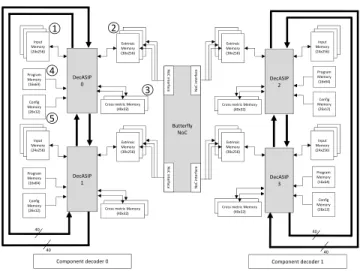
The UDec turbo decoder architecture [1] is shown in Fig. 3. It consists of two rows of DecASIPs interconnected through a butterfly topology NoCs [5]. Each row corresponds to a component decoder. In the example of Fig. 3, four ASIPs are organized in 2 component decoders respectively built with 2 ASIPs. Within each component decoder the ASIPs are connected by two 80-bit buses for boundary state metrics exchange. The DecASIP implements the Max-Log MAP algorithm as described in [6]. It supports both single and double binary convolutional turbo codes and implements radix-4 trellis compression technique for SBTC mode. Large frames are processed by dividing the frame into N windows each with a maximum size of 64 symbols. Each ASIP can manage a maximum of 12 windows. The DecASIP is associated with 3 memory banks of size 24x256 used to store the input
channel LLR values ¬. There are also another 3 banks of size
30x256 used for extrinsic information storing . Each ASIP is
further equipped with two 40x32 memories which hold state values ®. Moreover, each ASIP is configured through a program ¯ and
a configuration memory °. The configuration memory contains
all parameters required to perform the initialization of the ASIP while the program memory contains the instructions in order to perform the decoding algorithm. Since the DecASIP is designed to work in a multi-ASIP architecture as described in [1], it requires several parameters to deal with a subblock of the data frame and
40
40
40
40
Component decoder 0 Component decoder 1 Butterfly NoC N o C in te rfa ce N o C in te rfa ce No C in te rf a ce N o C in te rf a ce DecASIP 0 DecASIP 2 Extrinsic Memory (30x256) Program Memory (16x64) Config Memory (26x12) Input Memory (24x256)
Cross metric Memory (40x32) DecASIP 1 Extrinsic Memory (30x256) Program Memory (16x64) Config Memory (26x12) Input Memory (24x256)
Cross metric Memory (40x32) Extrinsic Memory (30x256) Program Memory (16x64) Config Memory (26x12) Input Memory (24x256)
Cross metric Memory (40x32) DecASIP 3 Extrinsic Memory (30x256) Program Memory (16x64) Config Memory (26x12) Input Memory (24x256)
Cross metric Memory (40x32)
1 2
3 5
4
Figure 3. UDec system architecture example with 2x2 ASIPs
several parameters to configure the ASIP mode. Concerning the subblock partitioning, each ASIP is configured with the size and the number of windows it has to decode. Furthermore, the last window size can be different so it corresponds to an additional parameter. In a single binary turbo code mode, the address of the tail bits in memory, the size and the number of windows for the tail bits have to be configured. Parameters for the ASIP mode correspond to the location of the ASIP in the architecture, the number of ASIPs required, the parameter which defines if the current ASIP is in charge of tail bits or not, the target standard (3GPP-LTE, WIMAX, or DVB-RCS) and the scaling factor for extrinsic information. Finally, some seed values are necessary for address generation in order to exchange information over the NoC that connects the ASIPs of each decoder component. All these parameters are required for a configuration of an ASIP within the platform.
B. UDec configuration
The behavior of the UDec turbo decoder is dependent of the parameters loaded in the configuration memory of each ASIP. In order to improve the reconfiguration step, it is essential to optimize the organization of the configuration memory. The configuration parameters stored in the configuration memory can be divided in four categories: 1) domain dependent, 2) identical for all ASIPs, 3) different for all ASIPs and 4) different for the last two ASIPs which decode the tail bits in single binary turbo code mode. A smart memory organization allows an efficient broadcasting of the configuration parameters to the required ASIPs. Thus, three groups which occupy three different parts of the configuration memory have been defined.
Table I shows the configuration memory organization. A config-uration consists of 286 bits and is organized as follows:
• From address @0 to @1, parameters can be different for each
ASIP. Furthermore, to optimize the initialization step of ASIP, the parameter Tail which indicates if the ASIP has to perform or not the tail bits is included in this group. Only the last two ASIPs have to deal with the tail bits in single binary turbo code mode.
• From address @2 to @6, parameters are identical for ASIPs
bit 25 24 23 22 21 20 19 18 17 16 15 14 13 12 11 10 9 8 7 6 5 4 3 2 1 0
@0 - Tail ASIPId
@1 Turbo Seed 0 Turbo Seed 1
@2 - TurboInitIteration Maxiteration State NumSteps
@3 Turbo Step 0 Turbo Step 1
@4 Turbo Step 2 Turbo Step 3
@5 Turbo Step 4 Turbo Step 5
@6 Turbo Step 6 Turbo Step 7
@7 - @ Tail bits Scaling Factor Mode
@8 Turbo PrevStep Blocklength in bits
@9 - NumASIPs StepIndex WindowSize LastWindowSize
@10 - CurrentWindowN norm CurrentWindowID tail WindowN tail
Table I
ASIP CONFIGURATION MEMORY
• From address @7 to @10, parameters are the same for all
ASIPs.
This organization allows an efficient and fast reconfiguration at the platform level. Indeed, multicast mechanisms can be used to load the configuration in order to minimize the data transfer load. In this context, two multicast transfers are necessary to send domain dependent parameters to corresponding ASIPs and one multicast transfer for parameters that are the same for all ASIPs. Finally, unicast transfers are used to load the ASIP dependent parameters. Once configurations are loaded in ASIPs configuration mem-ories, ASIPs can be launched as soon as input data are ready. The configuration parameters are then read from the configuration memory and stored in each ASIP internal registers. When this initialization phase is finished the decoding phase can start. Note that a new configuration can be downloaded into configuration memories while computation is performed, such an approach minimizes the reconfiguration latency and allows the execution scheme described in Fig. 1.a.
Besides the ASIPs, the UDec platform implements flexible elements as a controller, an input interface, the two buses for boundary state metrics exchange and the Butterfly NoC. The controller is in charge of the computation scheduling depending of the mode (serial or shuffle decoding), the number of decoding iterations, and the number and location of the selected ASIPs. The input interface is configured to spread the symbols coming from a demapper to the inputs memory of selected ASIPs depending of the frame size, the selected standard, the number and the location of the selected ASIPs. Finally, the two buses for boundary state metrics exchange and the Butterfly NoC Network Interfaces (NIs) are configured to take into account the number and location of the selected ASIPs. For that purpose, an extra configuration memory attached to the platform controller is added. When a new configuration is loaded, the controller launches an initialization phase to read configuration parameters in this memory and store them into configuration registers.
III. MAIN CHALLENGES FOR AN EFFICIENT CONFIGURATION INFRASTRUCTURE
Dynamic reconfiguration of flexible multiprocessor platforms is one of the main challenges for system designers. This issue is important, especially when dealing with multiprocessor plat-forms where no global communication interconnect can be shared between application and configuration data. In this case, it is mandatory to implement a communication infrastructure dedicated to configuration data. In the UDec architecture, the 80-bit buses and
the Butterfly NoC are optimized and dedicated to data exchange between DecASIPs. These interconnections can not be used to transfer the configuration data. To build an efficient solution, the
configuration infrastructurehas to take into account the following
requirements: 1) Low complexity, 2) Multicasting mechanism and 3) Burst transfer.
A. Low complexity
The configuration infrastructure only manages configuration memories updates. Thus, this extra hardware must have a minimal impact on the global design complexity in terms of area overhead. When designing a communication architecture in a multiprocessor platform, two main technologies are available: Network on Chip or On-Chip Bus. Last decade has seen the huge adoption of Networks on Chip in complex System on Chip to mainly enhance the throughput and the scalability compared to a bus-based com-munication infrastructure. However, the design of a comcom-munication interconnect dedicated to configuration data does not require such a complex approach. Indeed, broadcasting can be defined as a unidirectional communication between a reconfiguration manager that generates and downloads configuration data to one or a group of processing elements that have to be configured. Hence, there is not transfer concurrency issue, and a unique component, called Master, is able to initiate a transfer. Moreover, we assume that the configuration manager is, at any time, aware of the configuration state of the platform. Thus, no read operations are necessary to check a status or the presence of a particular configuration in a given processing element. These features lead to a bus-based structure that provides a simple communication interconnect for this particular context.
B. Multicasting and selection
The UDec platform is configured through the DecASIP ration memories. As shown in Section II-B, the DecASIP configu-ration memory is organized in order to allow multicast mechanisms for an efficient and fast configuration of the multi-ASIP platform. Moreover, depending on the application requirements, the number of activated DecASIPs to perform a given configuration can be tuned at run-time. Hence, a mechanism of processor selection has to be introduced in order to send configuration data to activated DecASIPs only.
C. Incremental data burst transfer
The last point to build an efficient configuration infrastructure for the UDec platform is related to the transfer mode. Since some
Mem.@ Data T_enable Dest. @ Selector T _ in it D _ e n a b le D a ta B a se . @ D e st . @ Configuration Manager 26 8 8 26 8 8 Configuration memory 0 Master Interface (MI) Slave Interface 0 (SI_0) Slave Interface 1 (SI_1) Slave Interface N (SI_N) 26 8 D a ta M e m . @ W _ e n a b le Configuration memory 1 26 8 D a ta M e m . @ W _ e n a b le Configuration memory N 26 8 D a ta M e m . @ W _ e n a b le Enable SI_0 Enable SI_1 Enable SI_N T_enable
Figure 4. Architecture of the proposed bus interconnect
of the configuration data has to be loaded in adjacent parts in the configuration memory, all related transfers can be defined as a burst starting from a base address in the configuration memory. For example, based on the DecASIP memory organization of Table I, configuration data identical for all DecASIPs can be incrementally transferred starting from the base address @7. Four incremental transfers are then performed.
Many On-Chip Buses have been developed these last years that propose different topologies and different communication proto-cols. Representative On-chip Buses are the AMBA [7], the Core-Connect [8] or the Avalon bus [9]. Unfortunately, these solutions do not support multicast. Work presented in [10] supports multicast but this solution implements complex arbitration mechanisms and communication protocols that are not necessary in our context. The Fast Simplex Link (FSL) [11] proposes a low complexity unidirectional bus for data transfer. Unfortunately multicast is not supported. It is thus mandatory to propose an optimized bus dedicated to configuration data that could be used for the UDec platform in order to reach the configuration latency challenge.
IV. CONFIGURATION INFRASTRUCTURE
To address the main issues highlighted in Section III, we propose a new bus-based communication infrastructure as well as the associated communication protocol. Our goal is to optimize configuration data transfers into DecASIPs configuration memories for the UDec platform. In this section, we detail the architecture, the dynamic selection of activated DecASIPs and the protocol. A. Architecture overview
The proposed bus architecture is presented in Fig. 4. This archi-tecture can be split in four functional blocks: Master Interface (MI),
Slave Interface(SI), Selector and interconnect. Each configuration
memory is connected to the bus through a SI. The configuration manager deals with the configuration generation which is based on internal decisions and external information and commands (this point is not addressed in this paper).
The MI provides an interface allowing the connection of the configuration manager to the bus. To initiate a transfer, the MI receives, from the configuration manager, the address of a SI or a group of SIs (called Destination address) and the memory base address where the transfer starts. During a transfer, the MI also manages the increment of the memory address based on the base address.
The SI provides an interface between the bus and the configu-ration memory. Its role is, when a transfer is enabled, to check if the destination address corresponds to its own address or one of its associated multicast addresses. Then, the SI retrieves the data (and
the associated memory address) from the bus and writes it into the configuration memory.
The Selector provides a simple and efficient solution to select, at run-time, DecASIPs that are targeted by the next configuration data. For this purpose, each SI has a 1-bit input that is driven by the Selector. When this input is enabled, the associated SI is activated and reacts to the events on the bus while it ignores all transfers in the other case.
The interconnect part of the proposed architecture consists of three buses and a transfer enable control signal. Two address buses are required. The first one (Dest.@ in Fig. 4) is used to select the destination (i.e. one SI or a group of SIs) and the second (Mem.@) is used to indicate the target memory address. The third bus is used to send the configuration data. Finally, a control signal (T enable) is used to inform SIs that a transfer has been enabled.
B. Addressing
Due to the context of this work which deals with a platform that consists of several implementations of specialized processing elements, and to minimize the design complexity, we choose to statically, at design-time, define the SIs addresses and the different multicast addresses associated with each SI. Indeed, the interest of a run-time address definition is reduced by the fact that the DecASIPs are statically grouped depending of the domain in which they perform the treatments. Each SI connected to the interconnect block owns an unique address. This address allows configuration information transfers to a particular configuration memory only. Moreover, each SI is associated to two multicast addresses. The first one is common for all SIs and the second one is common for SIs associated with DecASIPs in the same domain.
C. Transfer protocol
The transfer of configuration data can be divided in three steps: 1) initialization and data transfer from the configuration manager to the MI, 2) data transfer from the MI to one or several SIs and 3) configuration memory loading from the SI.
1) From the configuration manager to the MI (upper part of
Fig. 5): During the initialization step, the configuration manager sends the destination address and the base memory address to the MI. The T init control signal (Fig. 4) is driven to indicate to the MI that a transfer initialization is required. On the MI side, when these two addresses are read, the first one is stored and the second one is used to initialize the memory address increment process. These addresses are used until a new transfer initialization step is performed. After the initialization step, the configuration manager can send one data per cycle on the Data bus. The D enable control signal is also driven at the same time to inform the MI that a data is available. Obviously, the data transfer can be suspended if no data is available. Fig. 5 shows an example of transfer initialization and data transfer between the configuration manager and the MI.
2) From the MI to the SI(s)(middle part of Fig. 5): Fig. 5
presents two examples of data transfer on the bus. The first one shows the transfer of a single data, and the second one shows a data burst. The transfer on the bus consists of two phases: address phase and data phase. The address phase lasts for a single clock cycle. During this cycle, the destination and the base memory addresses are sent on the corresponding bus. The T enable control signal is also driven to indicate that a transfer occurs. During the data
Destination @ Destination @ @
@ Base @ Base @
Data 0 Data 0 Data 1 Data 2 Data 3
1. Transfer initialization 2. Address phase 3. Data phase 4. Memory input driving 5. Memory loading
Communication from the Configuration Manager to the Master Interface (MI)
Clk T_init D_enable Dest. @ [15..0] Base. @ [15..0] Data [25..0] Destination @ Destination @ @ @ @
Base @ Base @ + 1 Base @ + 2 Base @ + 3
Base @
Base @ Base @ Base @ + 1 Base @ + 2 Base @ + 3
Data 0
Data 0
Data 0 Data 1 Data 2 Data 3
Data 0 Data 1 Data 2 Data 3
Communication from the Master Interface (MI) to the Slave Interfaces (SIs)
Communication from the the Slave Interface (SI) to the Configuration Memory
T_enable Dest. @ [15..0] Mem. @ [15..0]
00
Data [25..0] Mem. @ [15..0]00
Data [25..0] Write_enableFigure 5. Communication from the configuration manager to the configuration memory through the communication infrastructure
phase, the data is sent on the Data interconnect. When a data burst is performed, a data is available at each clock cycle. The destination address is maintained on the bus during the transfer procedure while, for each data, the memory address is incremented by the MI.
3) From the SI to the configuration memory (lower part of
Fig. 5): When a transfer occurs, the SIs involved in the transfer store the memory address (read during the address phase) and get the data on the next clock cycle. To write into the configuration memory, the memory address is stored during one clock cycle. When the data is available, the control signal write enable of the memory is driven and the memory address and the data are sent on the interconnect between the SI and the configuration memory. These three steps allow the transfer of a data into the config-uration memory in 5 clock cycles while 11 clock cycles and 6 clock cycles are necessary through the CoreConnect and the AMBA buses respectively. Moreover, thanks to the pipeline nature of the transfers, the configuration infrastructure is able to provide one data per clock cycle to the destination.
D. Selection
The UDec platform can dynamically select the number of DecASIPs involved in the decoding process depending on the requirements of an application (e.g. throughput, error rate, etc.). When a configuration command occurs, a selection mechanism is launched to select the SIs associated to the configuration memories connected to the DecASIPs involved in the next configuration. When an SI is not selected, it ignores all transfers on the bus. The Selector is configured through the bus infrastructure by the configuration manager which sends a configuration vector on the bus. Each bit of this vector corresponds to the state of one SI. This solution allows a fast selection of SIs compared to a mechanism in which each SI is selected through a unicast transfer. To reduce the complexity of the selector, one selector is associated with a number of SIs corresponding to the width of the data interconnect (that determines the width of the configuration vector). For the UDec platform 26 SIs can be associated to one Selector. Depending on the number of SIs, several Selectors can be distributed along the bus infrastructure.
Since the selection is performed through a transfer on the bus, the SIs targeted by the selection process are ready to receive configuration data after 5 cycles. However, taking into account the pipeline nature, a data transfer can be initialized by the configu-ration manager with a delay of one clock cycle after the selection data has been sent to the MI. This delay is sufficient to guarantee that the targeted SIs are ready when the first configuration data arrives.
This section has detailed the configuration infrastructure high-lighting main features and providing an in-depth analysis of the latency. Next sections focus on the two-step validation process. First the SystemC/VHDL mixed model is described, then the FPGA prototype is detailed.
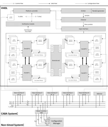
V. SYSTEMC/VHDLMIXEDVALIDATION
To validate our contribution we propose to analyze the config-uration infrastructure through a mixed SystemC/VHDL simulation model based on the platform presented in Section II. For this purpose, a complete Cycle and Bit Accurate SystemC [12] model of the proposed bus architecture was implemented. Then, this model was connected to a VHDL model of the multi-ASIP platform (which was already available) to allow a mixed SystemC/VHDL simulation. Finally, A non-timed SystemC model was developed to simulate the configuration manager (which is in charge of the configuration generation based on parameters set by the designer). The goal of this mixed model was to validate and to provide early evaluation of the proposed bus architecture through realistic configuration scenarios.
A. Platform model
Fig. 6 presents the different components implemented in the platform model. On the VHDL model side, A Random generator associated with an Emitter produce the encoded symbols. The channel model is an Additive White Gaussian Noise (AWGN). The Input interface distributes the received symbols in the
In-put memories of each DecASIP. A verification module compares
original symbols with decoded symbols to evaluate the decoding performance. Finally, A controller is used to manage the platform. In Fig. 6, data and control flow are highlighted with full black and broken lines respectively.
Non-timed SystemC Butterfly NoC N o C in te rfa ce N o C in te rfa ce NoCin te rf a ce N o C in te rf a ce DecASIP 0 DecASIP 2 Extrinsic Memory Program Memory Config Memory Input Memory
Cross metric Memory
DecASIP 1 Extrinsic Memory Program Memory Config Memory Input Memory
Cross metric Memory Extrinsic Memory Program Memory Config Memory Input Memory
Cross metric Memory
DecASIP 3 Extrinsic Memory Program Memory Config Memory Input Memory
Cross metric Memory
Input interface Channel Noisy symbols Emitter Symbols Random generator Platform controller Verification module To ASIPs To NoC Hard decision from ASIPs Config Memory CABA SystemC
Control flow Data flow Configuration flow
Mem.@ Data T_enable Dest. @ Selector Slave Interface 0 (SI_1) Slave Interface 1 (SI_3) Slave Interface N (SI_4) Slave Interface 0 (SI_0) Slave Interface 0 (SI_2) Master Interface (MI) T_init D_enable Data Base. @ Dest. @ Configuration Manager 26 8 8 26 8 8 VHDL
Figure 6. Architecture model for SystemC/VHDL mixed simulation
3 Frame n Frame n+1 t T(n) T(n+1) 2 1 Decoding Configuration
1 Configuration manager reads new frame parameters ; 2 configuration generation ; 3 Configuration transfer Frame n +2
3 2 1 Configuration for frame n+1 (configuration of the platform to deal with
the next frame)
Configuration for frame n+2
Figure 7. Configuration steps of the UDec platform
On the SystemC model side, 1 Selector and 5 SIs are imple-mented. Each SI is connected to a configuration memory: 4 De-cASIP configuration memories Conf. Mem. and one configuration memory associated with the controller of the platform. This last memory is used to configure the modules of the platform (see Section II-B). For clarity reasons, connections between the selector and the SIs are not represented in Fig. 6. The SystemC model of the Configuration Manager allows an interaction with the designer in order to simulate complete dynamic reconfiguration scenarios. In Fig. 6, Configuration data flow is shown in doted lines. B. Configuration scenario
In the context of this work, the maximum configuration latency of a frame is constrained by the previous frame decoding duration as shown in Fig. 1.a. The configuration of the UDec platform is divided in three steps as shown in Fig 7: (1) the configuration manager receives the configuration order associated with frame parameters (i.e. frame size, standard, throughput, targeted BER) necessary to generate the configuration for the DecASIPs. (2) the configuration parameters for each selected DecASIP presented in section II-B are generated. (3) the configuration parameters for each
Standard frame size Conf. time Dec. time Config. time
(in bits) (in cycles) (in cycles) ratio ( in %)
DVB-RCS 440 43 4528 0.95 DVB-RCS 1728 43 25548 0.17 3GPP-LTE 440 43 4751 0.91 3GPP-LTE 1728 43 26455 0.16 3GPP-LTE 3008 43 45215 0.095 Table II
CONFIGURATION LOADING IMPACT FOR4ACTIVEASIPS
selected DecASIP configuration memory is transfered through the configuration infrastructure presented in Section IV.
The SystemC/VHDL mixed model allows to rapidly evaluate several scenarios and to verify the efficiency of the platform. In order to illustrate one possible scenario and to evaluate the performance of our approach we consider in the next subsection a typical case study in which DVB-RCS and 3GPP-LTE frames are alternatively decoded. This scenario corresponds to the reception of TV (DVDB-RCS) and web browsing (3GPP-LTE) simultaneously on the same terminal.
C. Model evaluation
The proposed SystemC/VHDL mixed model allows a fast evalu-ation of the configurevalu-ation performance with respect to the decoding time for realistic configuration scenarios generated at run time by the configuration manager. The configuration latency of the UDec platform using the proposed approach is defined by equation 1.
Conf igurationLatency = 31 + (3.NASIP)
F (1)
Where NASIP is the number of DecASIPs and F is the
frequency of the proposed bus. 31 clock cycles are necessary to transfer the parameters common to all ASIPs and the parameters common to ASIPs of the same decoder component. 3 additional clock cycles are necessary to transfer parameters that are different for each ASIP.
Table II shows, for the two considered standards and for different data frame sizes, the ratio of the configuration loading regarding the decoding time for 4 active ASIPs and 6 decoding iterations. The last column represents the configuration time when compared to the total time required to configure and decode a frame. The configuration time is constant since the number of ASIPs is fixed. However, when the data frame size increases, the decoding time increases too. Consequently, the configuration time impact becomes negligible with high frame size (0.095% for a 3008-bit frame in 3GPP-LTE mode). When the frame size is smaller, the impact of configuration loading is still low (less than 1% for a 440-bit frame size).
The SystemC/VHDL mixed model has enabled an early and fast validation of the main features describes in Section IV. Starting from this model, next section presents the first hardware imple-mentation on FPGA and an evaluation for an ASIC technology.
VI. HARDWARE PROTOTYPE
To validate the proposed bus architecture and communication protocol presented in section IV a hardware prototype on a Xilinx XUPV5 platform based on a Virtex 5 LX110T FPGA was devel-oped.
Dest. @ Selector Slave Interface N (SI_4) Slave Interface 0 (SI_0) 8 26 8 D a ta M e m . @ W _ e n a b le 26 8 D a ta M e m . @ W _ e n a b le 26 8 D a ta M e m . @ W _ e n a b le 26 8 D a ta M e m . @ W _ e n a b le Slave Interface 1 (SI_3) Slave Interface 0 (SI_1) Slave Interface 0 (SI_2) 26 8 D a ta M e m . @ W _ e n a b le
Xilinx ChipScope Debug Module To computerVia JTAG
Mem.@ Data T_enable Dest. @ Master Interface (MI) 26 8 T_init D_enable Data Base. @ Dest. @ 26 8 8 FSL to MI Interface Asynchronous FIFO Microblaze FSL Timer UART PLB Local memory (BRAM) LMB
Figure 8. Architecture of the prototype
The prototype architecture is shown in Fig. 8. It consists of a Xilinx Microblaze soft core that generates the configuration at run-time. The configuration is then sent through an FSL bus to a FSL to MI interface. The Fast Simplex Link (FSL) [11] connection has been considered as this interconnect structure proposes a fast, simple and unidirectional connection for the Microblaze which ease its integration within the configuration infrastructure (other interconnection solution to the Microblaze would lead to an higher complexity and lower performance). An asynchronous FIFO is associated to the FSL connection in order to provide frequency domain flexibility on both Microblaze and configuration infrastruc-ture sides. The FSL to MI interface realizes the protocol adaptation between the FSL communication protocol and our bus protocol. Finally, the outputs of each SI are connected to a Xilinx ChipScope module that allows the run-time monitoring of these signals. This module replaces the configuration memories associated with the SIs.
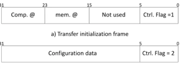
The FSL bus provides a solution to transfer, each cycle, a 32-bit width data. Hence, we define an adaptation protocol in order to, starting from a 32-bit frame, extract control and data information. Fig. 9 shows the two FSL frames model used to adapt the communication protocol. Depending of the control flag, the FSL to MI interface provides a transfer initialization or a data transfer service on the bus. Fig. 9.a shows the FSL frame model sent by the Microblaze to initialize a transfer on the bus. In this case the control flag is set to 1, the flag indicates that this frame corresponds to a transfer initialization. The 8-bit component destination and the 8-bit base memory address are extracted. One cycle later, the interfaces drives MI’s inputs as described in section IV-C. Fig. 9.b shows the FSL frame model sent by the Microblaze to transfer data after a transfer initialization. In this case the control flag is set to 2, the flag indicates that this frame corresponds to a data transfer. The 26-bit data is extracted from the frame and the interface drives MI’s inputs as described in section IV-C.
Thanks to this hardware implementation, configuration transfer time were evaluated for several numbers of DecASIPs. For this purpose, the Microblaze and the proposed bus frequency is set to 125 MHz. The Chipscope module is configured to monitor the output signals of the SIs. Table III shows the configuration transfer times of the bus compared to designs we have implemented using CoreConnect PLB4 [8] and AMBA AXI4 [7] buses connected to a Microblaze with the same clock frequency (set up to 125MHz). Thanks to the multicast mechanisms, a low overhead of 144 ns is
Ctrl. Flag =1
0 5
31 23 15
Comp. @ mem. @ Not used
Ctrl. Flag = 2 0 5 31 Configuration data a) Transfer initialization frame b) Data frame
Figure 9. FSL to MI protocol adaptation
Nb. Transfer latency (in ns) Speedup
ASIPs This work [8] [7] vs. [8] vs. [7]
4 1 032 3 872 2 212 3.75 2.14 6 1 176 5 808 3 168 4.94 2.69 8 1 320 7 744 4 224 5.87 3.2 16 1 896 15 488 8 448 8.17 4.45 32 3 048 30 976 16 896 10.16 5.54 64 5 352 61 952 33 792 11.57 6.31 Table III
CONFIGURATION TRANSFER TIME INns
necessary to configure each additional couple of DecASIPs (one ASIP in both natural and interleaved domains) while 1936 ns and 1056 ns are necessary for [8] and [7] respectively. Results of Table III show that the proposed implementation significantly reduces the configuration time overhead when the number of active DecASIPs increases compared to classical bus approaches.
Compared to equation 1, the performance of the proposed configuration infrastructure FPGA prototype is defined by equation 2.
Conf igurationLatency = 93 + (9.NASIP)
FM icroblaze (2)
Where NASIP is the number of DecASIPs and FM icroblaze is
the frequency of the Microblaze and the proposed bus. 93 clock cycles are necessary to transfer the parameters common to all ASIPs and the parameters common to ASIPs of the same decoder component. 9 additional clock cycles are necessary to transfer parameters that are different for each ASIP. Compared to equation 1, the performance penalty is due to two factors. Indeed, the FSL bus used to connect the Microblaze processor to the configuration infrastructure and the protocol adaptation between the FSL bus and the MI lead to additional cycles which impact the transfer latency. Moreover, the Microblaze doesn’t send one data per cycle on the FSL bus since several cycles are necessary to build the frames presented in Fig. 9 before each transfer.
However, as shown in Table III, using this solution combined with our low latency configuration infrastructure allows us to perform the configuration of up to 64 ASIPs in less than 10 µs (5.353 µs) which opens very interesting perspectives for future reconfigurable decoders.
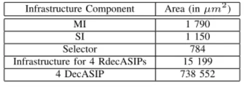
A logical synthesis of the proposed bus components was also done with a 65nm CMOS technology with a clock frequency objective equals to 500MHz. Table IV shows the area evaluation for the three components of the proposed configuration infrastructure. The logic overhead due to the configuration infrastructure is 0.015
mm2 which leads to a low area penalty of 2% regarding the
Infrastructure Component Area (in µm2)
MI 1 790
SI 1 150
Selector 784
Infrastructure for 4 RdecASIPs 15 199
4 DecASIP 738 552
Table IV
AREA OF THE PROPOSED CONFIGURATION ARCHITECTURE
Nb. Transfer latency (in ns) Speedup
ASIPs FPGA ASIC (estimated)
4 1 032 86 12 6 1 176 98 12 8 1 320 110 12 16 1 896 158 12 32 3 048 254 12 64 5 352 446 12 Table V
ESTIMATEDCONFIGURATION TRANSFER TIME INnsFOR ANASIC
IMPLEMENTATION
the selector is the lowest one since only a comparison with the input component address is necessary to know if the input vector has to be copied into the output or not. The complexity of the SI and MI components is quite similar. The difference is mainly due to the presence of a counter in the MI for incremental burst while 8-bit comparators is implemented in the SI for address comparison. Furthermore, considering an ASIC implementation with the frequency objective of 500 MHz, a significant speedup on the configuration transfer latencies shown in Table III can be expected compared to the 125 MHz FPGA prototype. Table V shows the estimated configuration transfer time for an ASIC implementation. Results are estimated using equation 1 with a bus frequency fixed to 500 MHz and show that a speedup of 12 can be reached compared to the FPGA implementation.
Results presented in this section show that the proposed con-figuration infrastructure offers an efficient solution for the UDec implementing up to 64 ASIPs. It guarantees configuration latency below 6µs providing a very low configuration latency overhead and meeting the configuration latency challenge as explained in the introduction. Furthermore, as detailed in Fig. 7, the next configuration computation and transfer is performed in parallel of the current data frame treatment. Such a solution meets future standard requirements where a code switch can be done as early as one data frame ahead [13].
VII. CONCLUSION
Configuration data transfer in application specific multiprocessor platforms is still an important challenge. In this paper, we propose a configuration infrastructure that provides an efficient and low complexity solution. This work was validated through a mixed VHDL/SystemC model and an FPGA prototype for timing and area evaluation. A synthesis targeting ASIC 65nm CMOS technology was also performed. Results show that configuration of a multi-ASIP platform implementing 64 multi-ASIPs can be achieved in 5.352 µs for an FPGA implementation. Future work targets the definition and the validation of decision algorithms to build an efficient self-adaptable multicore platform for turbo decoding in a dynamic environment.
REFERENCES
[1] P. Murugappa, R. Al-Khayat, A. Baghdadi, and M. J´ez´equel, “A Flexible High Throughput Multi-ASIP Architecture for LDPC and Turbo Decoding,” in Proc. of the Design, Automation and Test in Europe Conference & Exhibition (DATE), 2011.
[2] F. Clermidy, R. Lemaire, X. Popon, D. Ktenas, and Y. Thonnart, “An Open and Reconfigurable Platform for 4G Telecommuni-cation: Concepts and Application,” in Euromicro Conference on Digital System Design, Architectures, Methods and Tools, DSD ’09, aug. 2009, pp. 449 –456.
[3] C. Jalier, D. Lattard, G. Sassatelli, P. Benoit, and L. Torres, “Flexible and distributed real-time control on a 4G telecom MPSoC,” in Proc. of IEEE International Symposium on Circuits and Systems (ISCAS), 2010, pp. 3961 –3964.
[4] N. Ventroux, A. Guerre, T. Sassolas, L. Moutaoukil, G. Blanc, C. Bechara, and R. David, “Sesam: An mpsoc simulation envi-ronment for dynamic application processing,” in CIT, 2010, pp. 1880–1886.
[5] H. Moussa, A. Baghdadi, and M. Jezequel, “Binary de Bruijn on-chip network for a flexible multiprocessor LDPC decoder,” in Proc. of the Design Automation Conference (DAC), 2008, pp. 429–434.
[6] P. Robertson, P. Hoeher, and E. Villebrun, “Optimal and sub-optimal maximum a posteriori algorithms suitable for turbo decoding,” European Transactions on Telecommunications, vol. 8, no. 2, pp. 119–125, 1997.
[7] ARM, AMBA specifications v2.0. ARM. [Online]. Available: http://www.arm.com.
[8] IBM, CoreConnect Bus Architecture. IBM Microelectronics. [On-line]. Available: http://www.ibm.com/chips/products/coreconnect. [9] Altera, Avalon bus specification: Reference manual. Altera
Cor-poration. [Online]. Available: http://www.altera.com.
[10] Sonics network technical overview. Sonics, Inc. [Online]. Avail-able: http://www.sonicsinc.com.
[11] Xilinx, FSL V2.0 specification. Xilinx, Inc. [Online]. Available: http://www.xilinx.com.
[12] T. Grotker, System Design with SystemC. Norwell, MA, USA: Kluwer Academic Publishers, 2002.
[13] “IEEE Standard for Local and Metropolitan Area Networks Part 16: Air Interface for Fixed and Mobile Broadband Wireless,” IEEE Std 802.16e-2005, 2006.