HAL Id: hal-02107403
https://hal.archives-ouvertes.fr/hal-02107403
Submitted on 20 Nov 2019HAL is a multi-disciplinary open access archive for the deposit and dissemination of sci-entific research documents, whether they are pub-lished or not. The documents may come from teaching and research institutions in France or abroad, or from public or private research centers.
L’archive ouverte pluridisciplinaire HAL, est destinée au dépôt et à la diffusion de documents scientifiques de niveau recherche, publiés ou non, émanant des établissements d’enseignement et de recherche français ou étrangers, des laboratoires publics ou privés.
Guided Photoluminescence from Integrated
Carbon-Nanotube-Based Optical Waveguides
Loïc Bodiou, Qingyuan Gu, Maud Guezo, Enguerran Delcourt, Thomas
Batté, Jonathan Lemaitre, Nathalie Lorrain, Mohamed Guendouz, Hervé
Folliot, Joël Charrier, et al.
To cite this version:
Loïc Bodiou, Qingyuan Gu, Maud Guezo, Enguerran Delcourt, Thomas Batté, et al.. Guided Pho-toluminescence from Integrated Carbon-Nanotube-Based Optical Waveguides. Advanced Materials, Wiley-VCH Verlag, 2015, 27 (40), pp.6181-6186. �10.1002/adma.201502536�. �hal-02107403�
Guided photoluminescence from integrated carbon nanotubes-based optical waveguides
L. Bodiou1,*, Q. Gu1, M. Guézo1, E. Delcourt1, T. Batté1, J. Lemaitre1, N. Lorrain1, M. Guendouz1, H. Folliot1 and J. Charrier1, K.S. Mistry2,3, B.A. Larsen2 and J.L. Blackburn2, J.-L. Doualan4, A. Braud4 and P. Camy4
1 UMR FOTON, CNRS, Université de Rennes 1, INSA Rennes, Enssat, F22305, Lannion, France
2 National Renewable Energy Laboratory, Golden, Colorado 80401, United States
3 Department of Physics, University of Colorado, Boulder, Colorado 80309,
United States
4 Centre de Recherche sur les Ions, les Matériaux et la Photonique (CIMAP), UMR CEA-CNRS-ENSICaen, Université de Caen, Caen 14050, France
Abstract
We report the fabrication of planar and ridge waveguides made of semiconducting single-wall carbon nanotubes dispersed in fluorene-based polymers. Optical properties (refractive index, absorption and photoluminescence) of carbon nanotubes-incorporated polymer thin films are presented. Technological processing steps to obtain ridge waveguides are described and optical propagation at 1550 nm in these structures is confirmed by optical near field imaging of guided modes. Photoluminescence experiments on films and ridges waveguides are compared to demonstrate the guided photoluminescence of carbon nanotubes in the near infrared (1500-1600 nm).
Carbon nanotubes (CNT) and graphene exhibit outstanding mechanical, thermal, electronic and optical properties1,2,3. Graphene is attracting a growing interest of the scientific community and has been implemented as sensors4, photodetectors5,6 or transparent electrode in high efficiency solar cells7 and light emitting diodes8. Since graphene has no bandgap, this material is not expected luminesce from charge carriers relaxation, however graphene luminescence can be obtained by inducing a bandgap notably after oxygen plasma treatment9. The versatile CNT physical properties have also been widely investigated and numerous promising applications have emerged such as FET10, biomedical and gas sensors11,12.
Recently, a particular attention has been drawn to the implementation of CNT-based photonic devices. Nonlinear optical properties of CNT (notably the large and fast response of the real and imaginary parts of the third-order susceptibility) have found applications13 as saturable absorber for
mode-locked lasers14,15 and as nonlinear functional components (optical switch, signal converters or signal regenerator) for telecommunication systems16. Light-emitting devices based on electro- and photo-luminescence properties of semiconducting single-wall carbon nanotubes (s-SWCNT) have been developed17,18 and optical gain has been measured19. To overcome the relatively low quantum efficiency of SWCNT20, several studies have also been undertaken to couple SWCNT to optical cavities (Fabry-Perot planar cavity based on metallic or Bragg mirrors21,22, microring or microdisk resonators23,24 and photonic crystals25). The resulting luminescence enhancement factor can reach more than an order of magnitude.
SWCNT are usually synthesized as a blend that contain both metallic and semiconducting CNT species. As most optoelectronic applications require the solely use of s-SWCNT, the removal of metallic SWCNT and/or catalyst residues is therefore mandatory. To this end, several separation methods including density gradient ultracentrifugation26 (DGU), dielectrophoresis27 or extraction using aromatic polymers28 have been developed. To further increase their performance, some devices must also incorporate s-SWCNT with specific diameter and chirality. S-SWCNT that display spectral signature in the wavelength window around 1.55 µm would be for example highly desirable for devices dedicated to optical communications. The selective extraction of corresponding large-diameter (~1.3nm) s-SWCNT produced by laser vaporization (LV) has been demonstrated29,30 using polyfluorene-based polymers.
Recent studies have shown the possible integration of light emitting SWCNT onto waveguiding structures23,31,32. In that case, luminescence has to couple into the bus waveguide in order to be collected and this coupling efficiency has been estimated at 10 % and 50% in ref. 31 and 32 respectively. Despite appealing, the electrically-stimulated SWCNT light detected in ref. 32 is said also to originate predominantly from black-body radiation of metallic SWCNT rather than from excitonic transitions of s-SWCNT. To increase the efficiency of such devices, the incorporation of light-emitting s-SWCNT inside the waveguide could be an alternative approach. In this paper, we report the fabrication of planar and ridge waveguides of polymers containing selected chiralities of s-SWCNT in the guiding layer. The fabrication steps of these structures are compatible with CMOS processes and could therefore be integrated in silicon photonics technology. Optical characterizations are presented and guided photoluminescence in such structures is demonstrated.
SWCNT produced
by laser vaporization (LV) at 1125°C were dispersed with poly[(9,9-dihexyl fluorenyl-2,7-diyl)-co-(9,10-anthracene)] (PFH-A) in toluene at the concentration of XXX (to be confirmed by NREL). PFH-A has been shown to selectively wrapped large-diameter SWCNT29 and the resulting solution is
composed of narrow CNT chirality distributions consisting primarily of near-armchair semiconducting species. The growth temperature of the LV synthesis (1125°C) was chosen as it favors an enrichment in large-diameter s-SWCNT and particularly the (10,8) chirality whose S11 transition lies in the broadly used telecommunication wavelength window around 1.55 µm.
PFH-A/CNT films were deposited on different 1×1 cm2-substrates (Si, 5 µm-thick benzocyclobutene (BCB) on Si and 5 µm-thick thermally grown SiO2 on Si). For all these samples, the PFH-A/CNT solution (60µL) was spin-coated at low spin speed followed by hard baking under ambient atmosphere at 200°C for 5 minutes.
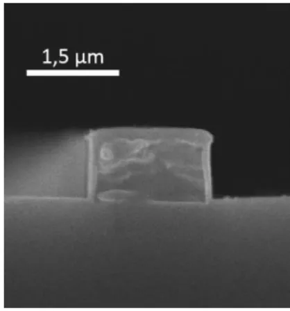
For ridge waveguide fabrication, the following additional processing steps were required. A thin SiO2 layer was first sputtered on the PFH-A/CNT film by plasma-enhanced chemical vapor deposition (Plassys MP550S) before Shipley S1805 photoresist spin-coating. The SiO2 layer acts as a protection layer and prevent any possible damage on the PFH-A/CNT film by the photoresist solvent. After soft-baking, a classical photolithographic process was then used for waveguide definition on a Süss Microtec MJB4 mask aligner. PFH-A/CNT ridge waveguides were patterned using the reactive ion etching (RIE) technique by exposing the layer to two successive SF6 and O2 plasmas at low pressure (Corial 300R reactive ion etching equipment). In situ monitoring of the dry etching was achieved by reflectometry. Figure 1 shows that vertical sidewalls are achieved with this procedure. Under the optimized etching conditions (125W, 10 mTorr, 25 sccm O2), no lateral undercuts are observed and the etch rate of the PFH-A/CNT film was typically around 100 nm/minute. A 100nm-thick SiO2 capping layer was finally sputtered to protect the PFH-A/CNT waveguides. The RMS roughness was measured at each stage of the technological process to reach ~15 nm after the second SiO2 protection layer sputtering.
Figure 1 : Scanning electron microscope image of a PFH-A/CNT ridge waveguide cross section after the SiO2 protection layer deposition on the CNT-based core layer.
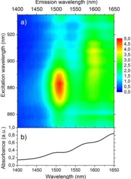
Photoluminescence (PL) measurements were performed on PFH-A/CNT films at room temperature using a continuous wave Ti:Sapphire laser (Coherent 890) as the excitation source and an optical spectrum analyzer (OSA - Ando AQ-6315E) for signal detection. The two-dimensional photoluminescence excitation (PLE) contour plot displayed in Figure 2 was generated by recording the PL spectra of the PFH-A/CNT film on Si as a function of the excitation wavelength. The excitation wavelength was tuned around the absorption energy of the S22 transition whereas luminescence was detected at wavelengths corresponding to the E11 transition. The PL spectra were recorded every 3 nm in the 845-935 nm wavelength range. This PLE map exhibit clear spectral signatures of near-armchair s-SWCNT species (10,8) and (10,9) and confirms that s-SWCNT with large diameters are extracted using PFH-A. Due to the sensitivity of SWCNT optical transition energies on their surrounding dielectric environment33, SWCNT excitation (S22) and emission (S11) energies in the film are slightly red shifted compared to those observed in toluene29 or assigned by Weisman et al.34.
Figure 2 : a) PLE map of a PFH-A/CNT film on Si, b) absorption of PFH-A/CNT film deposited on glass
Absorption spectrum of a PFH-A/CNT film on glass substrate in the near infrared region is displayed in Figure 2b. An extended absorption curve of PFH-A/CNT dissolved in toluene can be found in ref. 29. The three peaks observed in this spectrum around 1500, 1575 and 1650 nm correspond respectively to the S11 absorption energy of a few specific chiralities of s-SWCNT selected by PFH-A namely (10,8), (10,9) and (11,9) species. The luminescence of the latter s-SWCNT of (11,9) chirality cannot be seen on the PLE map displayed in Figure 2a. The (11,9) chirality s-SWCNT PL should have been observed around 1650 nm for an excitation wavelength of ~960 nm29 but was not be recorded
due to the detector bandwidth limitations and because the excitation wavelength was not tuned down to its E22 energy.
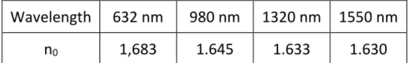
Refractive indexes of the PFH-A/CNT films were measured at different wavelengths (632, 980, 1320 and 1550nm) using the prism coupling technique on a Metricon 2010/M system. Using a two-parameter fitting procedure, this technique allows to simultaneously determine the refractive index and thickness of a film provided multimodal optical propagation in the film at the wavelength injected through the prism. As thick films were difficult to achieve due to the low viscosity of the PFH-A/CNT solution, multimodal behavior of the waveguide could only be achieved at 632 nm. Thicknesses obtained from the fitting procedure in the red part of the electromagnetic spectrum were therefore used as a fixed parameter to adjust the curves recorded in the infrared. These thicknesses were later confirmed by profilometry (Veeco Dektak 150 surface profiler) after the technological processing of ridge structures. M-lines measurements were performed on multiple locations on films deposited onto different substrates. The results are summarized in Table I. Refractive index uncertainties are below 5 × 10⁻³ at each wavelength and may be slightly higher than expected values for the M-lines technique due to the thinness of the film and film thickness and/or CNT loading non-uniformities.
Wavelength 632 nm 980 nm 1320 nm 1550 nm
n0 1,683 1.645 1.633 1.630
Table I : Linear refractive index (n0) of PFH-A/CNT films at different wavelengths
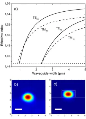
From these refractive index values, optical field distributions of the propagating modes and their corresponding effective indices were computed at 1550 nm for TE and TM polarizations as a function of the waveguide width using the film mode matching (FMM) method of a commercially available software (FIMMWAVE from Photon Design). These calculations were performed by considering a SiO2 lower cladding and a waveguide height of 1 µm corresponding to the spin-coated PFH-A/CNT film thickness surrounded by a 100 nm-thick SiO2 layer (nSiO2=1.446). From the simulated dispersion curves plotted in Figure 3a, it can be seen that the waveguide supports multimodal propagation for width larger than 2.3 µm for both TE and TM polarizations.
Figure 3 : a) Simulated effective indexes for the fundamental and first excited TE and TM modes as a function of waveguide width at λ=1.55µm. The solid and dashed lines correspond to TE and TM polarizations, respectively, the dotted line represents the SiO2 refractive index. b) Measured
near-field intensity mode profile of a 2 µm-wide ridge waveguide (the scale bar is 1µm) and c) Simulated intensity distribution of the TE00 mode for the same waveguide at a wavelength of 1550 nm.
Infrared light propagation was first demonstrated by in-coupling a 1.55 µm-broadband source using a microlensed fiber to ridge waveguides of different widths and imaging their output facet on an infrared camera (Hamamatsu C10633) through a high magnification and high numerical aperture microscope objective. The polarization was not controlled. Figure 3b shows the recorded near field pattern of the output light from a 2 µm-wide PFH-A/CNT ridge waveguide with a SiO2 lower cladding. It confirms the monomodal nature of propagation in the ridge structure for width smaller than 2µm. The mode diameters were measured to 2 × 1.5 μm2 (1/e2 intensity in horizontal and vertical directions respectively) in good agreement with the calculated value of 1.98 μm × 1.31 μm (Figure 3c)
To record guided luminescence from PFH-A/CNT ridge structure on SiO2 substrate, the camera was then replaced by a large core diameter multimode fiber connected to an OSA. To limit the region from which the PL could be collected and to prevent the detection of light scattered from the surface, a diaphragm and a long-pass filter were placed between the objective and the fiber. Alignment between waveguide output, objective and collecting fiber was then optimized. The guided PL measurements on ridge waveguides were performed at room temperature using a tunable
Ti:Sapphire laser operating between 850 and 935 nm. This laser beam was focused under normal incidence on the ridge top surface to obtain a spot size diameter of ~50µm at a distance of several hundreds of micrometers from the output facet.
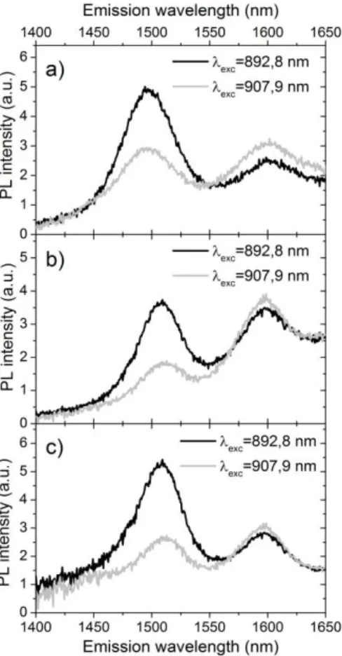
Figure 4 : a) guided PL spectra of 25 µm-wide PFH-A/CNT ridge waveguide excited at 892.8 and 907.9 nm, b) PL spectra of PFH-A/CNT films excited at the same wavelengths, c) Calculated guided
PL spectra from the PL spectra and absorption curve of PFH-A/CNT films
Figure 4a displays typical guided PL spectra from s-SWCNT with (10,8) and (10,9) chiralities in a 25 x 1 µm2 PFH-A/CNT ridge waveguide recorded for two different excitation wavelengths equal to 892.8 and 907.9 nm respectively. The spectra are corrected form the system response. However, significant differences in the relative intensities of the (10,8) and (10,9) s-SWCNT emission are clearly observed between the guided PL spectra and those obtained from the original films (Figure 4b). The ratio of peak PL intensities corresponding to the S11 transition of the (10,9) species (~1600nm) and the (10,8) chirality (~1500 nm) changes drastically between these two experiments. The reduction of the PL at longer wavelengths around 1600 nm is more pronounced comparatively to that of at shorter wavelengths. Waveguide losses arising from the technological processing cannot explain such differences between 1.5 and 1.6 µm. These changes of spectra shape can however be understood by taking into account the absorption spectra shown in Figure 2b. Indeed, as light emitted by the
s-SWCNT propagates towards the waveguide end, it is partly absorbed. As PFH-A/CNT absorption is higher at longer wavelengths, those will be more affected by the absorption through the propagation. To confirm this assumption, the PL spectra from PFHA-CNT films excited at 892.8 and 907.9 nm were divided by the absorption curve of PFH-A/CNT films (Figure 4c). The very similar shape of the resulting spectra with those recorded during guided PL experiments (Figure 4a) is a clear indication that s-SWCNT luminescence has effectively been guided in the ridge structure.
Fabrication process of planar and ridge waveguides made of s-SWCNT dispersed in fluorene-based polymers on different substrates have been described. Absorption and PL measurements on thin films incorporating selected s-SWCNT were measured. Guiding properties of PFH-A/CNT ridge waveguides at 1550 nm were simulated and compared with a good agreement to experimental near-field imaging of optical modes propagating in the structure. Guided PL at telecommunication wavelengths from specific chiralities s-SWCNT is demonstrated and shows the potential applications of this material for future integrated active photonic circuits based on carbon nanotubes.
This work was supported by the Région Bretagne, Lannion Trégor Communauté, the European Regional Development Fund and the French Ministry of Research
1 Michele T. Byrne and Yurii K. Gun’ko, “Recent Advances in Research on Carbon Nanotube–Polymer
Composites”, Adv. Mat., 21, 1 (2009).
2 F. Bonaccorso, Z. Sun, T. Hasan & A. C. Ferrari, “Graphene photonics and optoelectronics” Nat. Photonics 4,
611 (2010).
3 Phaedon Avouris, Marcus Freitag and Vasili Perebeinos, “Carbon-nanotube photonics and optoelectronics”,
Nat. Photonics, 2, 341 (2008).
4 Yuyan Shao, Jun Wang, Hong Wu, Jun Liu, Ilhan A. Aksay, Yuehe Lin, “Graphene Based Electrochemical Sensors
and Biosensors: A Review”, Electroanal, 22, 1027 (2010).
5 F. Xia, T. Mueller, Y.-M. Lin, A. Valdes-Garcia, and P. Avouris, “Ultrafast graphene photodetector”, Nat.
Nanotechnol., 4, 839 (2009).
6 Marco Furchi, Alexander Urich, Andreas Pospischil, Govinda Lilley, Karl Unterrainer, Hermann Detz, Pavel
Klang, Aaron Maxwell Andrews, Werner Schrenk, Gottfried Strasser, and Thomas Mueller, “Microcavity-Integrated Graphene Photodetector”, Nano Lett., 12, 2773 (2012).
7 Zongyou Yin, Jixin Zhu, Qiyuan He, Xiehong Cao, Chaoliang Tan, Hongyu Chen, Qingyu Yan, and Hua Zhang,
“Graphene-Based Materials for Solar Cell Applications “, Adv. Energy Mater., 4, 1300574 (2014).
8 Tae-Hee Han, Youngbin Lee, Mi-Ri Choi, Seong-Hoon Woo, Sang-Hoon Bae, Byung Hee Hong, Jong-Hyun Ahn
and Tae-Woo Lee, “Extremely efficient flexible organic light-emitting diodes with modified graphene anode”, Nat. Photonics, 6, 105 (2012).
9 T. Gokus, R. R. Nair, A. Bonetti, M. Böhmler, A. Lombardo, K. S. Novoselov, A. K. Geim, A. C. Ferrari, and A.
10 R. Martel, T. Schmidt, H.R. Shea, T. Hertel, P. Avouris, P, “Single- and multi-wall carbon nanotube field-effect
transistors”, Appl. Phys. Lett., 73, 2447 (1998).
11 Sebastian Kruss, Andrew J. Hilmer, Jingqing Zhang, Nigel F. Reuel, Bin Mu, Michael S. Strano, “Carbon
nanotubes as optical biomedical sensors”, Adv. Drug. Deliver. Rev., 65, 1933 (2013).
12 Jing Li, Yijiang Lu, Qi Ye, Martin Cinke, Jie Han, and M. Meyyappan, “Carbon Nanotube Sensors for Gas and
Organic Vapor Detection”, Nano Lett., 3, 929 (2003).
13 Shinji Yamashita, “A Tutorial on Nonlinear Photonic Applications of Carbon Nanotube and Graphene”, J.
Lightwave Technol., 30, 427 (2012).
14 S. Yamashita, Y. Inoue, S. Maruyama, Y. Murakami, H. Yaguchi, M. Jablonski, and S. Y. Set, “Saturable
absorbers incorporating carbon nanotubes directly synthesized onto substrates and fibers and their application to mode-locked fiber lasers”, Opt. Lett., 29, 1581 (2004).
15 Tawfique Hasan, Zhipei Sun, Fengqiu Wang, Francesco Bonaccorso, Ping Heng Tan, Aleksey G. Rozhin, and
Andrea C. Ferrari, “Nanotube–Polymer Composites for Ultrafast Photonics”, Adv. Mater., 21, 3874 (2009).
16 K. K. Chow, S. Yamashita, and S. Y. Set, “Four-wave-mixing-based wavelength conversion using a
single-walled carbon-nanotube- deposited planar lightwave circuit waveguide”, Opt. Lett., 35, 2070 (2010).
17 Megumi Kinoshita, Mathias Steiner, Michael Engel, Joshua P. Small, Alexander A. Green, Mark C. Hersam,
Ralph Krupke, Emilio E. Mendez, and Phaedon Avouris, “The polarized carbon nanotube thin film LED“, Opt. Express, 18, 25738 (2010).
18 Sheng Wang, Qingsheng Zeng, Leijing Yang, Zhiyong Zhang, Zhenxing Wang, Tian Pei, Li Ding, Xuelei Liang,
Min Gao, Yan Li, and Lian-Mao Peng, “High-Performance Carbon Nanotube Light-Emitting Diodes with Asymmetric Contacts”, Nano Lett., 11, 23 (2011).
19 E. Gaufrès, N. Izard, X. Le Roux, D. Marris-Morini, S. Kazaoui, E. Cassan & L. Vivien, “Optical gain in carbon
nanotubes”, Appl. Phys. Lett., 96, 231105 (2010).
20 Dmitri A. Tsyboulski, John-David R. Rocha, Sergei M. Bachilo, Laurent Cognet, and R. Bruce Weisman,
“Structure-Dependent Fluorescence Efficiencies of Individual Single-Walled Carbon Nanotubes”, Nano Lett., 7, 3080 (2007).
21 D. Legrand, C. Roquelet, G. Lanty, Ph. Roussignol, X. Lafosse, S. Bouchoule, E. Deleporte, C. Voisin, and J. S.
Lauret, “Monolithic microcavity with carbon nanotubes as active material”, Appl. Phys. Lett., 102, 153102 (2013).
22 Etienne Gaufrès, Nicolas Izard, Xavier Le Roux, Saïd Kazaoui, Delphine Marris-Morini, Eric Cassan, and Laurent
Vivien, “Optical microcavity with semiconducting single-wall carbon nanotubes”, Opt. Express, 18, 5740 (2010).
23 S. Imamura, R. Watahiki, R. Miura, T. Shimada, and Y. K. Kato, “Optical control of individual carbon nanotube
light emitters by spectral double resonance in silicon microdisk resonators”, Appl. Phys. Lett., 102, 161102 (2013).
24 Adrien Noury, Xavier Le Roux, Laurent Vivien and Nicolas Izard, “Controlling carbon nanotube
photoluminescence using silicon microring resonators”, Nanotechnology, 25, 215201 (2014).
25 R. Watahiki, T. Shimada, P. Zhao, S. Chiashi, S. Iwamoto, Y. Arakawa, S. Maruyama, and Y. K. Kato,
“Enhancement of carbon nanotube photoluminescence by photonic crystal nanocavities”, Appl. Phys. Lett., 101, 141124 (2012).
26 Saunab Ghosh, Sergei M. Bachilo and R. Bruce Weisman, “Advanced sorting of single-walled carbon
nanotubes by nonlinear density-gradient ultracentrifugation”, Nat. Nanotechnol., 5, 443 (2010).
27 Ralph Krupke, Frank Hennrich, Hilbert v. Löhneysen, Manfred M. Kappes, “Separation of Metallic from
Semiconducting Single-Walled Carbon Nanotubes”, Science, 301, 344 (2003).
28 Adrian Nish, Jeong-Yuan Hwang, James Doig and Robin J. Nicholas, “Highly selective dispersion of
29 Kevin S. Mistry, Brian A. Larsen and Jeffrey L. Blackburn, “High-Yield Dispersions of Large-Diameter
Semiconducting Single-Walled Carbon Nanotubes with Tunable Narrow Chirality Distributions”, ACS Nano, 7, 2231 (2013).
30 Nicolas Berton, Fabien Lemasson, Angela Poschlad, Velimir Meded, Frank Tristram, Wolfgang Wenzel, Frank
Hennrich, Manfred M. Kappes, and Marcel Mayor, “Selective Dispersion of Large-Diameter Semiconducting Single-Walled Carbon Nanotubes with Pyridine-Containing Copolymers”, Small, 10, 360 (2014).
31 Etienne Gaufrès, Nicolas Izard, Adrien Noury, Xavier Le Roux, Gilles Rasigade, Alexandre Beck, and Laurent
Vivien, “Light Emission in Silicon from Carbon Nanotubes”, ACS Nano, 6, 3813 (2012).
32 S. Khasminskaya, F. Pyatkov, Be. S. Flavel, W. H. Pernice & R. Krupke, “Waveguide-Integrated Light-Emitting
Carbon Nanotubes”, Adv. Mater., 26, 3465 (2014).
33 Brian A. Larsen, Pravas Deria, Josh M. Holt, Ian N. Stanton, Michael J. Heben, Michael J. Therien and Jeffrey L.
Blackburn, “Effect of Solvent Polarity and Electrophilicity on Quantum Yields and Solvatochromic Shifts of Single-Walled Carbon Nanotube Photoluminescence”, J. Am. Chem. Soc., 134, 12485 (2012).
34 R. Bruce Weisman and Sergei M. Bachilo, “Dependence of Optical Transition Energies on Structure for