HAL Id: hal-02318716
https://hal.telecom-paris.fr/hal-02318716
Submitted on 17 Oct 2019
HAL is a multi-disciplinary open access
archive for the deposit and dissemination of
sci-entific research documents, whether they are
pub-lished or not. The documents may come from
teaching and research institutions in France or
abroad, or from public or private research centers.
L’archive ouverte pluridisciplinaire HAL, est
destinée au dépôt et à la diffusion de documents
scientifiques de niveau recherche, publiés ou non,
émanant des établissements d’enseignement et de
recherche français ou étrangers, des laboratoires
publics ou privés.
Characterization at Logical Level of Magnetic Injection
Probes
Oualid Trabelsi, Laurent Sauvage, Jean-Luc Danger
To cite this version:
Oualid Trabelsi, Laurent Sauvage, Jean-Luc Danger. Characterization at Logical Level of Magnetic
Injection Probes. 2019 Joint International Symposium on Electromagnetic Compatibility and
Asia-Pacific International Symposium on Electromagnetic Compatibility, Jun 2019, Sapporo, Japan.
�hal-02318716�
Characterization at Logical Level of Magnetic
Injection Probes
Oualid Trabelsi, Laurent Sauvage and Jean-Luc Danger
LTCI, T´el´ecom ParisTech, Institut Polytechnique de Paris Saclay, France
Email: [email protected]
Abstract—Intentional electromagnetic interference is an ef-fective mean to jeopardize the security of integrated circuits. In this paper, we propose a new approach to evaluate the efficiency of magnetic probes used to radiate a disturbance: measuring its impact within the target of the attack, more precisely on the propagation delay of a combinational path. The characterization of five probes carried out using three different integrated circuits is reported. In all cases, bespoke, handmade probes outperform commercial ones. Experimental results also show that the electromagnetic coupling between the probes and the integrated circuits is mainly due to global, bonding wires.
Index Terms—Side-channel attacks, immunity testing, probes, field programmable gate array.
I. INTRODUCTION
Immunity to electromagnetic interference is a well-studied problem, and numerous solutions have been proposed to guarantee the proper functioning of electronic equipment. However, applying interference with a level much higher than those defined in Electromagnetic compatibility (EMC) standards has been demonstrated as an effective mean to corrupt the security of cyber-physical systems [1]. For instance, an Electromagnetic fault injection (EMFI) while an Integrated circuit (IC) is processing a wrong PIN code may turn it into a right one.
The success of an EMFI largely depends on the properties (e.g., the number of turns) of the probe which generates the radiated disturbance [6]. Designing and characterizing such antenna is a very old research topic [5]. When it comes to deal with EMC of IC, the International Electrotechnical Commission recommends to use magnetic probes, and to assess their efficiency by measuring the spatial distribution of the near field strength in the vicinity of a microstrip line [4]. However, the efficiency of an EMFI is related to the occurrence of exploitable faults within the IC, and there is no obvious relationship with the strength of the disturbing field. Therefore, in order to compare injection probes, we propose to observe the impact of EMFI at logical level, i.e. on logic gates of a victim IC.
Our method is described in section II, and the five magnetic probes used for the characterizations in section III. Section IV presents the experimental results, and section V draws conclu-sions and provide perspectives.
This research is financially supported by the “Fonds Unique Intermin-ist´eriel” (FUI, French Government) through the CSAFE+ program.
II. CHARACTERIZATION ATLOGICALLEVEL
Faults in an IC are created by EMFI either directly when the logic state of some storage elements such as flip-flops is inverted, or when the propagation delay of some combinational paths is so increased that their output is stored while the right value is not arrived [6]. These previous works have focused on the impact of EMFI on a large chain of flip-flops. In a complementary way, our method involves a large cascade of combinational logic gates, whose nominal propagation delay is denoted by tp. Under EMFI, this delay is subject to variations,
and we define its measurements as t0p. Therefore, at a position
(x, y) of the probe, the impact ∆tp(x, y) can be evaluated as
the difference between t0p(x, y) and tp.
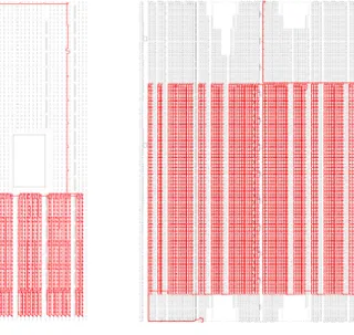
The test design has been implemented as a cascade of buffers, programmed in a reconfigurable IC, namely Field-programmable gate array (FPGA). For the sake of generality, the characterizations have been achieved on three different FPGAs: A Microsemi SmartFusion2 manufactured in 65 nm process technology, a 90 nm Xilinx Virtex-II Pro and a 45 nm Xilinx Spartan-6. The propagation delay of a single buffer depends on the process technology, and the propagation delay of the whole cascade is a multiple of the number of buffers. The corresponding values for each FPGA are reported in table I. The placement of the design has been constrained to the bottom part of the FPGA, as visible in the floorplans of fig. 1. In this way, it is possible to check whether there is a correlation between the impact of an EMFI and the position of the injection probe.
Table I
PARAMETERS OF THECASCADE OFBUFFERS, ACCORDING TO THEFPGA
FPGA Process #Buffers tp
(nm) (µs) Microsemi SmartFusion2 65 5000 0.97 Xilinx Virtex-II Pro 90 5888 2.23 Xilinx Spartan-6 45 4096 1.78
Figure 2 is the timings diagram of the EMFI: At tin, the
input signal of the test design is fliped to the high logic state. The signal arrives at the output at time tout, or at t0out when
an EMFI impacts the nominal propagation delay tp by ∆tp.
The figure illustrates a positive impact, which corresponds to a deceleration of the propagation, but experiment also shows
(a) Microsemi SmartFusion2 (b) Xilinx Virtex-II Pro (c) Xilinx Spartan-6 Figure 1. Floorplan of the cascade of buffers, according to the FPGA.
that the impact can be negative (t0out < tout), meaning an
acceleration of the propagation. In both cases, the EMFI has to occur during the propagation, i.e. between tinand t0out. Indeed,
a modification of the propagation delay while the output has been updated is unobservable. As t0out is not known a priori, we add some margins: The EMFI starts at time tinj > tin, and
consists of successive pulses, distant from 3 ns, and numerous enough to cover the injection window iw which ends before
t0out. Note that as the nominal propagation delay is different
for each FPGA, the width of the injection window is adjusted accordingly: 375 ns for Microsemi SmartFusion2, 1200 ns for Xilinx Virtex-II Pro and 1020 ns for Xilinx Spartan-6. A single pulse has a rising and falling edge of 1 ns, hence a width of 1.5 ns.
Figure 2. EMFI timings diagram.
The propagation delay between the rising edge of the input signal and that of the output signal is measured using an internal function of the oscilloscope. The rest of the EMFI test bench is very similar to that of [1, fig. 1]: A 330 MHz pulse generator, whose output amplitude is set up to 0 dBm, driving a 10 kHz to 400 MHz 260 W class A broadband amplifier. The
magnetic probe to characterize is connected to its output, and moved over a FPGA using a 4-axis positioning system.
III. MAGNETICINJECTIONPROBES
We have characterized the impact at logical level of five magnetic injection probes, whose mechanical parameters are presented in table II.
Langer RF-B 3-2 [3] (fig. 3a) is a Commercial off-the-shelf (COTS) probe, designed for the measurement of Printed circuit board (PCB) emission in the frequency range from 30 MHz to 3 GHz. As it is a passive component, we can operate it in a reverse way, hence for EMFI. The datasheet indicates a head diameter Φh of 4 mm, and from X-ray radiography, we have
identified it is an air-core probe, made of two turns of a wire with a diameter Φw of 80 µm.
Langer BS 05DB-h [2] (fig. 3b) is also a COTS probe, but dedicated to PCB immunity (magnetic field source), and as such, designed to resist high voltage up to 4.4 kV. X-ray radiography reveals it is also an air-core probe, but with seven turns of a 100 µm wire, forming a coil with a diameter of 2 mm.
Table II
MECHANICALPARAMETERS OF THEMAGNETICINJECTIONPROBES
Probe reference Φh Φw #Turns Core
(mm) (µm) Langer RF-B 3-2 [3] 4 80 2 Air Langer BS 05DB-h [2] 2 100 7 Air LIRMM F [6] 0.75 200 7 Fe Arelis N1 0.80 150 4 Fe Arelis S7-T 0.75 200 4 Fe
(a) Langer RF-B 3-2 (b) Langer BS 05DB-h (c) LIRMM F (d) Arelis N1 (e) Arelis S7-T Figure 3. Photographs of the magnetic probes.
(a) Langer RF-B 3-2 (b) Langer BS 05DB-h (c) LIRMM F (d) Arelis N1 (e) Arelis S7-T Figure 4. Spatial distribution of ∆tpon Microsemi SmartFusion2, according to magnetic probes.
(a) Langer RF-B 3-2 (b) Langer BS 05DB-h (c) LIRMM F (d) Arelis N1 (e) Arelis S7-T Figure 5. Spatial distribution of ∆tpon Xilinx Virtex-II Pro, according to magnetic probes.
(a) Langer RF-B 3-2 (b) Langer BS 05DB-h (c) LIRMM F (d) Arelis N1 (e) Arelis S7-T Figure 6. Spatial distribution of ∆tpon Xilinx Spartan-6, according to magnetic probes.
LIRMM F probe (fig. 3c) is the handmade flat injector described in [6, §2.2]. It is composed of seven turns of a 200 µm wire around a 0.75 mm ferrite core.
The two last probes are prototypes developed by the french company Arelis, built from a ferrite core whose shape is that of a circular truncated cone, with a top diameter of 1.5 mm. The bottom diameter equals 0.80 mm for Arelis N1 (fig. 3d) and 0.75 mm for Arelis S7-T (fig. 3e). Arelis N1 is an handmade probe, composed of four turns of a 150 µm wire.
Arelis S7-T (fig. 3e) is an industrial version of Arelis N1: The coil winding is manufactured by layering three small PCBs, with a 200 µm copper path. The coil shape is therefore a square. Furthermore, to improve the impedance matching, an RF transformer with an impedance ratio of 2:1 has been added.
IV. EXPERIMENTALRESULTS
The experimental results reported in this section correspond to the spatial distribution of ∆tp for each FPGA and probe.
For a given position (x, y), the propagation delay, with or without EMFI, is evaluated as the arithmetic mean of ten measurements. For each FPGA, 40 × 40 positions at a distance (z-axis) of 50 µm from their package have been considered. It represents a square area of 19.4 mm × 19.4 mm for Microsemi SmartFusion2 (figs. 4 and 7a), 24.0 mm × 24.0 mm for Xilinx Virtex-II Pro (fig. 5), and 18.0 mm × 18.0 mm for Xilinx Spartan-6 (fig. 6). The best probe for EMFI on combinational logic is expected to have a maximal positive impact on ∆tp1,
exclusively on the logic gates carrying sensitive data, as those
in the neighbouring may belong to some EMFI detectors. In other words, the probe should have a high spatial resolution.
For Microsemi SmartFusion2, the probe fitting the best these criteria is LIRMM F (fig. 4c), with a maximal positive impact of 3 ns. Its spatial distribution contains large areas because the probe is coupling with elements of a size much greater than its spatial resolution. A sound way to estimate this latter is focusing on the sharpness of the spatial distribution, i.e. on the width of the border (typically in white color) from one area with a given impact to an other one. Arelis probes (figs. 4d and 4e) come at the second place, with an identical sharpness but a lower impact, and finally Langer probes (figs. 4a and 4b), with a low impact and blurred borders.
This ranking is consistent with the mechanical parameters of the probes (table II): LIRMM F and Arelis probes feature a better spatial resolution than Langer probes thanks to their core which has first a smaller diameter, second a greater magnetic permeability, and in consequence a higher flux density. And since LIRMM F has a winding with almost two times more turns than that of Arelis probes, it additionally has a better impact.
(a) (b)
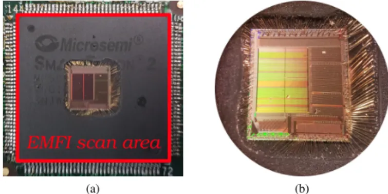
Figure 7. Microsemi SmartFusion2 with its package decapsulated in the center (a), revealing the silicon die (b).
Whatever the probe, from a macroscopic point of view, all spatial distributions (fig. 4) follow an identical star shape: In the center, the impact is very low, and all around, in a circular way, it alternates between deceleration (in red) then acceleration (in blue) areas. On another side, the logic gates are implemented within the silicon die of the FPGA, which is located in the center of the package (fig. 7). We thus conclude that EMFI does not directly impact the FPGA’s core, but rather the bonding wires, probably these of the power rails.
For Xilinx Virtex-II Pro, the maximal positive impact equals 10 ns, and is reported for Langer BS 05DB-h (fig. 5b). It is three times greater than the impact on Microsemi SmartFusion2. We assume that this is due to the process technology: 90 nm for the former versus 65 nm for the latter. The layering method of each technology has also to be considered. As previously, the deceleration (in red) areas located at the top and at the
bottom of the distribution are certainly due to a coupling with bonding wires. If we seek to have an impact solely on the FPGA’s core, i.e. in the center, then LIRMM F remains the best probe.
Finally, for Xilinx Spartan-6, 10 ns of maximal positive impact are possible using Arelis S7-T (fig. 6e). Nevertheless, the results for LIRMM F, the best probe so far, are very similar (fig. 6c). Unlike previous characterizations, there is no visible coupling with bonding wires. They must be absent from the package, which should use flip chip technology.
V. CONCLUSIONS& PERSPECTIVES
We proposed in this paper to characterize EMFI probes regarding their potential to create faults within an IC by increasing of propagation delays. In other words, we propose to include into the characterization the electromagnetic coupling between the probe and the IC target of EMFI. For a given FPGA, experimental results are quasi identical, which means this coupling does not really matter. At the opposite, they are really different for each FPGA, depending on the coupling with some elements such as bonding wires. The ranking of the probes is consistent with the theory of electromagnetism: A core with a small diameter and a high magnetic permeability, e.g. ferrite, leads to high resolution probe, and a winding with a high number of turns increases the strength of the magnetic field, hence the impact.
As future works, we propose to investigate whether various placement constraints for the design, i.e. placed at the top and bottom half of the FPGA, induce a different impact. We also plan to repeat the same characterization, but by changing some parameters of the electromagnetic disturbance: amplitude, injection time, number of pulses, frequency, polarity, etc.
REFERENCES
[1] Amine Dehbaoui, Jean-Max Dutertre, Bruno Robisson, and Assia Tria. Electromagnetic transient faults injection on a hardware and a software implementations of AES. In Guido Bertoni and Benedikt Gierlichs, editors, 2012 Workshop on Fault Diagnosis and Tolerance in Cryptography, Leuven, Belgium, September 9, 2012, pages 7–15. IEEE Computer Society, 2012. [2] Langer EMV-Technik. BS 05DB-h magnetic field source. https://www.langer-emv.com/en/product/accessory-eft-burst-generators- iec-61000-4-4/15/h2-set-field-sources/874/bs-05db-h-magnetic-field-source/60.
[3] Langer EMV-Technik. RF-B 3-2 h-field probe 30 MHz up to 3 GHz. https://www.langer-emv.com/en/product/rf-passive-30-mhz-3-ghz/35/rf2- set-near-field-probes-30-mhz-up-to-3-ghz/272/rf-b-3-2-h-field-probe-30-mhz-up-to-3-ghz/15.
[4] International Electrotechnical Commission (IEC). IEC/TS 61967-6, Integrated circuits – Measurement of electromagnetic emissions, 150 kHz to 1 GHz – Part 6: Measurement of conducted emissions – Magnetic probe method, June 2008.
[5] J.D. Kraus. Antennas. McGraw-Hill electrical and electronic engineering series. McGraw-Hill, 1950.
[6] S´ebastien Ordas, Ludovic Guillaume-Sage, Karim Tobich, Jean-Max Dutertre, and Philippe Maurine. Evidence of a Larger EM-Induced Fault Model. In Marc Joye and Amir Moradi, editors, Smart Card Research and Advanced Applications - 13th International Conference, CARDIS 2014, Paris, France, November 5-7, 2014. Revised Selected Papers, volume 8968 of Lecture Notes in Computer Science, pages 245–259. Springer, 2014.