HAL Id: hal-00938964
https://hal.archives-ouvertes.fr/hal-00938964
Submitted on 29 Jan 2014
HAL is a multi-disciplinary open access
archive for the deposit and dissemination of
sci-entific research documents, whether they are
pub-lished or not. The documents may come from
teaching and research institutions in France or
abroad, or from public or private research centers.
L’archive ouverte pluridisciplinaire HAL, est
destinée au dépôt et à la diffusion de documents
scientifiques de niveau recherche, publiés ou non,
émanant des établissements d’enseignement et de
recherche français ou étrangers, des laboratoires
publics ou privés.
3D MPSoC Design Using 2D EDA tools: Analysis of
Parameters
Mohammad Jabbar, A. M’Zah, Omar Hammami, Dominique Houzet
To cite this version:
Mohammad Jabbar, A. M’Zah, Omar Hammami, Dominique Houzet. 3D MPSoC Design Using 2D
EDA tools: Analysis of Parameters. DATE 2013 - Design, Automation and Test in Europe, Mar 2013,
Grenoble, France. pp.1-2. �hal-00938964�
3D MPSoC Design Using 2D EDA tools: Analysis of Parameters
M. H. Jabbar
1,2, A. M’zah
2, O. Hammami
2, D. Houzet
11
GIPSA-Lab, Grenoble INP
2
ENSTA Paristech
Abstract – Design space exploration of 3D MPSoC
architecture is reported in this paper analyzing the impact of 2D EDA tools to the 3D architecture performance. In particular, we study how 3D performance is varied when changing the EDA tools options intending to highlight design issues of 3D design. Results show that 3D timing performance is affected greatly compared with power consumption and total wirelength.
I. Introduction and Related Works
The number of processing elements will continue to increase in the coming years as projected by ITRS and interconnect is one of the important design problems that reduces the benefits of traditional CMOS scaling method at each generation. 3D integration has become the alternative technology to continue producing higher performance and capacity electronic devices through its short and high density of vertical interconnect using through silicon via (TSV). Design space exploration is one of the important things to be concerned helping designers to evaluate different possible design implementations before it is implemented in real hardware and is particularly important for 3D architecture to be able to choose the architectural candidate with the most performance gain.
A limited number of works have been reported with regards to the design space exploration of 3D architecture. System level design space exploration for 3D architecture is proposed by [1] enabling exploration of different stacking and partitioning schemes and their affect on the performance, power and temperature. Another design space exploration for 3D stacked architecture is presented in [2] [3] focusing different 3D packaging solutions with logic and memory integration. Design space exploration of 3D architecture focusing on microprocessor and memory architecture is presented in [4]. Our previous work of 3D design space exploration is limited to only single tier and thus does not sufficient to have a complete analysis [5].
Differs from the previous reported works, this study perform design space exploration of 2D EDA tools parameters on the 3D architecture. We have chosen different placement and routing options in SoC Encounter and evaluate their impact on the timing slack, power consumption and wirelength of the 3D architecture. Due to the unavailability of 3D design tools capable of doing 3D synthesis, 3D placement, 3D CTS and 3D routing, designing using 2D EDA tools is the only solution. The aim of this study is to
analyze how 2D EDA tools are affecting the overall 3D architecture performance since it will not be an issue when using a true 3D design tool. We have extended our previous work by integrating a complete 3D design exploration flow to get more accurate results and analysis.
II. Design Space Exploration
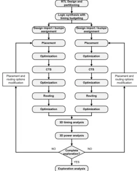
Our 3D design is based on Tezzaron 3D technology which is a two-tier face-to-face bonding using microbump for the inter-tier connection (Figure 2) [6]. Figure 1 shows the design flow used in this work to explore placement and routing options in the place and route tool. Synopsys Design Compiler was used for the logic synthesis while Cadence SoC Encounter was used for place and route of both tiers that run in parallel during the exploration. 3D timing analysis and power analysis was done using Synopsys PrimeTime and PrimePower tool. The design space exploration is conducted using a script that automatically modifies the EDA tool options at each iteration.
RTL Design and partitioning Logic synthesis with
timing budgeting Placement Optimization CTS 3D power analysis 3D timing analysis Placement Optimization CTS Placement and routing options modification Placement and routing options modification
Design import / bumps assignment Design import / bumps
assignment Exploration analysis Complete exploration? YES NO NO Optimization Optimization Optimization Optimization Routing Routing
Figure 1: Design flow for 3D design space exploration
Figure 2: MPSoC1: 3D 2 Tiers 16PE Mesh Topology
The selected options of EDA tool as shown in Table 1 have been chosen based on its properties that strongly effect the quality of final netlist for 2D design and thus make it more important to evaluate it in the 3D design.
III. Resuts and Discussion
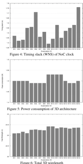
The results of the exploration are shown from Figure 3 to Figure 6 for timing slack, power and wirelength of the 3D architecture. It can be seen from the figures that the timing slack for both NoC and processor is varied substantially between each exploration while for power consumption as well as total wirelength does not varied very much. The reason is because we have chosen timing driven option for both placement and routing and power driven is only explored at placement stage.
Table 1: EDA tool options for the exploration
Placement options Routing options Design ID Timing Driven Power Driven Timing Driven Route Timing Driven Effort 1 False False False 5 2 False False False 10 3 False False True 5 4 False False True 10 5 False True False 5 6 False True False 10 7 False True True 5 8 False True True 10 9 True False False 5 10 True False False 10 11 True False True 5 12 True False True 10 13 True True False 5 14 True True False 10 15 True True True 5 16 True True True 10
Figure 3: Timing slack (WNS) of processor clock
Figure 4: Timing slack (WNS) of NoC clock
Figure 5: Power consumption of 3D architecture
Figure 6: Total 3D wirelength
IV. Conclusion
We have presented a design space exploration of 3D MPSoC architecture to evaluate the impact of 2D EDA tool on its performance such as timing slack, power and wirelength. The results suggest that 3D timing performance is varied widely than power consumption and total wirelength.
References
[1] S. Priyadarshi, J. Hu, W. H. Choi, S. Melamed, X. Chen, W. R. Davis, and P. D. Franzon, “Pathfinder 3D: A flow for system-level design space exploration,” in
3D Systems Integration Conference (3DIC), 2011 IEEE International, 2012, pp.
1–8.
[2] D. Milojevic, T. E. Carlson, K. Croes, R. Radojcic, D. F. Ragett, D. Seynhaeve, F. Angiolini, G. Van der Plas, and P. Marchal, “Automated Pathfinding tool chain for 3D-stacked integrated circuits: Practical case study,” in 3D System
Integration, 2009. 3DIC 2009. IEEE International Conference on, 2009, pp. 1–
6.
[3] D. Milojevic, R. Radojcic, R. Carpenter, and P. Marchal, “Pathfinding: A design methodology for fast exploration and optimisation of 3D-stacked integrated circuits,” in System-on-Chip, 2009. SOC 2009. International Symposium on, 2009, pp. 118–123.
[4] Y. Xie, G. H. Loh, B. Black, and K. Bernstein, “Design Space Exploration for 3D Architectures,” J. Emerg. Technol. Comput. Syst., vol. 2, no. 2, pp. 65–103, Apr. 2006.
[5] A. M’zah, O. Hammami, and J. Mouine, “The Impact of EDA Tools in 3D IC Design Space Exploration: A Case Study,” in DATE 2012 Workshop: 3D
Integration - Application, Technology, Design, Automation and Test, 2012.
[6] R. S. Patti, “Three-Dimensional Integrated Circuits and the Future of System-on-Chip Designs,” Proceedings of the IEEE, vol. 94, no. 6, pp. 1214–1224, 2006.
[7] 0.Hammami, A.M’zah, M.H.Jabbar,D.Houzet, “3D IC implementation for MPSOC architectures: Mesh and butterfly based NoC”, Quality Electronic Design (ASQED IEEE), 2012 4th Asia Symposium on July 2012, pp, 155-159 [8] O.Hammami, A.M’zah, K.Hamwi, “ Design of 3D-IC for butterfly NOC based
64 PE-multicore: Analysis and design space exploration”, 3DICIEEE (2011) , p. 1-4..