Pépite | Imagerie micro-onde et caractérisation diélectrique locale de matériaux à l’aide d’un microscope hyperfréquence à champ proche basé sur un procédé d’interférométrie
205
0
0
Texte intégral
(2) Thèse de Tianjun Lin, Université de Lille, 2018. © 2018 Tous droits réservés.. lilliad.univ-lille.fr.
(3) Thèse de Tianjun Lin, Université de Lille, 2018. Acknowledgements ---------------------------------------------------------------------------------------------------------------------. Acknowledgements First, I would like to thank Mr Lionel BUCHAILLOT, Director of Institut d’Electronique de Microélectronique et de Nanotechnologie (IEMN) for having welcomed me into the laboratory. I would like to express my deep and sincere appreciation to my advisor, Mr Tuami LASRI, Professor at University of Lille 1 and director of the SPI doctoral school at Lille 1, for providing me this PhD opportunity. It has been an honor to be his PhD student. I am really grateful for his patience, kindness, motivation and excellence guidance. The joy and enthusiasm he has for his research was contagious and motivational for me, even during tough times in the PhD pursuit. Besides my advisor, I would like to thank my thesis committee, Mrs Valérie VIGNERAS, Professor at ENSCBP Bordeaux, and Mr Hamid KOKABI, Professor at Sorbonne University, for their insightful comments and suggestions. My thanks also go to Mr. Denis REMIENS, Professor at University of Valenciennes, Mr. Pierre-Yves CRESSON, Maitre de conférences at University of Artois, and Mrs Marjorie GRZESKOWIAK, Maitre de conférences at University of Paris-Est for having accepted to examine my work. I would like to thank all the MITEC members for giving me the benefit of their relevant remarks and their knowledge. Especially, I would like to express my thanks to Sijia GU, for his help, support and advice. We had many interesting discussions in calculations and measurements. Without his precious encouragement it would have been difficult to conduct this research. I would also like to express my gratitude to my colleagues, Ghizlane, Nadine, Hind, Amine, Soufiane, Louis, Abdallah, Abdel and Zahir, for the help they have given me and for their sympathy and friendship. It is a very nice experience to work with them. I am also grateful to all my friends, Ma Enze, Zhang Tianchen, Zhu Tianqi, Li Shuo, Hao Jianping, Ding Xiaokun, Wei wei, Zhou Di, Du Yu, Chen Shiqi, Xu Tao, Li sizhe, Jiang Zhifang and et al. Unfortunately I cannot thank them all individually here, but be assured of my gratitude for all the good times spent together.. © 2018 Tous droits réservés.. lilliad.univ-lille.fr.
(4) Thèse de Tianjun Lin, Université de Lille, 2018. Acknowledgements ---------------------------------------------------------------------------------------------------------------------. Last but not the least, I would like to thank my family for all their love and encouragement. For my parents who raise me with a love of science and supported me in all my pursuits. And most of all for my Ying, I am really appreciate for her understanding and faithful support during this PhD. Thank you.. Tianjun LIN Mai 2018. © 2018 Tous droits réservés.. lilliad.univ-lille.fr.
(5) Thèse de Tianjun Lin, Université de Lille, 2018. Outline ---------------------------------------------------------------------------------------------------------------------. Outline List of figures….…………………………………………………………………………………………………………….…..vii List of tables….………………………………..…………………………………………………………………………..…...xvi List of acronyms and abbreviations..…………………………………………………………………………..…...xvii. Chapter I: A brief description of near-field microwave microscopy ........................................ 7 I.1 Introduction ............................................................................................................................ 7 I.2 NFMM features and applications ........................................................................................... 9 I.2.1 Introduction ..................................................................................................................... 9 I.2.2 Subsurface imaging ......................................................................................................... 9 I.2.3 Quantitatively imaging of materials properties ............................................................. 12 I.2.3.1 Probe-sample interaction method ........................................................................... 12 I.2.3.2 Semi-empirical method .......................................................................................... 18 I.2.4 NFMM limitations ........................................................................................................ 19 I.2.5 Conclusion .................................................................................................................... 21 I.3 A Typical NFMM setup ....................................................................................................... 21 I.3.1 Introduction ................................................................................................................... 21 I.3.2 Signal generation and acquisition system ..................................................................... 22 I.3.3 XYZ scanner ................................................................................................................. 23 I.3.4 Matching network ......................................................................................................... 24 I.3.4.1 Resonator based matching network........................................................................ 26 I.3.4.2 Interferometer base matching network................................................................... 29 I.3.5 NFMM probes ............................................................................................................... 31 I.3.6 Conclusion .................................................................................................................... 33 I.4 Conclusion ........................................................................................................................... 33. i © 2018 Tous droits réservés.. lilliad.univ-lille.fr.
(6) Thèse de Tianjun Lin, Université de Lille, 2018. Outline --------------------------------------------------------------------------------------------------------------------I.5 References ............................................................................................................................ 34. Chapter II: Interferometer based near-field microwave microscope (iNFMM) ................... 43 II.1 Introduction......................................................................................................................... 43 II.2 Brief description of the iNFMM ......................................................................................... 45 II.2.1 Introduction.................................................................................................................. 45 II.2.2 Configuration of the iNFMM....................................................................................... 45 II.2.3 Evaluation of the interferometric technique ................................................................ 47 II.2.4 Measurement repeatability study ................................................................................. 51 II.2.4.1 The setting parameters .......................................................................................... 51 II.2.4.2 Evaluation method of the setting parameters influence ........................................ 53 II.2.5 Conclusion ................................................................................................................... 58 II.3 The iNFMM imaging performance..................................................................................... 58 II.3.1 Introduction.................................................................................................................. 58 II.3.2 Surface imaging performance ...................................................................................... 60 II.3.2.1 1D imaging ........................................................................................................... 60 II.3.2.2 2D imaging ........................................................................................................... 73 II.3.3 Subsurface imaging performance ................................................................................ 77 II.3.3.1 1D imaging ........................................................................................................... 77 II.3.3.2 2D imaging ........................................................................................................... 79 II.3.4 Conclusion ................................................................................................................... 81 II.4 Conclusion .......................................................................................................................... 81 II.5 References........................................................................................................................... 82. ii © 2018 Tous droits réservés.. lilliad.univ-lille.fr.
(7) Thèse de Tianjun Lin, Université de Lille, 2018. Outline --------------------------------------------------------------------------------------------------------------------Chapter III: Dielectric characterization of glucose aqueous solutions with iNFMM ........... 87 III.1 Introduction ....................................................................................................................... 87 III.2 Different characterization methods ................................................................................... 88 III.2.1 Introduction ................................................................................................................ 88 III.2.2 Characterization by microwave techniques ................................................................ 89 III.2.2.1 Open-ended coaxial probe method ...................................................................... 89 III.2.2.2 Resonator technique ............................................................................................ 90 III.2.2.3 MEMS sensors..................................................................................................... 91 III.2.2.4 Finger sensing structure ....................................................................................... 92 III.2.2.5 NFMM system ..................................................................................................... 92 III.2.3 Conclusion .................................................................................................................. 93 III.3 Interferometer based matching network evaluation .......................................................... 94 III.4 Measurement repeatability ................................................................................................ 98 III.5 Complex permittivity analysis model .............................................................................. 101 III.6 Glucose concentration characterization in immersion mode ........................................... 104 III.6.1 Introduction .............................................................................................................. 104 III.6.2 Electromagnetic simulation of probe-solution interaction ....................................... 105 III.6.3 Experimental procedures and measurement results.................................................. 106 III.6.3.1 Experimental procedures ................................................................................... 106 III.6.3.2 Measurement results at different frequencies .................................................... 107 III.6.3.3 Extraction of complex permittivity.................................................................... 110 III.6.4 Conclusion ................................................................................................................ 112 III.7 Glucose concentration characterization in non-contact mode ......................................... 113 III.7.1 Introduction .............................................................................................................. 113 III.7.2 Electromagnetic simulation of probe-solution interaction ....................................... 114 III.7.3 Experimental procedures and measurements results ................................................ 116. iii © 2018 Tous droits réservés.. lilliad.univ-lille.fr.
(8) Thèse de Tianjun Lin, Université de Lille, 2018. Outline --------------------------------------------------------------------------------------------------------------------III.7.3.1 Experimental procedures ................................................................................... 116 III.7.3.2 Measurement results at 2 GHz........................................................................... 116 III.7.3.3 Extraction of complex permittivity for non-contact mode ................................ 118 III.7.4 Conclusion ................................................................................................................ 119 III.8 Conclusion ....................................................................................................................... 119 III.9 References ....................................................................................................................... 120. Chapter IV: The improvement of iNFMM: multi-port reflectometer based on broadband multi-layer coupler .................................................................................................................... 127 IV.1 Introduction to multi-port reflectometers ........................................................................ 127 IV.2 Typical six-port reflectometer junctions ......................................................................... 128 IV.2.1 Introduction .............................................................................................................. 128 IV.2.2 Six-port junction with hybrid couplers and a power divider .................................... 129 IV.2.2.1 Theoretical basis................................................................................................ 129 IV.2.2.2 Components selection strategy .......................................................................... 130 IV.2.3 Six-port junction with only hybrid couplers............................................................. 132 IV.2.3.1 Theoretical basis................................................................................................ 132 IV.2.3.2 Six-port reflectometer with only couplers ......................................................... 133 IV.2.4 Conclusion................................................................................................................ 134 IV.3 Broadband multi-layer coupler design ............................................................................ 135 IV.3.1 Introduction .............................................................................................................. 135 IV.3.2 The broadband coupler selection.............................................................................. 135 IV.3.3 Multi-layer coupler design ....................................................................................... 136 IV.3.3.1 Tandem configuration ....................................................................................... 136 IV.3.3.2 Theoretical derivation for even mode impedance ............................................. 140 IV.3.3.3 Coupling factor determination........................................................................... 144. iv © 2018 Tous droits réservés.. lilliad.univ-lille.fr.
(9) Thèse de Tianjun Lin, Université de Lille, 2018. Outline --------------------------------------------------------------------------------------------------------------------IV.3.3.4 Broadside-coupled offset stripling configuration .............................................. 146 IV.3.4 Structure improvement in terms of insertion loss and isolation ............................... 147 IV.3.4.1 Reduction of the insertion loss .......................................................................... 147 IV.3.4.2 Isolation improvement....................................................................................... 153 IV.3.5 Design of the proposed coupler ................................................................................ 155 IV.3.6 Fabrication of a 3 dB multi-layer coupler ................................................................ 157 IV.3.7 Characterization of the 3 dB multi-layer coupler ..................................................... 158 IV.3.8 Conclusion................................................................................................................ 159 IV.4 Controlled impedance via design .................................................................................... 159 IV.5 Design of a six-port reflectometer based on five 3 dB couplers ..................................... 162 IV.5.1 Introduction .............................................................................................................. 162 IV.5.2 Simulation of the six-port reflectometer .................................................................. 162 IV.5.3 Calibration method ................................................................................................... 165 IV.5.4 Conclusion................................................................................................................ 170 IV.6 Conclusion....................................................................................................................... 170 IV.7 References ....................................................................................................................... 171 General conclusion….………………………………………………..……………………….……………………………..….175 Perspectives….………………………………………….………………………………………………………………………..….179 List of publications….………………………………………………………..……………………………….……………..….181 Abstracts..………………………………………………………………..………………………………………………………..….183. v © 2018 Tous droits réservés.. lilliad.univ-lille.fr.
(10) Thèse de Tianjun Lin, Université de Lille, 2018. vi © 2018 Tous droits réservés.. lilliad.univ-lille.fr.
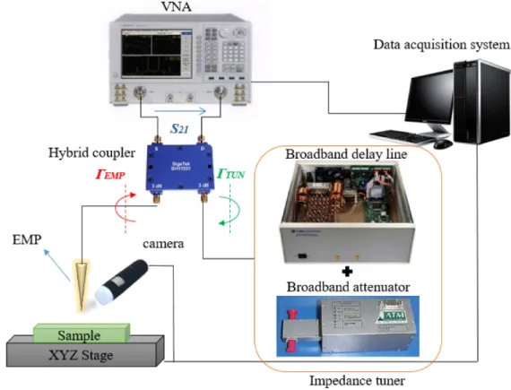
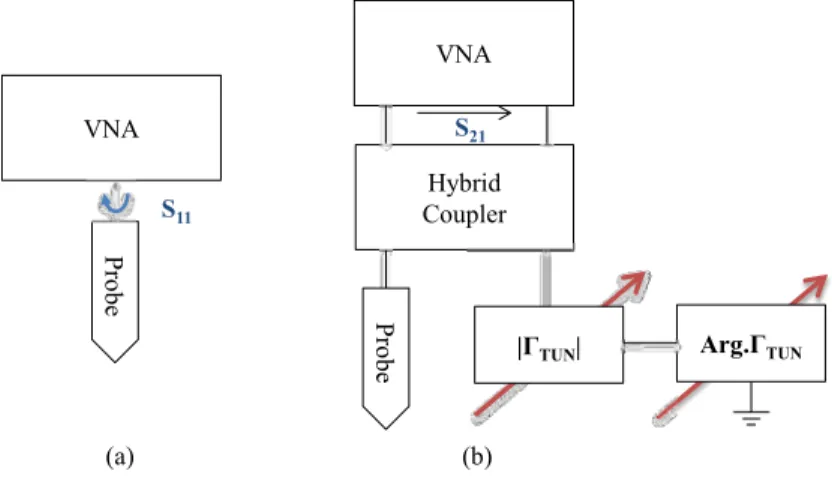
(11) Thèse de Tianjun Lin, Université de Lille, 2018. List of figures ---------------------------------------------------------------------------------------------------------------------. List of figures CHAPTER I FIGURE I-1: SCHEMATIC OF SUBSURFACE DETECTION TOWARDS A DOPED SI SUBSTRATE PARTLY COVERED BY SIO2 FILMS [GRA 15]. .............................................................................................. 10. FIGURE I-2: SUBSURFACE IMAGING RESULTS OF A 100 NM THICK GOLD THIN FILM PATTERN ON A GLASS SUBSTRATE WITH DIFFERENT COVER THICKNESSES RANGING FROM. 0 TO 50 µM [SUN 14].. ....................................................................................................................................................... 11 FIGURE I-3: (A) LUMPED ELEMENT MODEL OF TIP-SAMPLE INTERACTION (B) EQUIVALENT CIRCUIT [GU 16_C]...................................................................................................................................... 13 FIGURE I-4: (A) SCHEMATIC OF A SPLIT RING RESONATOR BASED PROBE (B) AN EXAMPLE OF A FULL WAVE ELECTROMAGNETIC SIMULATION OF THE INTERACTION BETWEEN THE PROBE AND THE SAMPLE [ISA 17]. .......................................................................................................................... 15. FIGURE I-5: SCHEMATIC OF AN INTERFEROMETER-BASED NFMM TO MEASURE THE COMPLEX IMPEDANCE THROUGH A CALIBRATION PROCEDURE [GU 16_C]................................................... 19. FIGURE I-6: SCHEMATIC OF A SIGNAL GENERATION/ACQUISITION SYSTEM: (A) VNA (B) A COMBINATION OF A FREQUENCY SYNTHESIZER AND MULTI-PORT BASED REFLECTOMETER. [HAD. 11].................................................................................................................................................. 22 FIGURE I-7: SCHEMATIC OF TWO TYPES OF XYZ SCANNER: (A) SCANNER INTEGRATED IN AGILENT 5400 AFM/SPM [HAN 08] (B) SCANNER DESIGNED FOR LARGE AREA IMAGING [REN 11]. ....... 24 FIGURE I-8: REFLECTION COEFFICIENT Г AS A FUNCTION OF A PURE RESISTIVE IMPEDANCE (DUT). THE VNA INTRINSIC IMPEDANCE IS 50 Ω [GU 16_C]. .................................................................. 25 FIGURE I-9: SCHEMATIC OF FOUR TYPICAL RESONATOR BASED MATCHING NETWORKS AND AN EXAMPLE OF A MEASURED REFLECTION COEFFICIENT: (A) A SPLIT-RING RESONATOR [REN 11] (B) A RESONANT WAVEGUIDE. [KIM 04] (C) A LOADED APERTURE PROBE [MAL 16] (D) A COAXIAL. RESONATOR [WAN 07] (E) THE MEASURED REFLECTION COEFFICIENT IN TERMS OF MAGNITUDE AT THE RESONANCE FREQUENCY (4.1 GHZ) FOR THE RESONANT WAVEGUIDE [KIM 04].................. 27. vii © 2018 Tous droits réservés.. lilliad.univ-lille.fr.
(12) Thèse de Tianjun Lin, Université de Lille, 2018. List of figures --------------------------------------------------------------------------------------------------------------------FIGURE I-10: SCHEMATIC OF THE INTERFEROMETER BASED MATCHING NETWORK IN TWO MODES; (A) THE REFLECTION MODE WITH AN IMPEDANCE TUNER AND A POWER DIVIDER [BAK 13] (B) THE TRANSMISSION MODE WITH AN IMPEDANCE TUNER AND A HYBRID COUPLER [HAD 12]. ............ 29. FIGURE I-11: THE CANCELLATION PROCEDURE; (A) THE TUNING PROCESS FOR THE Г���. CANCELLATION (B) THE COMBINATION OF THE REFLECTED AND CANCELLATION WAVES [BAK 13],. [GU 16]. ......................................................................................................................................... 30 FIGURE I-12: SCHEMATIC OF DIFFERENT TYPES OF EMP [EI 17]; (A) COAXIAL LINE BASED PROBE (B) APERTURE BASED PROBE (C) STM TIP (D) PARALLEL LINE BASED PROBE (E) AFM PROBE (F) MAGNETIC LOOP PROBE. ............................................................................................................... 32 FIGURE I-13: NORMALIZED ELECTRIC FIELD GENERATED ON A CONDUCTING SUBSTRATE BY EMP WITH DIFFERENT MATERIALS [WU 17]; (A) TITANIUM TIP (B) SILICON TIP. ................................. 32. CHAPTER II FIGURE. II-1:. NEAR-FIELD. MICROWAVE. MICROSCOPE. CONFIGURATION. BASED. ON. INTERFEROMETRY.......................................................................................................................... 46. FIGURE. II-2:. SCHEMATIC. OF. THE. DIFFERENT. CONFIGURATIONS. SIMULATED. BY. KEYSIGHTTM/ADS, (A): WITHOUT INTERFEROMETER, (B): WITH INTERFEROMETER [GU 16_C]. 48 FIGURE II-3: (A) MEASURED (SOLID LINES) AND SIMULATED (DOTTED LINES) MAGNITUDE SPECTRA IN TWO CASES: WITH (IN BLACK) AND WITHOUT (IN RED) INTERFEROMETER; P0 = 0 DBM,. IFBW = 100HZ, EMP APEX SIZE= 66 ΜM. (B) THE CLOSE-UP FIGURE AROUND 2.461 GHZ [GU 16_C]. ............................................................................................................................................ 48 FIGURE II-4: QUALITY FACTORS MEASURED (IN RED) AS A FUNCTION OF THE FREQUENCY CONSIDERING THE ZERO LEVEL AROUND. -75 DB (IN BLUE); (A): RESULTS WHEN USING THE [2-10. GHZ] COUPLER; (B): RESULTS WHEN USING THE [6-18 GHZ] COUPLER; THE WAVE-CANCELLING PROCESS IS DONE CONSIDERING THE PROBE IN AIR [GU 16_C]. .................................................... 50. FIGURE II-5: THE CONTROL INTERFACE INSERTED IN THE DATA ACQUISITION SYSTEM (A) PLATFORM PARAMETERS (B) VNA PARAMETERS. ......................................................................... 52. viii © 2018 Tous droits réservés.. lilliad.univ-lille.fr.
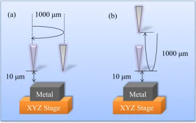
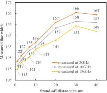
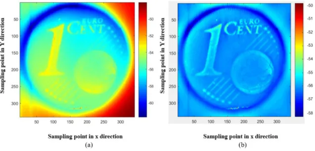
(13) Thèse de Tianjun Lin, Université de Lille, 2018. List of figures --------------------------------------------------------------------------------------------------------------------FIGURE II-6: REPEATABILITY TESTS OF THE MOTORIZED STAGE IN X/Y DIRECTIONS (A) AND IN Z DIRECTION (B), THE DISPLACEMENT IS PERFORMED BY CONSIDERING A STEP OF 1000 ΜM.......... 57. FIGURE II-7: DESCRIPTION OF THE SAMPLE UNDER TEST: (A) GOLD LINES WITH VARIOUS WIDTH FOR THE EVALUATION OF MEASUREMENT PRECISION (B) GOLD LINES WITH FIXED WIDTH BUT DIFFERENT SPACING FOR THE LATERAL RESOLUTION STUDY (C) THE INTERACTION BETWEEN THE PROBE AND SAMPLE. ...................................................................................................................... 62. FIGURE II-8: MEASURED MAGNITUDE OF THE TRANSMISSION COEFFICIENT S21 FOR A GOLD LINE OF. 100 µM WIDTH: (A) RAW DATA, (B) BALANCED DATA, (C) DENOISED DATA, (D) LINEAR. BALANCED AND DENOISED DATA. ................................................................................................. 63. FIGURE II-9: (A) HFSS SIMULATION OF THE ELECTRIC FIELD MAGNITUDE AROUND THE 70 µM PROBE TIP FOR DIFFERENT STAND-OFF DISTANCES H FROM 1 TO 40 µM AT 10 GHZ (B) SENSITIVITY MEASURED WITH THE INFMM FOR DIFFERENT STAND-OFF DISTANCES H FROM 1 TO 40 µM AND THE CORRESPONDING WIDTH MEASURED FOR A 100 µM-WIDTH LINE AT 10 GHZ. .............................. 64. FIGURE II-10: MEASURED GOLD LINE WIDTH AT DIFFERENT STAND-OFF DISTANCE FROM 1 µM TO 40 µM AT 2, 10 AND 18 GHZ WITH A 70 µM EMP. ......................................................................... 65 FIGURE II-11: (A) GOLD LINES WITH VARIOUS WIDTHS (B) MEASURED MAGNITUDE OF THE TRANSMISSION COEFFICIENT S21 OVER A SET OF LINES WITH DIFFERENT WIDTH RANGING FROM 10 ΜM TO. 100 ΜM, PROBE APEX = 30 ΜM, F= 18 GHZ, H=1 ΜM (C) MEASUREMENT CONTRAST. (SENSITIVITY) FOR DIFFERENT GOLD LINES (D) LINE WIDTH MEASURED FOR EACH GOLD LINE COMPARED TO THE ORIGINAL WIDTH. ........................................................................................... 67. FIGURE II-12: (A) SIMULATION OF THE ELECTRIC FIELD MAGNITUDE FOR THE PROBE TIP IN FREE SPACE WITH ANSYSTM/HFSS. THE IMAGE IS TAKEN AT THE CROSS-SECTION ALONG THE PROBE, F =. 18 GHZ. (B) MODEL OF PROBE AND SAMPLE INTERACTION WITH DIFFERENT STAND-OFF DISTANCES. ....................................................................................................................................................... 68 FIGURE II-13: MEASURED LINE WIDTH COMPARED TO THE ORIGINAL WIDTH OF GOLD LINES FROM 20 ΜM TO 40 ΜM WITH AND WITHOUT THE DSP METHOD. ........................................................... 69. ix © 2018 Tous droits réservés.. lilliad.univ-lille.fr.
(14) Thèse de Tianjun Lin, Université de Lille, 2018. List of figures --------------------------------------------------------------------------------------------------------------------FIGURE II-14: MEASURED MAGNITUDE OF THE TRANSMISSION COEFFICIENT S21 BY AN EMP OF 50 µM TIP APEX SIZE (A) RAW DATA, (B) BALANCED DATA, (C) BALANCED AND DENOISED DATA. ZERO LEVEL = -55 DB, F = 18 GHZ, H= 1 µM. ......................................................................................... 71. FIGURE II-15: MEASURED MAGNITUDE AND PHASE SHIFT OF THE TRANSMISSION COEFFICIENT S21, ZERO LEVEL = -55 DB, F = 18 GHZ, H= 1 µM, EMP= 30 µM (A) RAW DATA IN MAGNITUDE (B) BALANCED AND DENOISED DATA IN MAGNITUDE (C) RAW DATA IN PHASE SHIFT (D) BALANCED AND DENOISED DATA IN PHASE SHIFT. .................................................................................................. 72. FIGURE II-16: THE ORIGINAL AND ACQUIRED IMAGE OF AN EURO CENT COIN: (A) ORIGINAL IMAGE (B) THE ACQUIRED IMAGE IN TERMS OF MAGNITUDE OF TRANSMISSION COEFFICIENT S21 (C) SCANNING PATH OF THE ACQUIRED IMAGE. .................................................................................. 74 FIGURE II-17: THE ACQUIRED IMAGE OF THE AN EURO CENT COIN BEFORE/AFTER TREATMENT: (A) THE RAW DATA (B) THE TREATED IMAGE WITH THE PROPOSED ALGORITHM. .............................. 75 FIGURE II-18: THE IMAGE FROM THE FABRICATED ACCELEROMETER ON WAFER: (A) THE IMAGE OF THE ACCELEROMETER (B). THE RAW IMAGE (C) THE TREATED IMAGE WITH THE PROPOSED. ALGORITHM. .................................................................................................................................. 76. FIGURE II-19: MEASURED MAGNITUDE AND PHASE SHIFT OF THE TRANSMISSION COEFFICIENT S21 BY AN EMP WHOSE TIP APEX SIZE IS 30 µM IN CASE OF DIFFERENT THICKNESSES OF COVER LAYER:. (A) MAGNITUDE OF THE TRANSMISSION COEFFICIENT (B) PHASE SHIFT OF THE TRANSMISSION COEFFICIENT. ................................................................................................................................. 78. FIGURE II-20: THE ACQUIRED IMAGE FROM THE FABRICATED ACCELEROMETER ON WAFER: (A) THE RAW IMAGE WITH THE COVER LAYER OF 2 µM (B) THE TREATED IMAGE WITH THE COVER LAYER OF. 2 µM (C) THE RAW IMAGE WITH THE COVER LAYER OF 12 µM (D) THE TREATED IMAGE. WITH THE COVER LAYER OF 12 µM. ............................................................................................... 80. CHAPTER III FIGURE III-1: KEYSIGHT 85070E OPEN-ENDED COAXIAL PROBE [NOT 06]. ............................... 89. x © 2018 Tous droits réservés.. lilliad.univ-lille.fr.
(15) Thèse de Tianjun Lin, Université de Lille, 2018. List of figures --------------------------------------------------------------------------------------------------------------------FIGURE III-2: (A) MICROSTRIP RING RESONATOR [SCH 13] (B) LAMBDA/2 RESONATOR [SCH 14] (C) WHISPERING GALLERY MODE RESONATOR [GUB 15]. ............................................................ 90 FIGURE III-3: (A) SCHEMATIC DIAGRAM OF THE FABRICATED GLUCOSE SENSOR. (B) 3-D VIEW OF THE GLUCOSE SENSOR. (C) SCANNING ELECTRON MICROSCOPE (SEM) PICTURE OF THE CAPACITIVE AIR-BRIDGE STRUCTURE BY. IPD TECHNOLOGY. (D) FORCED ION BEAM (FIB) PICTURE OF THE. CROSS-SECTIONAL VIEW OF THE FABRICATED GLUCOSE SENSOR [DHK 15]. ............................... 91. FIGURE III-4: (A) FABRICATED PROTOTYPES WITH TWO DIFFERENT DIMENSIONS (B) SCATTERING PARAMETERS MEASUREMENTS OF THE FILTER WITH THE VNA (C) PLACEMENT OF THE THUMB ON THE FILTER [BAG 15]. ................................................................................................................... 92. FIGURE III-5: (A) BLOCK DIAGRAM OF NFMM WITH TUNING FORK DISTANCE CONTROL. (B) NFMM MICROWAVE RESONATOR AND PROBE TIP ASSEMBLY [LEE 08]. ..................................... 93 FIGURE III-6: SCHEMATIC OF NFMM, (A): WITHOUT INTERFEROMETER, (B): WITH INTERFEROMETER.................................................................................................................................... 94. FIGURE III-7: HFSS™ SIMULATION RESULTS OF THE REFLECTION COEFFICIENT VERSUS THE EMP POSITION TO THE SOLUTION WITHOUT THE PRESENCE OF INTERFEROMETER-BASED MATCHING NETWORK (FREQUENCY FIXED AT 2 GHZ, CONCENTRATION FROM 0 TO 10 MG/ML): (A) REFLECTION COEFFICIENT MAGNITUDE (B) REFLECTION COEFFICIENT PHASE SHIFT. ....................................... 95. FIGURE III-8: MEASURED TRANSMISSION COEFFICIENTS FOR DIFFERENT IMMERSION DEPTHS OF THE. EMP (FREQUENCY FIXED AT 2 GHZ, CONCENTRATION (0, 10 MG/ML)): (A) MAGNITUDE OF. TRANSMISSION COEFFICIENT (B) PHASE SHIFT OF TRANSMISSION COEFFICIENT........................... 97. FIGURE III-9: THE EXTRACTED COMPLEX PERMITTIVITY OF THE GLUCOSE AQUEOUS SOLUTION IN PHYSIOLOGICAL RANGE VARYING FROM 0 TO 10 MG/ML VERSUS FREQUENCY. (A): THE REAL PART OF THE COMPLEX PERMITTIVITY AND ITS CLOSE UP FIGURE AT 6.5 GHZ. (B): THE IMAGINARY PART OF THE COMPLEX PERMITTIVITY AND ITS CLOSE UP FIGURE AT 6.5 GHZ. ................................... 104. FIGURE III-10: ANALYSIS OF THE PROBE-SOLUTION INTERACTION AT THE CROSS SECTION OF THE EMP (A) FOR A GLUCOSE CONCENTRATION OF 10 MG/ML AT DEPTH OF 300 µM FOR DIFFERENT FREQUENCIES (2 GHZ (B), 10 GHZ (C) AND 18 GHZ (D)). E-FIELD INTENSITY ALONG THE EXTRUDED LINE AT DIFFERENT DISTANCES FROM THE TIP (E). ...................................................................... 105. xi © 2018 Tous droits réservés.. lilliad.univ-lille.fr.
(16) Thèse de Tianjun Lin, Université de Lille, 2018. List of figures --------------------------------------------------------------------------------------------------------------------FIGURE III-11: MEASURED TRANSMISSION COEFFICIENTS (S21) AS A FUNCTION OF GLUCOSE CONCENTRATION: (A) MAGNITUDE AT 2.044 GHZ (B) PHASE SHIFT AT 2.044 GHZ (C) MAGNITUDE AT 18.056 GHZ (D) PHASE SHIFT AT 18.056 GHZ. ....................................................................... 108. FIGURE III-12: MEASURED TRANSMISSION COEFFICIENTS (S21) AS A FUNCTION OF GLUCOSE CONCENTRATION: (A) MAGNITUDE AT 2.044 GHZ (B) PHASE SHIFT AT 2.044 GHZ (C) MAGNITUDE AT 18.056 GHZ (D) PHASE SHIFT AT 18.056 GHZ. DASHED LINE: FITTED POLYNOMIAL LINE AT FIRST ORDER. ......................................................................................................................................... 109. FIGURE III-13: THE COMPLEX PERMITTIVITY OF GLUCOSE-WATER MIXTURE VERSUS FREQUENCY AS A FUNCTION OF CONCENTRATION AND ITS CLOSE UP FIGURES AT 4, 8, 12 AND 16 GHZ: (A) REAL PART OF THE COMPLEX PERMITTIVITY (B) IMAGINARY PART OF THE COMPLEX PERMITTIVITY.. 111. FIGURE III-14: ANALYSIS OF THE PROBE-SOLUTION INTERACTION AT THE CROSS SECTION OF THE EMP TIP FOR NON-CONTACT MODE IN TERMS OF E-FIELD INTENSITY AND DISTRIBUTION (A) THE STAND-OFF DISTANCES INFLUENCE ON THE. E-FIELD INTENSITY FOR A GLUCOSE CONCENTRATION. OF 1.2 MG/ML AT 2 GHZ (B) E-FIELD DISTRIBUTION AT A STANDOFF DISTANCE OF THE PROBE AND SOLUTION (C). 1 µM BETWEEN. THE ZOOM UP FIGURE OF E-FIELD DISTRIBUTION IN AIR (D) THE. ZOOM UP FIGURE OF E-FIELD DISTRIBUTION IN SOLUTION. ......................................................... 114. FIGURE III-15: THE SIMULATED REFLECTION COEFFICIENT OF GLUCOSE-WATER MIXTURE FOR THE CONCENTRATION VARYING FROM BASED MATCHING NETWORK: (A). 0 TO 3 MG/ML AT 2 GHZ WITHOUT THE INTERFEROMETER-. THE MAGNITUDE OF THE REFLECTION COEFFICIENT (B) THE. PHASE SHIFT OF THE REFLECTION COEFFICIENT. DASHED LINE: FITTED POLYNOMIAL LINE AT FIRST ORDER. ......................................................................................................................................... 115. FIGURE III-16: MEASURED TRANSMISSION COEFFICIENTS (S21) AS A FUNCTION OF GLUCOSE CONCENTRATION VARYING FROM 0 TO 3 MG/ML WITH A STEP OF 0.6 MG/ML AT 2.029 GHZ: (A) THE MAGNITUDE OF THE TRANSMISSION COEFFICIENT. (B) COEFFICIENT. (C) MAGNITUDE AT. THE PHASE SHIFT OF THE TRANSMISSION. 2.029 GHZ AS A FUNCTION OF THE GLUCOSE CONCENTRATION. (D) PHASE SHIFT AT 2.029 GHZ AS A FUNCTION OF THE GLUCOSE CONCENTRATION. DASHED LINE: FITTED POLYNOMIAL LINE AT FIRST ORDER. ............................................................................... 117. xii © 2018 Tous droits réservés.. lilliad.univ-lille.fr.
(17) Thèse de Tianjun Lin, Université de Lille, 2018. List of figures --------------------------------------------------------------------------------------------------------------------FIGURE III-17: THE COMPLEX PERMITTIVITY OF GLUCOSE-WATER MIXTURE FOR EACH CONCENTRATION AT 2 GHZ: (A) REAL PART OF THE COMPLEX PERMITTIVITY (B) IMAGINARY PART OF THE COMPLEX PERMITTIVITY.................................................................................................. 119. CHAPTER IV FIGURE IV-1: CIRCUIT SCHEMATIC OF A SIX-PORT JUNCTION [WIL 15]. .................................. 129 FIGURE IV-2: DIFFERENT TYPES OF HYBRID COUPLERS INTEGRATED IN A SIX-PORT JUNCTION. (A) BRANCH LINE COUPLER [QAY 14] (B) SHORT-SLOT COUPLER IN SIW [MAN 15] (C) MULTISECTION COUPLER IN TANDEM STRUCTURE [HON 17] (D) ELLIPTICAL MICROSTRIP-SLOT COUPLER. [WEI 15]. ..................................................................................................................................... 131 FIGURE IV-3: SIX-PORT REFLECTOMETER CONCEPTUAL DIAGRAM WHERE QI (I= 1 TO 5) IS A 3 DB/90° COUPLER.......................................................................................................................... 133. FIGURE IV-4: THE SIX-PORT REFLECTOMETER WITH FIVE BRANCH LINE COUPLERS (A) THE LAYOUT OF BRANCH LINE COUPLER (B) TOP VIEW OF BRANCH LINE COUPLER (C) BOTTOM VIEW OF BRANCH LINE COUPLER USING DEFECT GROUND STRUCTURE TECHNIQUE (DGS) [SHU 14]. ..... 134. FIGURE IV-5: TANDEM STRUCTURE TO REALIZE A 3 DB COUPLER BY CASCADING TWO COUPLERS. ..................................................................................................................................................... 137 FIGURE IV-6: THE COUPLER: A FOUR PORT NETWORK............................................................... 137 FIGURE IV-7: EVEN/ODD MODE EXCITATION OF THE TWO COUPLED LINES. ............................. 140 FIGURE IV-8: SCHEMATIC OF A NINE-SECTION COUPLER. ......................................................... 143 FIGURE IV-9: COUPLING FACTOR R ALONG THE LENGTH OF THE COUPLER. ............................. 145 FIGURE IV-10: THE OFFSET STRIPLINE CONFIGURATION. .......................................................... 146 FIGURE IV-11: TRANSITION ASPECT BETWEEN EACH TWO SUCCESSIVE SECTIONS OF A TANDEM STRUCTURE OF (A) 5 SECTIONS (B) 400 SECTIONS. ...................................................................... 148. xiii © 2018 Tous droits réservés.. lilliad.univ-lille.fr.
(18) Thèse de Tianjun Lin, Université de Lille, 2018. List of figures --------------------------------------------------------------------------------------------------------------------FIGURE IV-12: THE INSERTION LOSS COMPENSATION METHOD IN THE MID CROSS SECTION. (A) ORIGINAL SECTION (B) ROUND CORNER COMPENSATION (C) ROUND COMPENSATION (D) SQUARE COMPENSATION. .......................................................................................................................... 149. FIGURE IV-13: S-PARAMETERS SIMULATION RESULTS WHEN THE ROUND CORNER COMPENSATION METHOD IS APPLIED IN THE MIDDLE CROSS SECTION FOR A 8.34 DB MULTI-SECTION COUPLER (A). S-PARAMETERS MAGNITUDE (B) PHASE SHIFT DIFFERENCE BETWEEN THE OUTPUT PORT 2 AND COUPLING PORT 3. ....................................................................................................................... 150. FIGURE IV-14: S-PARAMETERS SIMULATION RESULTS WHEN THE ROUND COMPENSATION METHOD IS APPLIED IN THE MIDDLE CROSS SECTION FOR A PARAMETERS MAGNITUDE (B). 8.34 DB MULTI-SECTION COUPLER (A) S-. PHASE SHIFT DIFFERENCE BETWEEN THE OUTPUT PORT 2 AND. COUPLING PORT 3. ....................................................................................................................... 151. FIGURE IV-15: S-PARAMETERS SIMULATION RESULTS WHEN THE SQUARE COMPENSATION METHOD IS APPLIED IN THE MIDDLE CROSS SECTION FOR A 8.34 DB MULTI-SECTION COUPLER (A). S-PARAMETERS MAGNITUDE (B) PHASE SHIFT. ........................................................................... 152 FIGURE IV-16: THE AIR GAP PLACED BETWEEN EACH CROSSOVER OF THE PARALLEL-COUPLED LINES AND THE EVEN/ODD MODE PROPAGATION PATH. .............................................................. 154. FIGURE IV-17: S-PARAMETERS SIMULATION RESULTS WHEN THE ISOLATION IMPROVEMENT METHOD IS APPLIED IN THE MIDDLE CROSS SECTION FOR A 8.34 DB MULTI-SECTION COUPLER (A). S-PARAMETERS MAGNITUDE (B) PHASE SHIFT BETWEEN THE OUTPUT PORT 2 AND COUPLING PORT 3. .................................................................................................................................................. 155 FIGURE IV-18: STRUCTURE OF THE 3 DB COUPLER BASED ON THE CASCADE OF TWO 8.34 DB COUPLERS. ................................................................................................................................... 156. FIGURE IV-19: THE 3D DESIGN OF THE PACKAGING TO FIX THE COUPLER CIRCUIT. ................. 156 FIGURE IV-20: PHOTOGRAPH OF THE FABRICATED MULTI-LAYER COUPLER (A) BOTTOM STRIPLINE (B) DUROID 5880 MID LAYER (C) TOP STRIPLINE. ...................................................... 157. FIGURE IV-21: SIMULATED AND MEASURED S-PARAMETERS AS A FUNCTION OF FREQUENCY (A) MAGNITUDE (B) PHASE-SHIFT BETWEEN PORT 2 AND PORT 3. .................................................... 158. xiv © 2018 Tous droits réservés.. lilliad.univ-lille.fr.
(19) Thèse de Tianjun Lin, Université de Lille, 2018. List of figures --------------------------------------------------------------------------------------------------------------------FIGURE IV-22: (A) CONTROLLED IMPEDANCE VIA DESIGN (B) CLOSED PACKAGE OF THE INTERCONNECTION STRUCTURE AND ITS CORRESPONDING REFERENCE LINE (C). EXPLODED VIEW. OF THE TEST. ................................................................................................................................ 160. FIGURE. IV-23:. SIMULATED. AND. MEASURED. TRANSMISSION. COEFFICIENT. OF. THE. INTERCONNECTION AS A FUNCTION OF FREQUENCY COMPARED TO THE REFERENCE LINE TRANSMISSION COEFFICIENT.. (A) TRANSMISSION COEFFICIENT DIFFERENCE (B) PHASE-SHIFT. DIFFERENCE. ................................................................................................................................ 161. FIGURE IV-24: SIX-PORT REFLECTOMETER LAYOUT BASED ON FIVE COUPLERS AND A CONTROLLED IMPEDANCE VIA (THE LAYOUT SIZE IS 13 CM*10 CM). ......................................... 163. FIGURE IV-25: SIX-PORT REFLECTOMETER SIMULATION RESULTS AS A FUNCTION OF FREQUENCY (A) MAGNITUDE OF S-PARAMETERS AT EACH PORT (B) PHASE-SHIFT DIFFERENCE BETWEEN PORT 5 ,PORT 6 AND PORT 3, PORT 4. .................................................................................................... 164 FIGURE IV-26: ONE PORT 3-TERMS ERROR MODEL [RYT 01]. .................................................. 165 FIGURE IV-27: THE FLOWGRAPH SHOWS ALL THE POSSIBLE SIGNAL PATHS. ............................ 166 FIGURE IV-28: THE REFLECTION COEFFICIENT DISTRIBUTION SIMULATION PINK STAR: MEASURED DATA, RED SQUARE: CALIBRATED DATA AND BLUE TRIANGLES: IDEAL DATA. F=2 GHZ. .......... 168. FIGURE IV-29: THE REFLECTION COEFFICIENT DISTRIBUTION SIMULATION PINK STAR: MEASURED DATA, RED SQUARE: CALIBRATED DATA AND BLUE TRIANGLES: IDEAL DATA. F=11 GHZ. ........ 169. FIGURE IV-30: THE REFLECTION COEFFICIENT DISTRIBUTION SIMULATION PINK STAR: MEASURED DATA, RED SQUARE: CALIBRATED DATA AND BLUE TRIANGLES: IDEAL DATA. F=20 GHZ. ........ 169. xv © 2018 Tous droits réservés.. lilliad.univ-lille.fr.
(20) Thèse de Tianjun Lin, Université de Lille, 2018. List of tables ---------------------------------------------------------------------------------------------------------------------. List of tables TABLE I-1: EXAMPLES OF RESONATOR STRUCTURES AS WELL AS THE TRAGET APPLICATIONS. . 28 TABLE II-1: STANDARD DEVIATION OF THE TRANSMISSION COEFFICIENT S21 AS A FUNCTION OF IFBW; ZERO LEVEL = -50 DB, F = 2 GHZ, ACQUISITION TIME = 60 S, NUMBER OF POINT = 60. .... 54 TABLE II-2: STANDARD DEVIATION OF THE TRANSMISSION COEFFICIENT S21 AS A FUNCTION OF NUMBER OF POINT; ZERO LEVEL = -50 DB, F = 2 GHZ, ACQUISITION TIME = 60 S. ........................ 55. TABLE II-3: STANDARD DEVIATION OF THE TRANSMISSION COEFFICIENT S21 AS A FUNCTION OF ACQUISITION TIME; ZERO LEVEL = -50 DB, F = 2 GHZ, NUMBER OF POINT = 600 AND IFBW=100. HZ. ................................................................................................................................................. 55 TABLE II-4: STANDARD DEVIATION OF THE TRANSMISSION COEFFICIENT S21 AS A FUNCTION OF THE ZERO LEVEL; F = 2 GHZ; P0 = 0 DBM, IFBW = 100 HZ, ACQUISITION TIME = 5 MINUTES, NUMBER OF POINT = 600. ............................................................................................................... 56. TABLE II-5: SETTING PARAMETERS FOR THE TEST OF MEASUREMENT REPEATABILITY ACCORDING TO THE SCANNING ERROR. ......................................................................................... 57. TABLE II-6: THE ESTIMATED MEASUREMENT REPEATABILITY IN TERMS OF STANDARD DEVIATION IN X, Y AND Z DIRECTIONS. ........................................................................................ 57. TABLE II-7: SETTING PARAMETERS FOR THE LARGE SURFACE IMAGING OF A ONE CENT EURO COIN. .............................................................................................................................................. 74. TABLE III-1: SETTING PARAMETERS FOR TWO MEASUREMENT MODES IN TERMS OF POWER, IFBW, NUMBER OF FREQUENCY POINTS AND ZERO LEVEL. .......................................................... 98 TABLE III-2: NUMBER OF FREQUENCY POINTS AS A FUNCTION OF IFBW; ZERO LEVEL = -55 DB, F = 2 GHZ, ACQUISITION TIME IS RESPECTIVELY 60 SECOND AND 0.5 SECOND. ............................ 101 TABLE IV-1:THE WORKING FREQUENCY RANGE FOR THE FOUR TYPES OF COUPLER ILLUSTRATED IN FIGURE IV-2. .................................................................................................... 132. TABLE IV-2: THE EVEN MODE IMPEDANCE OF THE 9 SECTIONS TANDEM STRUCTURE WITH THE RIPPLE LEVEL AND THE BANDWIDTH RATIO IN CRISTAL AND YOUNG’S TABLE.......................... 144. TABLE IV-3: THE COMPARISON OF SIMULATION RESULTS FOR DIFFERENT COMPENSATION METHODS. .................................................................................................................................... 153. xvi © 2018 Tous droits réservés.. lilliad.univ-lille.fr.
(21) Thèse de Tianjun Lin, Université de Lille, 2018. List of acronyms and abbreviations ---------------------------------------------------------------------------------------------------------------------. List of acronyms and abbreviations. ADC: ANALOG-TO-DIGITAL CONVERTER ADS: ADVANCED DESIGN SYSTEM AFM: ATOMIC FORCE MICROSCOPE CMOS: COMPLEMENTARY METAL OXIDE SEMICONDUCTOR DNA: DEOXYRIBONUCLEIC ACID DSP: DIGITAL SIGNAL PROCESSOR DUT: DEVICE UNDER TEST EMP: EVANESCENT MICROWAVE PROBE FWHM: FULL WIDTH AT HALF MAXIMUM HFSS: HIGH FREQUENCY STRUCTURE SIMULATOR IBMN: INTERFEROMETER BASED MATCHING NETWORK IC: INTEGRATED CIRCUIT IOT: INTERNET OF THINGS IFBW: INTERMEDIATE FREQUENCY BANDWIDTH INFMM: INTERFEROMETER-BASED NEAR FIELD MICROWAVE MICROSCOPE. LO: LOCAL OSCILLATOR MEMS: MICRO-ELECTRO-MECHANICAL SYSTEM MOS: METAL-OXIDE-SEMICONDUCTOR NFMM: NEAR-FIELD MICROWAVE MICROSCOPE NSOM: NEAR-FIELD SCANNING OPTICAL MICROSCOPE SEM: SCANNING ELECTRON MICROSCOPE SMM: SCANNING MICROWAVE MICROSCOPE SPM: SCANNING PROBE MICROSCOPE. xvii © 2018 Tous droits réservés.. lilliad.univ-lille.fr.
(22) Thèse de Tianjun Lin, Université de Lille, 2018. List of acronyms and abbreviations --------------------------------------------------------------------------------------------------------------------SRR: SPLIT RING RESONATOR STM: SCANNING TUNNELING MICROSCOPE VNA: VECTOR NETWORK ANALYZER. xviii © 2018 Tous droits réservés.. lilliad.univ-lille.fr.
(23) Thèse de Tianjun Lin, Université de Lille, 2018. General introduction ---------------------------------------------------------------------------------------------------------------------. General introduction Microelectronic technology covers almost every aspect of our lives, including consumer electronics, communications, computer-aided technologies and robotics. It also results in the incorporation of electronic devices into equipment specific to each industry. The continuous miniaturization of electronic components leads to more economic energy consumption and better performance but also to an increase of the difficulty to characterize them. The development of well-suited characterization means is therefore needed. Naturally, microscopies are considered as good candidates to respond to this requirement as they are known as the solution of choice to visualize small objects which are hard to be observed from naked eyes. However, the conventional optical microscope fails to observe the microscale and nanoscale devices because of the well-known Abbe diffraction limit [ABB 73]. The scanning probe microscope (SPM) has been therefore developed to bypass this resolution limit and leads to a variety of instruments that give spatial resolutions up to the nanometer. Actually, the scanning tunneling microscope (STM), atomic force microscope (AFM) and scanning electron microscope (SEM) are widely used in industrial and academic laboratories today. In fact, the microscopes mentioned above are characterization tools for materials surface vision. Sub-surface characterization such as subsurface biological anomalies imaging and more generally buried structures characterization cannot be realized. Thus, there is a strong need for new characterization tools to address these ever growing demands of instruments of high spatial resolution and multi-functionalities. The near-field microwave microscope (NFMM) seems to meet all these requirements and is considered at the forefront of science and technology today because it combines the potentials of scanning probe microscope with the power of microwave sensing methods. Benefitting from the material penetration ability brought by the microwaves, nondestructive subsurface evaluation and materials properties (structural, topographic, electronic and magnetic) characterization become possible. The NFMM is based on the interaction between the material properties and the electromagnetic fields emitted by an evanescent microwave probe (EMP). To guaranty the high resolution of the NFMM, both. 1 © 2018 Tous droits réservés.. lilliad.univ-lille.fr.
(24) Thèse de Tianjun Lin, Université de Lille, 2018. General introduction ---------------------------------------------------------------------------------------------------------------------. the probe dimensions and the probe to sample distance have to be much smaller than the free-space wavelength. In this PhD work the main goal is to address applications in surface imaging, subsurface imaging and material properties measurement by means of a homemade NFMM. The manuscript is made of four chapters. The first one is an introduction to the state of art of NFMM, where typical features, advantages and limitations are described. Applications including its ability in surface and subsurface imaging as well as its access to the samples under test physical properties are also illustrated. After that, a classical NFMM set-up is described. All the components including the signal generation system, the scanner and the data acquisition system are depicted. To address the sensitivity limitation, two of the most popular matching networks are described in details. We show that according to various types of probes, different applications at selected operating frequencies can be achieved. In chapter II, a brief description of the NFMM developed at IEMN is firstly given. We show that thanks to an interferometer based matching network, the sensitivity limitation is bypassed and the system is able to operate at any frequency in the working frequency band [2-18 GHz]. The setting parameters are also studied and their influence on the measurement precision is estimated. The homemade interferometer-based NFMM (iNFMM) imaging performance is then evaluated both in surface and subsurface situations. Examples of 1D and 2D images are given to appreciate the strengths and weaknesses of the technique proposed. To improve the image quality, image treatment techniques such as position/signal difference method, adaptive robust statistic method and local regression, likelihood method are applied on raw images collected by the iNFMM. To demonstrate that our homemade iNFMM owns the broad working frequency band feature, high measurement sensitivity and precision, we focus on the dielectric properties measurement of biological aqueous solutions in chapter III. Firstly, an introduction to different characterization methods to measure the glucose concentration of aqueous solutions is given and a well-established model to determine the complex permittivity of 2 © 2018 Tous droits réservés.. lilliad.univ-lille.fr.
(25) Thèse de Tianjun Lin, Université de Lille, 2018. General introduction ---------------------------------------------------------------------------------------------------------------------. different concentrations of glucose aqueous solutions is then selected. After that, two investigation modes are respectively presented: immersion mode and non-contact mode. With a careful study of the setting parameters and taking their measurement error rates into account, it is shown that different concentration ranges of glucose aqueous solutions can be characterized according to the two modes. As a demonstration, the dielectric permittivity of glucose aqueous solutions with concentrations ranging from 0 to 10 mg/ml is studied. After the demonstration of liquids characterization possibility, in chapter IV we focus our attention on the improvement of our iNFMM in terms of integration. The wish to integrate the iNFMM is motivated by its large size and the relatively high cost of the components inside, typically the network analyzer and the impedance tuner. The replacement of the network analyzer is focused here. In fact, the network analyzer has two main functions in the NFMM. The first one is the broadband signal generation with a fixed power level. The second one is the measurement of the signal reflected from the probe with high precision. The signal generation requirement can be easily satisfied. To ensure the signal measurement, a six-port reflectometer can be advantageously envisaged. Compared to the conventional network analyzer, the six-port technique owns a major advantage, which is related to the simplicity of the microwave hardware. In this chapter, a six-port reflectometer configuration is selected to cover the large frequency band targeted [2-20 GHz]. The design procedure, fabrication methods and measurement results are presented and a simple one-port calibration method is also applied on the measurement results to further improve the measurement precision.. 3 © 2018 Tous droits réservés.. lilliad.univ-lille.fr.
(26) Thèse de Tianjun Lin, Université de Lille, 2018. 4 © 2018 Tous droits réservés.. lilliad.univ-lille.fr.
(27) Thèse de Tianjun Lin, Université de Lille, 2018. A brief description of near-field microwave microscopy ---------------------------------------------------------------------------------------------------------------------. Chapter I A brief description of near-field microwave microscopy. 5 © 2018 Tous droits réservés.. lilliad.univ-lille.fr.
(28) Thèse de Tianjun Lin, Université de Lille, 2018. A brief description of near-field microwave microscopy ---------------------------------------------------------------------------------------------------------------------. 6 © 2018 Tous droits réservés.. lilliad.univ-lille.fr.
(29) Thèse de Tianjun Lin, Université de Lille, 2018. A brief description of near-field microwave microscopy ---------------------------------------------------------------------------------------------------------------------. Chapter I : A brief description of near-field microwave microscopy I.1 Introduction Smart devices, connected objects or more generally, the Internet of Things (IOT) has become a sunrise industry to facilitate man’s daily life and improve the living quality. The sensors, actuators and electronic circuits play a very important role in IOT since they are usually embedded in the objects to exchange data. Thanks to the rapid advances in the microelectronic technology, the miniaturization of electronic components leads to a much less power consumption and much higher performance. For instance, the semiconductor manufacturing processes for the complementary metal oxide semiconductor (CMOS) has been improved a lot for the size of gate from 10 µm in the early 1970s to 7 nm in nowadays. Thus, the difficulties to characterize these components increase. Furthermore, the spring up of new materials such as graphene, borophene, germanene and so on, results in an increasing demand of characterization in particular at the nanoscale. Consequently, to fulfil such requirement, the scanning probe microscope (SPM) is proposed in this general context of downscaling. This characterization mean is regarded as an innovative metrology tool which can answer to a large range of challenges at the nanoscale [TSE 05] [EFI 17]. In fact, the continuous development of SPM leads to a variety of instruments that are able to offer nanometer spatial resolutions. Scanning tunneling microscope (STM) is firstly introduced by G. Bining and H. Rohrer in 1981[BIN 82_a] [BIN 82_b]. By means of the tunneling current between the sample and the probe, it becomes the first one to present surface studies with atomic resolution. Nevertheless, the measurement principle limits its use only to conductors. Insulating samples could not be imaged until the advent of the alternating current STM (AC-STM) in 1989 [KOC 89]. At about the same time in the mid1980s, the first generation of atomic force microscope (AFM) came up as a combination of a STM and a stylus profilometer (SP) [BIN 86]. The measurement concept focuses on detecting the interatomic or electromagnetic force between the probe tip and the sample surface. Without the limitation brought by the STM, AFM can be applied not only to conductors but also to insulators and semiconductors. Generally speaking, STM and AFM. 7 © 2018 Tous droits réservés.. lilliad.univ-lille.fr.
(30) Thèse de Tianjun Lin, Université de Lille, 2018. A brief description of near-field microwave microscopy ---------------------------------------------------------------------------------------------------------------------. can both operate in air and liquid conditions and offer a good resolution up to several Å for surface characterization [JUL 93]. Samples physical properties such as conductivity, dielectric constant and dopant intensity are of great interest especially for new materials [GAO 98] [IMT 03] [GU 17]. In addition, sub-surface characterization attracts more and more attention, for example in application fields like defects detection in metals [TAB 99_a], subsurface biological anomalies imaging [WU 04] [GAI 07] [REN 11] and buried structures discovering [HAD 11] [GRA 15] [CHI 12]. Microwave sensing techniques have shown a great potential in these domains thanks to the penetration ability offered which allows a non-destructive subsurface evaluation. In fact, traditional far-field microwave characterization techniques λ. are limited by the low resolution which is in the order of 2 according to Abbe’s criterion. [ABB 73] [ABB 84]. Facing the increasing resolution requirement in the order of submillimetre or even the nanoscale, traditional far-field approach is no longer available. Thus, a method to overcome such resolution restriction is imperative. In 1928, Synge firstly came up with the near-field scanning idea to bypass the Abbe’s criterion [SYN 28]. After that, research works have been established to complete this idea and contribute to set the basis of near-field microwave microscopy (NFMM) [FRA 59] [SOO 62] [BRY 65] [ASH 72] [WAN 90] [TAB 99_a]. Recently, the NFMM idea has been included in the atomic force microscope (AFM) and scanning tunnelling microscope (STM) and the AFM/STM based NFMM were therefore developed at the beginning of 21�ℎ century [ANG 07] [HAN 08]. With the development of the NFMM from theoretical and application perspectives, it can be considered as an innovative and powerful metrology tool for the study of a large range of materials such as bulk samples [IMT 07], buried structures [WU 04] [PLA 11], thin films [TSE 13] [GU 17], electronic materials and devices [IMT 10] [FEN 11], liquids [GU 16_c] [LIN 17] and biological samples [FAR 12]. In this chapter, we firstly present the typical features including the advantages and limitations of the NFMM. Applications including its ability in surface and subsurface imaging as well as its access to samples’ physical properties are also described. After that,. 8 © 2018 Tous droits réservés.. lilliad.univ-lille.fr.
(31) Thèse de Tianjun Lin, Université de Lille, 2018. A brief description of near-field microwave microscopy ---------------------------------------------------------------------------------------------------------------------. a classical NFMM set-up is under investigation. All the components including the signal generation system, the scanner and the data acquisition system are illustrated. To address the sensitivity limitation, two of the most popular matching networks are described in details. We show that according to various types of probes, different applications at selected operating frequencies can be achieved. Finally, we present a homemade interferometer-based NFMM developed in MITEC (Microtechnology and Instrumentation for Thermal and Electromagnetic Characterization) group [Bak 15] [GU 16_c].. I.2 NFMM features and applications I.2.1 Introduction As just mentioned in the introduction of the chapter, different kinds of SPM exist that can offer a spatial resolution up to several Å. However, most of them can only evaluate samples surface profile while the subsurface properties remain a challenge. Adversely, NFMM gives the possibility to characterize quantitatively the subsurface properties of the sample thanks to the penetration ability offered by microwaves. Actually, parameters such as the reflection coefficient, the transmission coefficient or the capacitance can be translated into different materials properties including dielectric constant, conductivity, characteristic impedance and so on, with a proper physical model. In the following sections, we firstly present the subsurface imaging ability brought by the NFMM. After that, materials properties determined from two approaches (semi-empirical method and probesample interaction method) are illustrated. The limitations of NFMM are discussed thereafter and finally a conclusion is given. I.2.2 Subsurface imaging As already said, the NFMM exhibits a pronounced advantage compared to the other types of SPM, thanks to the interrogating waves that have the ability to penetrate through materials and reflect the subsurface properties. Indeed, this phenomena relies on the fact that the embedded structures show different characteristic impedances compared to the cover layer. They interact with the microwave signal and affect its magnitude and phase 9 © 2018 Tous droits réservés.. lilliad.univ-lille.fr.
(32) Thèse de Tianjun Lin, Université de Lille, 2018. A brief description of near-field microwave microscopy ---------------------------------------------------------------------------------------------------------------------. features. This can be observed for example by measuring the reflection coefficient in terms of amplitude and phase shift [TAB 04]. As a result, the NFMM can be used in several applications which have been briefly summarized in the introduction. In order to better understand the subsurface imaging performance brought by the NFMM, a demonstration is given for a doped Si substrate that is partly covered by thin SiO2 films.. Figure I-1: Schematic of subsurface detection towards a doped Si substrate partly covered by SiO2 films [GRA 15].. As illustrated in Figure I-1.a, the NFMM is build up with a vector network analyzer (VNA) and a commercial AFM. The sample under test is a flat doped Si substrate which consists of dopant stripes with different dopant density. SiO2 films with two thicknesses (120 nm and 200 nm) are respectively placed on the dopant stripes to verify their influence on the measurement results (Figure I-1.b and Figure I-1.d). The reflection coefficient in terms of phase shift is therefore obtained in Figure I-1.c (120 nm) and Figure I-1.e (200 nm). One can note that the dopant stripes are clearly detected even with the oxide coverage. Nevertheless, the measured sensitivity between the first and second dopant stripes decreases with the increase of the SiO2 layer thickness. This phenomena gives rise to a discussion: what is the relationship between the measurement sensitivity and the thickness of the cover layer? To answer this question, Sun et al have designed an experiment to evaluate the influence of covers on the subsurface imaging quality [SUN 14].. 10 © 2018 Tous droits réservés.. lilliad.univ-lille.fr.
(33) Thèse de Tianjun Lin, Université de Lille, 2018. A brief description of near-field microwave microscopy ---------------------------------------------------------------------------------------------------------------------. Figure I-2: Subsurface imaging results of a 100 nm thick gold thin film pattern on a glass substrate with different cover thicknesses ranging from 0 to 50 µm [SUN 14].. In this experimentation, the tip apex size is around 50 µm and the tip-sample distance is fixed to 10 µm. The optical image of a gold thin film pattern whose thickness is 100 nm is demonstrated in Figure I-2.a. With the NFMM measurement, the contour views of the pattern are shown in terms of resonant frequency and magnitude of the measured reflection coefficient in Figure I-2.b and Figure I-2.c. A resonant frequency shift of about 0.06 GHz and a magnitude sensitivity of 8 dB are observed. To evaluate the influence brought by the dielectric cover, three configurations are investigated and for each of them the resonant frequency and the reflection coefficient are plotted. The first one does not include a cover (Figure I-2.d and Figure I-2.g) whereas a layer of SU-8 photoresist with a thickness of respectively 25 µm (Figure I-2.e and Figure. 11 © 2018 Tous droits réservés.. lilliad.univ-lille.fr.
(34) Thèse de Tianjun Lin, Université de Lille, 2018. A brief description of near-field microwave microscopy ---------------------------------------------------------------------------------------------------------------------. I-2.h) and 50 µm (Figure I-2.f and Figure I-2.i) is considered for the two other configurations. From the measurement results, one can note that the contrast value (magnitude and resonance phase shift) decreases with the increase of the cover thickness, resulting in a worse lateral resolution and a degraded image quality. If we keep constant the distance between the tip and the cover, the increase of the cover thickness actually leads to a larger tip to sample of interest distance. Thus, the degradation of image quality is supposed to come from two parts: the increase of tip-sample distance and the influence of the dielectric layer. However, if the tip-sample distance is kept constant, the influence can be considered mainly due to the dielectric layer. In this case, the relationship between the measurement sensitivity and the thickness and nature of the cover layer is clearly demonstrated. As a summary, the subsurface imaging is based on the physical properties difference (impedance, dielectric constant, etc.) between the target sample and its coverage layer. One can not only qualitatively observe this variation but also quantitatively obtain the physical properties of the material under the cover layer. In the next section, two important properties which are the dielectric constant and the characteristic impedance are determined by means of two methods. I.2.3 Quantitatively imaging of materials properties In this section, quantitative measurement of materials properties such as dielectric constant and characteristic impedance are demonstrated with NFMM. The imaging technique is mainly based on the knowledge of the electromagnetic interaction between the probe and the sample at microwave frequencies [ANL 07]. The mostly used methods to image the material physical properties are discussed in the following parts. I.2.3.1 Probe-sample interaction method The first technique is called probe-sample interaction method. This method relies on the investigation of the probe-sample interaction and aims to extract the sample physical. 12 © 2018 Tous droits réservés.. lilliad.univ-lille.fr.
(35) Thèse de Tianjun Lin, Université de Lille, 2018. A brief description of near-field microwave microscopy ---------------------------------------------------------------------------------------------------------------------. properties directly from the measured results. In this case, the modelling of the tip-sample interaction becomes very important. The established model together with the knowledge of the tip geometry helps for the sample properties determination [ANL 07]. For instance, this method has been used for complex optical constants characterization with an AFMbased NFMM [HIL 00]. Actually, the modelling of the tip-sample interaction is highly dependent on the probe type. For demonstration, two kinds of probe corresponding to a perfect conducting sphere and a magnetic split ring resonator (SRR) based probe are presented. I.2.3.1.1 The perfect conducting sphere probe Generally, the perfect conducting sphere probe is considered as the most classic one that is used in the NFMM system. As can be seen in Figure I-3.a, it is generally made up with a sharpened metal tip that is mounted on the center conductor of a coaxial connector. The metal tip is a sphere whose radius is the probe apex size D.. Figure I-3: (a) Lumped element model of tip-sample interaction (b) equivalent circuit [GU 16_c].. To describe the interaction between the tip and the sample, a lumped element model is given [GU 16_c]. The impedance �� is regarded as the probe impedance and can be 13 © 2018 Tous droits réservés.. lilliad.univ-lille.fr.
(36) Thèse de Tianjun Lin, Université de Lille, 2018. A brief description of near-field microwave microscopy ---------------------------------------------------------------------------------------------------------------------. calculated by the equivalent circuit illustrated in Figure I-3.b. One can note that three parameters have an influence on the impedance �� , which are the tip-sample capacitance �� , the sample ‘near field’ impedance �� ( �� , �� , �� ) and the tip body to sample capacitance ���� . The sample impedance �� can be further divided into sample resistance �� , inductance �� and capacitance �� [ANL 07] [GU 16_c]. �� −1 = (. 1 + �� )−1 + ������ ����. (� − 1). ZS is related to the energy stored and/or dissipated in the sample. The tip-sample capacitance �� and the tip body to sample capacitance ���� can be calculated with the. distance between the tip and sample (H). To ensure a high sensitivity (Zt ∼ZS), the term 1/��� ZS as well as the term ����� ZS has to be much smaller than or at least on the order. of unity. This condition is satisfied when H is much smaller than the probe apex size D. [ANL 07]. If one consider the near-field impedance is according to a homogeneous bulk sample, the equation I-1 can be further transformed to equation I-2 in the near field region [ANL 07]:. �� =. 1 ���0 �� �. (� − 2). From this equation, one can find it is basically the impedance of a capacitor with a geometrical capacitance �0 �� D filled up with a material of complex relative permittivity εs = ε’ – jε”. This concept can also be applied for different materials such as dielectrics,. semiconductors and normal metals [ANL 07]. Thanks to this model, the relationship between the material dielectric permittivity and the probe characteristic impedance is clear when the tip apex size is known. I.2.3.1.2 The magnetic SRR probe Apart from the classic perfect conducting sphere probe, other types of probes are also able to evaluate the sample properties. Very recently, Dmitry Isakov and his colleagues. 14 © 2018 Tous droits réservés.. lilliad.univ-lille.fr.
(37) Thèse de Tianjun Lin, Université de Lille, 2018. A brief description of near-field microwave microscopy ---------------------------------------------------------------------------------------------------------------------. have proposed a SRR based probe for the relative dielectric permittivity determination [ISA 17]. As can be seen from Figure I-4.a, the SRR is inserted in between two magnetic loops which are connected to the two ports of the VNA. The size of the ring is expressed with an outer radius r, a width w, a height h and a gap width g. In case of free space, the SRR excitation is a time-varying magnetic field which is parallel to the split ring axis. The SRR response comes from the resonant exchange of energy between the electrostatic fields in the capacitive gap and the inductive currents inside the split ring. Thus, the SRR can be considered as a LC circuit with an effective inductance L and a capacitance C with magnetic resonance frequency: �0 = (2�√��)−1. (� − 3). Figure I-4: (a) Schematic of a split ring resonator based probe (b) an example of a full wave electromagnetic simulation of the interaction between the probe and the sample at 15 GHz [ISA 17].. A full wave electromagnetic simulation of the interaction between the probe and sample is illustrated in Figure I-4.b when the SRR is in contact with the sample. The vectors and the color contours indicate the direction and intensity of the induced electric field in the cross section at the resonant frequency. In this case, the capacitance between the SRR and the sample can be assumed to be the sum of the gap capacitance ���� , the ring surface. capacitance ����� and the sample capacitance ������� . 15 © 2018 Tous droits réservés.. lilliad.univ-lille.fr.
Figure
![Figure I-5: A calibration procedure of an interferometer-based NFMM to measure the complex impedance [GU 16_c].](https://thumb-eu.123doks.com/thumbv2/123doknet/3640562.107246/41.918.179.729.323.658/figure-calibration-procedure-interferometer-based-measure-complex-impedance.webp)

![Figure I-13: Normalized electric field generated on a conducting substrate by EMP with different materials [WU 17]; (a) Titanium tip (b) Silicon tip.](https://thumb-eu.123doks.com/thumbv2/123doknet/3640562.107246/54.918.143.780.650.898/normalized-electric-generated-conducting-substrate-different-materials-titanium.webp)
+7


Documents relatifs