HAL Id: tel-01590352
https://hal.archives-ouvertes.fr/tel-01590352
Submitted on 19 Sep 2017
HAL is a multi-disciplinary open access
archive for the deposit and dissemination of sci-entific research documents, whether they are pub-lished or not. The documents may come from teaching and research institutions in France or abroad, or from public or private research centers.
L’archive ouverte pluridisciplinaire HAL, est destinée au dépôt et à la diffusion de documents scientifiques de niveau recherche, publiés ou non, émanant des établissements d’enseignement et de recherche français ou étrangers, des laboratoires publics ou privés.
Public Domain
Fault-mitigation strategies for reliable FPGA
architecture
Chagun Basha Basheer Ahmed
To cite this version:
Chagun Basha Basheer Ahmed. Fault-mitigation strategies for reliable FPGA architecture. Signal and Image processing. Université Rennes 1, 2016. English. �tel-01590352�
ANNÉE 2016
THÈSE / UNIVERSITÉ DE RENNES 1
sous le sceau de l’Université Européenne de Bretagne
pour le grade de
DOCTEUR DE L’UNIVERSITÉ DE RENNES 1
Mention : Traitement du Signal et Télécommunications
École doctorale MATISSE
présentée par
Chagun Basha BASHEER AHMED
préparée à l’unité de recherche IETR – UMR6164 – CNRS
Institut d’Électronique et de Télécommunications de Rennes
Fault-mitigation
strategies for
reliable FPGA
architecture
Thèse soutenue à Nantes le 31 March 2016
devant le jury composé de :
Lionel TORRES
Professeur, Université de Montpellier II / Éxaminateur
Alexandre NKETSA
Professeur, LAAS-Université de Toulouse III/Rapporteur
Loïc LAGADEC
Professeur, Lab-STICC, ENSTA Bretagne/ Rapporteur
Arnaud TISSERAND
Senior Researcher, CNRS-INRIA-IRISA /Éxaminateur
Sébastien PILLEMENT
Professeur, Polytech’Nantes, UBL/ Directeur de thése
Stanislaw J.PIESTRAK
Acknowledgements
I take this opportunity to acknowledge and thank all those people who supported me during my PhD.
First of all, I would like to express my sincere gratitude to my advisor Prof. Sébastien PILLEMENT for his encouragement both at educational and personal levels, for his patience, motivation, moral support, enthusiasm, and immense knowl-edge. His suggestions and remarks have always been productive and constructive that are extremely helpful for my research. I would equally like to thank my co-advisor Prof. Stanislaw J. PIESTRAK for his constructive feedback, comments and suggestions at various stages. I am deeply indebted of both my supervisors for guiding me through all the challenges throughout the span of this thesis work.
I also want to thank all the members of the jury who evaluated this work: Lionel TORRES (Professeur, Université de Montpellier II), Alexandre NKETSA (Professeur, LAAS-Université de Toulouse III), Arnaud TISSERAND (Senior Re-searcher, CNRS-INRIA-IRISA) and Loïc LAGADEC (Professor, Lab-STICC, EN-STA Bretagne).
I would like to express my deep sense of gratitude to the partners of the ARDyT project for all the scientific exchanges and discussions. I am very grateful to the Agence Nationale de la Recherche and the Conseil Régional de Bretagne for the research grant and supporting me to attend and to present papers at conferences which were very important to increase my knowledge and to help the state-of-the-art research. I am equally grateful to the research internship students who contributed to this project: Aurélien Fourny, Amit Karel, Joby Varghese, Meng Zhang, and Shubham Maheshwari.
I would like to take this opportunity to acknowledge the help and support pro-vided by all the administrative staff and research team members at IRISA-ENSSAT Lannion and IETR-Polytech Nantes, for the warm welcome, cultural integration and all the memorable moments. I take this opportunity also to express my sincere thanks to all those who guided, advised and supported me at different times, in technical and non-technical issues. I am thankful to Dr. Daniel Philip, Dr. Pramod Udupa, Dr. Romain Brillu and Dr. Quang Hai Khuat for their consultation and advise on various matters.
Finally, I will always remain in debt to my parents, family and friends for the limitless love, care and support that they have always provided me with. A special thanks to my friend Digvijay Babar for the motivation, encouragement and moral support he provided, which helped me handle many difficult situations during this PhD.
Contents
List of Figures i List of Tables v Résumé xii Abstract xv 1 Introduction 11.1 Field Programmable Gate Arrays (FPGAs) . . . 2
1.1.1 Building Blocks and Architecture Details . . . 4
1.2 Dependable Embedded Systems . . . 11
1.2.1 Threats, Uncertainties and Challenges . . . 14
1.2.1.1 Aging . . . 15
1.2.1.2 Variability . . . 15
1.3 Radiation-induced Faults in Reconfigurable FPGAs . . . 16
1.3.1 Total Ionizing Dose (TID) . . . 16
1.3.2 Single Event Effects (SEE) . . . 17
1.3.2.1 Recoverable and Non-recoverable Effects . . . 18
1.3.3 Multiple Bit Upsets (MBUs) . . . 20
1.4 Contributions . . . 21
1.5 Outline . . . 23
2 Related Work 26 2.1 Physical Radiation-Hardening . . . 27
2.1.1 Silicon on Insulator (SOI) [35] . . . 27
2.1.2 Silicon on Sapphire (SOS) [41] . . . 28
2.1.3 Rad-hard SRAM . . . 30
2.2 Design Based Fault Tolerant Techniques . . . 35
2.2.1 Hardware Redundancy . . . 36
2.2.2 Time Redundancy . . . 39
2.2.3 Configuration Scrubbing and Partial Reconfiguration . . . 41
2.2.4 Error Detection and Correction Codes . . . 42
2.2.5 Hybrid Approaches . . . 46
2.2.6 Selective or Partial Mitigation . . . 49
2.2.7 Fine Granular vs. Coarse Granular Strategies . . . 50
2.3.1 Xilinx Space-grade Virtex-5QV FPGA [91] . . . 52
2.3.2 DeSyRe—On-Demand System Reliability [93] . . . 53
2.4 Summary . . . 54
3 Dynamically Reconfigurable Reliable Architecture—The ARDyT Project 57 3.1 The ARDyT Framework . . . 57
3.1.1 Fault-tolerant Hardware Architecture . . . 58
3.1.2 Supporting Tool-set and Framework . . . 59
3.1.3 Dynamic Reliability Management . . . 62
3.2 ARDyT Overall Architecture . . . 62
3.3 Hardware Architecture and Building Blocks . . . 63
3.3.1 Basic Building Blocks . . . 64
3.3.1.1 Fault-aware Configurable Logic Block (FA-CLB) . . 65
3.3.1.2 Built-in Error Detection and Correction Analysis (EDCA) 67 3.3.1.3 Dedicated Identification of Logic and Routing Bit-stream . . . 69
3.3.2 Grouped Partial Reconfigurable Regions . . . 70
3.3.2.1 Dedicated Functional Units . . . 73
3.3.2.2 Fault Status Register (FSR) . . . 73
3.3.2.3 Cluster Based Health Monitoring . . . 75
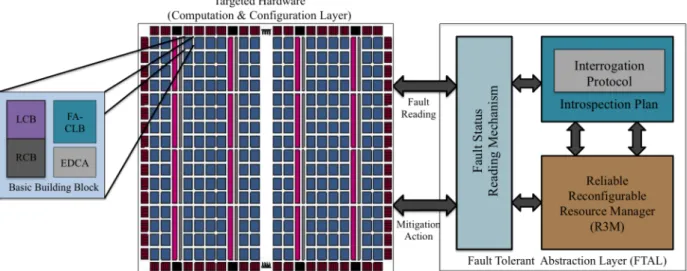
3.4 Dedicated Layer for Reliability Management . . . 77
3.4.1 Fault Tolerant Abstraction Layer (FTAL) as Middle-ware . . . 77
3.4.2 Introspection Plan and Interrogation Protocol . . . 78
3.4.3 Run-time Reconfigurable Resource Manager (R3M) . . . 80
3.5 Summary . . . 82
4 Fault Aware Configurable Logic Block (FA-CLB) 84 4.1 Primitive Elements, Fault Models and Their Consequences . . . 85
4.1.1 Consequences in Combinational Circuit Elements . . . 85
4.1.2 Consequences in Sequential Circuit Elements . . . 85
4.2 Fault-aware Configurable Logic Element (CLE) . . . 86
4.2.1 Fault-aware Combinational Logic Element . . . 87
4.2.2 Fault-aware Sequential Logic Element . . . 89
4.2.3 Hardware Overhead Comparison . . . 89
4.3 Fault-aware CLB for ARDyT FPGA . . . 92
4.3.1 Input Connection Configuration to Adapt DMR . . . 95
4.3.2 Output Connection Configuration to Adapt DMR . . . 96
4.3.3 Architectural Support for Task Re-execution . . . 98
4.4 Fault Mitigation Through the R3M . . . 99
4.4.1 Mitigating Transient Effects . . . 101
4.4.2 Mitigating Upsets in Configuration Bits . . . 101
5 Built-in 3-Dimensional Hamming Multiple-Error Correcting Scheme104 5.1 Proposed 3-Dimensional Hamming (3DH) Multiple-Error Correcting
Code . . . 104
5.1.1 Dealing with Non-correctable Error Pattern . . . 108
5.1.2 Optimizing the Number of Computation . . . 109
5.1.3 Detailed Algorithm of 3DH Code . . . 110
5.2 Functional Implementation of Proposed 3DH Scheme . . . 111
5.2.1 Block Diagram and Description . . . 111
5.2.2 3D Virtualization of 2D Memory . . . 113
5.2.3 Calculation & Storage of Parity Bits . . . 115
5.3 Optimal Size of the 3D Buffer and the Parity Memory Overhead . . . 115
5.3.1 Parity Memory Overhead Comparison . . . 118
5.3.2 Hardware Implementation Details . . . 120
5.4 Reliability Improvement . . . 121
5.5 Fault Mitigation through R3M: Integrating the Proposed Configura-tion ProtecConfigura-tion Scheme in ARDyT FPGA . . . 122
6 Conclusions & Further Works 125 6.1 Main Conclusions & Remarks . . . 125
6.2 Summary of Contributions . . . 126
6.3 Proposed Topics for Future Research . . . 126
6.3.1 3D-Hamming in 3D architectures . . . 126
6.3.2 Distinguishing Logic and Routing Bitstream . . . 127
6.3.3 Fault Mitigation in Routing Resources . . . 127
Bibliography 140
List of Figures
1.1 Generic structure of an FPGA [1]. . . 5
1.2 Basic structure of a sample configurable logic element (CLB) [1]. . . . 5
1.3 Slice architecture of Xilinx 7 Series FPGA [119]. . . 6
1.4 High-level block diagram of the Stratix III ALM [9]. . . 7
1.5 Interconnect points controlled by SRAM cells [98]. . . 8
1.6 Programmable input/output cell [1]. . . 9
1.7 Characterization of dependability and security by their attributes, threats and means [19]. . . 11
1.8 Impact of a high-energy particle: when a high-energy particle (such as a neutron) strikes the silicon substrate of an integrated circuit, it collides with atoms in the substrate [32]. . . 18
1.9 Classes of Single event effects (SEEs) [3]. . . 19
1.10 a) Upset adjacency neighborhood; b) MBU of 3 upset bits [25]. . . 21
2.1 NMOS transistor with bulk CMOS process and with SOI process [38]. 27 2.2 Bulk CMOS and Ultra CMOS (SOS) process [43]. . . 29
2.3 Conventional 6T-SRAM bit-cell [44]. . . 30
2.4 The DICE memory bit-cell [47]. . . 31
2.5 Quad-node 10T or Quatro-10T bit-cell [48]. . . 32
2.6 12T rad-hard SRAM bit-cell [47]. . . 32
2.7 13T rad-hard SRAM bit-cell [50]. . . 33
2.8 Extremely low power SRAM bit-cell (SHIELD) [49]. . . 34
2.9 Dual modular redundancy (DMR) [53]. . . 36
2.10 Triple modular redundancy (TMR) and the majority 2-out-of-3 voter with its truth table [53]. . . 37
2.11 The Xilinx TMR—XTMR scheme [54]. . . 38
2.12 Simple time redundancy scheme [84]. . . 39
2.13 Full time redundancy scheme—An example [84] . . . 40
2.14 Architecture of a traditional scrubbing scheme [57]. . . 41
2.15 EDAC: hardware complexity (logic gate count) vs. BER [66]. . . 44
2.16 2-D HPC: Non-detectable and non-repairable case [66]. . . 46
2.17 ICAP-based internal scrubbing scheme [58]. . . 48
2.18 The hybrid scrubbing system [59]. . . 49
2.19 Implementation of partial TMR: An example [63]. . . 50
2.20 DeSyRe physical partitioning: fault free and fault prone area [93]. . . 53
2.21 DeSyRe logic partitioning: abstraction layers [93]. . . 54
3.2 Modeling code for a 50*50 FA-CLBs FPGA, with 5 inputs and 3
outputs logic elements, and 30-bit interconnection channels. . . 60
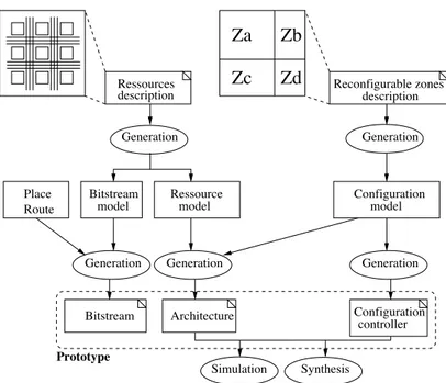
3.3 Global flow supporting generation of a complete environment for re-configurable unit prototyping. . . 61
3.4 Complete vision of the proposed ARDyT FPGA architecture. . . 63
3.5 Physical architecture integration. . . 63
3.6 Hardware architectural hierarchy. . . 64
3.7 Architecture of basic building block. . . 65
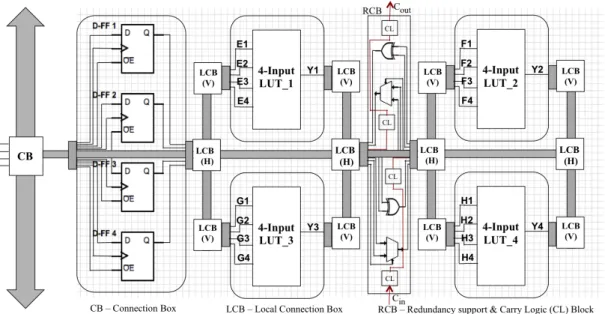
3.8 Fault-aware Configurable logic block (FA-CLB). . . 66
3.9 Interconnections among FA-CLBs. . . 67
3.10 Error detection and correction analysis (EDAC) unit. . . 68
3.11 Fault-aware configurable logic block (FA-CLB) with associated rout-ing elements. . . 69
3.12 Array of logic cells. . . 71
3.13 Connection box (CB) and switch box (SB) structure. . . 71
3.14 Grouped partial reconfigurable regions (GPRR). . . 72
3.15 Dedicated functional units integrated in the FPGA device. . . 73
3.16 Bit definition of the fault status register (FSR). . . 74
3.17 Cluster based health monitoring. . . 76
3.18 Reliability support at different levels. . . 77
3.19 Introspection plan. . . 79
3.20 Super node hash table. . . 79
4.1 Configurable logic element (CLE) architecture of the ARDyT FA-CLB 86 4.2 Transistor-level structure of the 4-input self-checking multiplexer . . . 87
4.3 Proposed structure of the 24 : 1 self-checking multiplexer . . . 88
4.4 Hardware complexity of various schemes of CLE . . . 91
4.5 Fault-aware CLB (FA-CLB) . . . 92
4.6 DMR implementation of the input configuration cell . . . 95
4.7 Simplified connection box architecture . . . 95
4.8 Static DMR configuration . . . 96
4.9 DMR output configuration with output enabled . . . 97
4.10 Dynamic DMR output configuration with enabled input signal . . . . 97
4.11 Freezing the input: Re-execution of One-FA-CLB Task . . . 98
4.12 Freezing the input: Re-execution of Multi-FA-CLB Task . . . 99
4.13 Different stages of fault mitigation in the FA-CLB . . . 100
5.1 General architecture that implements the 3DH error correcting scheme, proposed for SRAM-based FPGAs configuration memory protection. . 104
5.2 Illustration of the 3D Hamming error correcting scheme: (a) Bit po-sitions in terms of 3D co-ordinates (X, Y, and Z) and random errors introduced in data frames; (b) Error correction results after X-axis computation; (c) Error correction results after Y-axis computation; (d) Error correction results after Z-axis computation. . . 105
5.3 Sequence of X-axis Hamming SEC/DED Computation . . . 106
5.4 Sequence of Y-axis Hamming SEC/DED Computation . . . 107
5.6 Dealing with seemingly non-correctable error patterns: (a) Non-correctable 4-tuple error pattern in Z-frame; and (b) The same error pattern
which is correctable in Y-frames . . . 109
5.7 Example Error Pattern- Reducing No. of Computation . . . 109
5.8 Implementation block diagram of the 3D multiple bit error correcting Hamming scheme . . . 112
5.9 3D Virtualization of 2D Memory . . . 113
5.10 3D Virtualization Pattern . . . 114
5.11 2D to 3D virtualization . . . 114
5.12 Configuration organization: (a) 1D word; (b) 2D frame; and (c) 3D buffer . . . 116
5.13 Comparison of the parity memory overhead between 3D encoding using perfect Hamming codes (PH) and standard Hamming codes (SH) applied to n = 2j data bits. . . 117
5.14 Optimal values of the 3D buffer co-ordinates . . . 117
5.15 Comparison of parity memory overhead . . . 119
5.16 (a) Conventional Xilinx CRC & ECC with external golden copy, (b) Proposed built-in scheme without a golden copy . . . 122
List of Tables
2.1 Check bits for SEC and SEC/DED [68] . . . 45
3.1 Fault occurrence status and interpretation in FA-CLBs . . . 74
4.1 Fault models and their consequences in combinational and sequential circuit elements . . . 85
4.2 Transistor count of modules used . . . 90
4.3 Hardware overhead: proposed scheme vs. TMR-protected scheme . . 90
4.4 Hardware overhead: proposed scheme vs. DMR-protected scheme . . 90
4.5 Hardware overhead: proposed scheme vs. scheme in [104] . . . 91
4.6 Resource usage vs. reliability trade-off . . . 94
4.7 DMR output configuration: transistor count comparison . . . 98
5.1 Parity bit estimation (based on equation 5.4) . . . 118
5.2 Parity memory overhead comparison . . . 119
5.3 Hardware resource utilization summary . . . 120
5.4 Comparison: non correctable error patterns of 1D, 2D and 3D ham-ming scheme . . . 121
Résumé
La fiabilité est devenue un facteur essentiel pour la plupart des systèmes de cal-cul intégrés. Malgré les avantages fournis par les circuits reconfigurables (FP-GAs), à savoir une conception à faible coût et un délai rapide de commercialisation, l’importance de la fiabilité risque de limiter leur large utilisation dans les systèmes critiques. Par exemple, dans des missions spatiales non habités, la fiabilité d’un sys-tème de calcul a un impact majeur sur le coût de la mission vu qu’il s’avère difficile de remplacer un système s’il devient défectueux. Aujourd’hui, le besoin de systèmes informatiques fiables s’est développé au-delà des applications militaires et spatiales traditionnelles. Cette liste croissante de domaine inclut les systèmes de communica-tion, les systèmes médicaux et de sauvetages (comme les machine cardio-pulmonaire, les machines de ventilation mécaniques, les pompes de perfusion, les machines de ra-diothérapie, machines de chirurgie robotique, . . . ), les réacteurs nucléaires et autres systèmes de contrôle de centrales électriques, la signalisation dans le transport, et cette liste n’est pas exhaustive.
Les progrès de la technologie CMOS engendrent de nouvelles contraintes en rai-son des limites physiques et économiques de ces process. En particulier, les tailles réduites des transistors impliquent une diminution du rendement et de la précision des System-on- Chip (SoC) en raison de la présence (variabilité) ou l’apparition (vieillissement) de défauts physiques dans le circuit. Ainsi, les défauts induits par les radiations consistuent une grande menace pour les architectures reconfigurables et surtout lorsqu’elles sont utilisées dans des environnements de rayonnement diffi-ciles. La variabilité de fabrication impliquent aussi des complications telles que la fuite sous le seuil, la dissipation de puissance, la sensibilité accrue du circuit au bruit. Tous ces phénomènes induisent, soit des défaillances transitoires (par exemple, er-reurs du logiciel radio-induites par un changement de valeur dans une mémoire), soit permanentes (par exemple, le vieillissement du transistor). Ce besoin de fiabilité ap-porte une révolution dans la pratique de la conception de circuits et requière la prise en compte de la tolérance aux pannes ou l’inclusion de capacités de détection de défauts. C’est un défi important pour les développeurs, quand ils utilisent des FP-GAs du commerce en vue de concevoir des applications critiques. Des stratégies de conception prenant en compte l’atténuation des effets des pannes doivent être mises en œuvre, ainsi qu’un processus de conception adaptÃľ. Cela dépend considérable-ment de plusieurs paramètres incluant la sensibilité de l’application, l’atmosphère de déploiement et le niveau de fiabilité requis.
En termes de la mise en œuvre de systèmes complexes, les circuits FPGA re-configurables font désormais partis de l’ordinaire grâce à leur flexibilité, leurs per-formances et leur nombre élevé de ressources intégrées. Les architectures
recon-figurables présentent un compromis subtil entre complexité et la flexibilité néces-saire. Les champs récents d’applications des FPGA correspondent à des environ-nements difficiles (rayonnement cosmique, ionisants, bruit électromagnétique) et avec de hautes exigences de tolérance aux fautes. Les FPGAs récents ne sont pas adaptés à ce type d’environnement à l’exception de circuits bien spécifiques ayant été durci mais avec un prix de revient très élevé, ce qui les rend moins intéressant d’un point de vue économique. Par conséquent, de nouvelles alternatives doivent être envisagées.
La plupart des FPGA du commerce (COTS pour Components Of the Shelf) ne parviennent pas à répondre aux exigences des systèmes critiques (sauf quelques dis-positifs tels que les Virtex-5QV de Xilinx et le Microsemi RTG4). Ceci est dû à leur grande sensibilité aux événements qui créent des fautes et des incertitudes notam-ment dans la mémoire de configuration basée sur une technologie SRAM très sensible aux radiations. Beaucoup de développeurs ont compris que les systèmes essentiels à la mission doivent être conçus pour un fonctionnement fiable dans des conditions environnementales extrêmes, mais constatent que la plupart des technologies FPGA ne peuvent pas répondre à ces besoins. Pour supporter ces environnements agressifs, les phénomènes transitoires et les effets d’un seul événement, les systèmes critiques nécessitent des composants fiables.
Dans la majorité des cas, pour atteindre le niveau désiré de fiabilité dans les ap-plications basées sur des circuits reconfigurables, deux stratégies traditionnelles sont suivies, i) faire une architecture entièrement durcie au rayonnement par le processus de fabrication lui-même et ii) par l’application de diverses stratégies de tolérance aux fautes intégrés aux architectures COTS au stade de la conception de l’application. Les deux solutions de durcissement et de conception sur lesquels les solutions sont basées ont leurs propres avantages et inconvénients. Une solution alternative plus intéressante, où les avantages des différentes approches pourraient être utilisés, en termes de surcoût matériel, consommation d’énergie, l’amélioration de la fiabilité et la souplesse de conception, etc. peut être envisagé. Nous proposons donc le développement de nouvelles architectures fiables, où divers mécanismes de fiabilité peuvent être intégrés à différents niveaux de l’architecture, y compris les processus de fabrication, l’architecture matérielle, le plan de configuration, la conception de l’application afin de soutenir le niveau de fiabilitÃľ requis mais sans payer le prix du durcissement technologique du circuit.
Contributions
Ce travail de thèse a pour objectif de remédier à ces inconvénients et à ces défis en proposant des stratégies de gestion de fautes appropriées, et adaptables. La recherche présentée dans cette thèse fait partie intégrante du projet de recherche ANR ARDyT ("Architecture Reconfigurable Dynamiquement Tolérante aux fautes"). Le but de ce travail est de développer des stratégies adhoc de tolÃľrances aux fautes pour protéger les diverses ressources constitutives d’une architecture FPGA. Le tra-vail dans cette thèse est principalement axé sur l’architecture matérielle et le pro-cessus de gestion des fautes. Les contributions de ce travail de recherche sont les suivantes :
• les différents modèles de fautes qui se produisent dans les circuits reconfig-urables ont été étudiés. Ainsi différents modèles d’erreurs associés aux dif-férents éléments constitutifs de l’architecture FPGA ont été étudiés montrant la nécessité d’adapter les stratégies aux différents scénarii. Les différents sys-tèmes de détection et de correction de fautes de l’état de l’art sont ensuite analysés et leurs avantages et inconvénients sont comparés les uns aux autres, en fonction de différents paramètres important dans le cadre des architectures reconfigurables. Les paramètres étudiés comprennent le surcoût matériel, le coût de mise en œuvre, la complexité de la conception, les contraintes de temps, et l’adaptabilité. Puis, il a été répondu à la question : "comment faire une architecture FPGA fiable en faisant une classification générale significative des différentes approches ?". Les différentes approches ont été classées en trois grandes classes : i) conception de l’architecture durcie au rayonnement par fabrication, ii) réalisation de la fiabilité en mettant en œuvre au niveau archi-tecture des techniques de tolérances aux fautes iii) intégration de mécanisme de fiabilité au niveau applicatif (i.e. sans modifier l’architecture).
• Par la suite, les blocs de base de construction de l’architecture matérielle ARDyT sont définis. Des ressources spÃľcifiques pour la détection des fautes, le diagnostic et la tolérance sont ajoutés aux composants logiques comme des fonctionnalités intégrées. Les ressources logiques sont définies afin de per-mettre des compromis entre densité d’intÃľgration et fiabilité fonctionnelle. L’architecture est adaptable est permet de supporter les diffétes stratégies de tolérance aux fautes proposées. Nous avons définie et spécifié une couche d’abstraction fonctionnelle de la tolérance aux fautes (FTAL - Fault-Tolerant Abstraction Layer) et l’algorithme de gestion et de tolÃľrance aux fautes pour les différents modes adaptés sont intégrés dans le R3M (Run-time Reconfig-urable Resource Manager), gestionnaire de la fiabilité centralisé de notre ar-chitecture. La granularité de la détection des fautes et leur notification est déterminée sur la base de régions reconfigurables partielles groupées (GPRR). La première étape d’amélioration de la fiabilité concerne la détection de la dite faute. La remontée d’informations pertinentes sur l’événement survenu (changement de valeur / faute / erreur) contribue à une meilleure formulation de la stratÃľgie de prise en compte de cet événement. Pour faciliter la lecture de l’état de la faute (de sa notification) et de fournir le lien vers le R3M, un registre d’état de faute (FSR - Fault Status Register) est défini dans chaque GPRR. Un protocole d’interrogation est alors employé afin de remonter vers le R3M le type de faute identifié et d’adapter la technique de gestion de la faute appropriée. Ici, le terme "lecture de faute" se réfère à l’identification de la faute qui a eu lieu dans les modules matériel "fault-aware". La nature de la "lecture de faute" dans le cadre du projet ARDyT dépend de différents facteurs tels que la granularité de l’identification de la faute, le mode de représentation de la faute, le temps et le coût matériel requis par la technique de gestion de la faute. Selon les spécifications architecturales proposées et la définition de la FTAL, le protocole d’interrogation a l’accès aux FSR de chaque GPRR. • Dans les FPGA à base de mémoire SRAM, Les cellules mémoires
sauvegar-dent principalement des bits de configuration, occupant plus de 98% de toute la mémoire de la plupart des composants du commerce. Ces bits de configura-tion SRAM sont sujets à des radiaconfigura-tions induites de type SEU (provoquant des changements de valeur d’un seul bit SBU ou de plusieurs bits MBU). En raison du fait que la fonctionnalité d’un FPGA à base de SRAM est déterminée par le contenu de ces cellules de mémoire de configuration, chaque modification des bits de configuration par un SEU modifie la fonctionnalité du dispositif programmé dans le FPGA. Dans ce travail, un nouveau schéma de protection, construit sur un codage de Hamming 3D (3DH - 3-Dimensional Hamming) per-met de gérer les erreurs binaires multiples (SBU et MBU) causées par le rayon-nement dans la mémoire de configuration. L’idée est de réaliser la protection de la mémoire de configuration (bitstream) par le système 3D-Hamming pro-posé s’exécutant en arrière-plan pendant l’exécution de l’application, comme cela se fait dans les dispositifs Xilinx Virtex. Dans le système de protection de proposé, la détection et la correction des erreurs se produisent comme un processus cyclique continu, en raison du fait que les codes de Hamming ne dé-tectent pas seulement l’erreur, mais localise sa position dans le mot binaire et permettent une correction si une seule erreur est présente dans le mot en cours de traitement. La principale différence et avantage du système proposé par rapport à la méthode classique utilisée dans les architectures Xilinx, est que la technique ne nécessite pas l’utilisation d’une copie externe des bits de config-uration. Le schéma 3DH proposé est implémenté grâce aux ressources d’accès internes au bitstream de configuration (ICAP - Internal Configuration Access Port) et entièrement gérés par le gestionnaire centralisé de la fiabilité (R3M) dans la FTAL. Il supporte une reconfiguration rapide des zones de mémoire concernées par les erreurs multiples, parce que la correction peut être faite en utilisant le bus interne seul, contrairement aux méthodes les plus connues qui reposent sur la sauvegarde de la configuration en externe et qui nécessitent le transfert des données via les lignes d’E/S.
• La tolérance aux fautes présentée ci-dessus gère seulement les changements de valeurs qui affectent le flux binaire de configuration, malheureusement, il y a d’autres sources de défauts qui peuvent affecter directement les ressources matérielles du FPGA. Leurs natures et leurs conséquences sont différentes de celles qui se produisent dans bitstream et leurs effets ne peuvent pas être corrigés en effectuant une re-configuration. De fait, pour protéger ces ressources logiques une nouvelle architecture, le FA-CLB (Fault-Aware Con-figurable Logic Block), est proposée qui est capable de détecter en ligne (en fonctionnement normal) des défauts a un niveau fin de granularité (à savoir le niveau LUT pour Look-Up Table). L’approche proposée repose sur l’identifica-tion des défauts des circuits combinatoires et séquentiels séparément, ce qui aide à trouver un défaut et à adapter sa gestion en fonction de sa nature. En ce qui concerne les multiplexeurs des blocs logiques combinatoires, ils ne peuvent pas être directement affectés par un SEU radio-induit qui pourrait provoquer des SBU et / ou MBU, car ils ne contiennent pas d’éléments de stockage. Les modèles de fautes affectant les circuits combinatoires et les circuits séquentiels sont différents. Par conséquent, différents schémas de détection de fautes sont
proposés pour les éléments combinatoires et séquentiels. L’architecture globale du FA-CLB résultante proposée est différente de la structure CLB classique utilisée dans les FPGA commerciaux. Elle intègre notamment les ressources de détection des fautes mais aussi aide la stratégie de gestion de ces fautes grâce notamment á sa structure permettant la redondance temporelle d’un calcul.
Conclusions :
1. La constante mise à l’échelle de la technologie et les changements de carac-téristiques des environnements de fonctionnement des applications augmentent les erreurs dans la mémoire de configuration des architectures reconfigurables. Les niveaux élevés de rayonnement implique l’apparition de fautes multiples de type MBU (multi-bit upset). Ces niveaux de rayonnement déclenchant des changements de valeurs ne se limite plus seulement à l’espace et aux hautes altitudes. Même au niveau du sol, le rayonnement naturel et artificiel des par-ticules est maintenant observé. De même les architectures sont elles même plus sensible à ces rayonnements du fait de la diminution des tailles de transistors. Par conséquent, les systèmes électroniques de haute fiabilité prennent de plus en plus d’importance dans les applications au niveau du sol également. 2. Comme le marché est en pleine expansion au-delà des applications spatiales,
acceptant des coût élevé, il y a un besoin de développer une architecture fi-able et flexible, ciblant une fiabilité à faible coût et permettant l’intégration d’applications critiques. Les architectures durcies par un processus de fabrica-tion spécifique représentent un coût élevé qui ne peut pas être abordable dans de nombreuses applications grand public (comme l’automobile par exemple). Les approches de la tolérance aux fautes utilisées dans les FPGA COTS à base de redondance impliquent une complexité de conception supplémentaire et réduisent la flexibilité de conception. Par conséquent, le développement de nouveaux modèles d’architectures intégrant des mécanismes de support de la fiabilité adaptées à différents niveaux (architecture, configuration, application et logiciel) est nécessaire pour avoir des implémentations d’applications moins complexes, flexibles et à des coûts acceptables pour le grand public.
3. Les effets du rayonnement cosmique ont différents modèles de défaut sur les différents éléments des circuits reconfigurables qui entraînent des conséquences diverses selon leur nature. De ce fait, les techniques de détection et de prise en compte des défauts doivent être adaptées.
4. Le développement de modules logiques adaptables, où les circuits logiques sont personnalisés pour soutenir les stratégies de détection et de correction des fautes est nécessaire et a été réalisé dans ce travail pour le développement d’une architecture reconfigurable. Cela permet de réduire considérablement la complexité de la phase de développement de l’application et le temps d’accès au marché, vu que le concepteur n’a pas à se concentrer sur "l’allocation et l’utilisation des ressources" pour les aspects de fiabilité (comme dans le cas de la conception d’applications fiables sur des architectures non fiables).
5. Un compromis peut être obtenue entre "le niveau de fiabilité" et "le surcoût matériel, la latence, l’efficacité énergétique". Il peut être représenté collective-ment par le facteur d’évaluation de la fiabilité et de l’efficacité. Il est basé sur divers aspects, y compris la sensibilité des différentes tâches ; le suivi et la non surveillance dynamique de zones du circuit ; et la granularité de la détection et de la correction des fautes. Dans le cadre du projet ARDyT un mécanisme de compromis entre densité d’intégration et fiabilité est introduit permettant tout un panel de niveau de fiabilité vs éfficacité (au sens large).
Abstract in French
Les circuits reconfigurables (Field Programmable Gate Arrays - FPGAs) sont large-ment utilisés dans divers domaines d’application en raison de leur flexibilité, de leur haute densité d’intégration, de leur niveau de performance et du faible coût de développement associé. Toutefois, leur grande sensibilité aux défauts dus aux rayonnements électromagnétiques tels que les "Single Event Effets" (SEE), est un défi qui doit être abordé pendant la conception du système. Ces SEE sont une préoccupation majeure dans la sécurité et pour les systèmes critiques tels que les systèmes automobile et avionique. En général, la plupart des FPGA d’aujourd’hui ne sont pas conçus pour fonctionner dans ces environnements difficiles, sauf pour les circuits spécifiques qui ont été durcis par construction au niveau du processus de fabrication. Ces circuits ont un surcoût très élevé et des performances moindres, ce qui les rend moins intéressants que leurs équivalents non protégés.
Le projet ARDyT vise à développer une architecture FPGA fiable à faible coût avec une suite d’outils de conception, offrant un environnement complet pour la conception d’un système tolérant aux fautes. Ce travail de thèse présente une con-tribution à l’architecture du FPGA ARDyT, qui intègre des stratégies de prises en charge des fautes adaptées aux différents éléments de l’architecture. L’un des principaux objectifs du projet ARDyT est de gérer les changements de valeurs mul-tiples (multi bit upsets (MBUs)) dans le flux binaire de configuration du FPGA. Ces stratégies de tolérance aux fautes pour protéger les ressources logiques et le flux binaire de configuration sont discutées en détail. Une architecture spécifique du bloc logique élémentaire configurable est proposée afin de simplifier la stratégie de prise en compte des fautes dans les ressources logiques. Un nouveau système de correction d’erreur intégrée (3-Dimensional Hamming - 3DH) est proposé pour gérer les MBU dans le flux binaire de configuration. L’ensemble de cette stratégie de gestion de fautes est implémenté dans l’architecture au travers d’un manager de la fiabilité centralisée nommée R3M (Run-time Reconfigurable Resource Manager).
Abstract
Reconfigurable Field Programmable Gate Arrays (FPGAs) are extensively employed in various application domains due to their flexibility, high–density functionality, high performance and low–cost development compared to ASICs (Application Spe-cific Integrated Circuits). However, the challenge that must be tackled during sys-tem design is their high susceptibility to the radiation induced faults such as Single Event Effects (SEEs). These radiation induced faults are a major concern in safety and mission critical systems such as automotive and avionics systems. In general, most of today’s commercial off-the shelf (COTS) FPGAs are not designed to work under these harsh environments, except for specific circuits that have been radiation– hardened at the fabrication process level, but at a very high cost overhead, which makes them less interesting from an economic and performance point of view.
Design based techniques and architectural customization are the other ways to achieve desired level of reliability in a system design. This thesis work is a part of a multi-partner project–ARDyT, which aims to develop a low–cost reliable FPGA architecture with supporting EDA tool-suite that offers a complete environment for a fault tolerant system design. The ARDyT FPGA architecture plans to incorporate appropriate fault mitigation strategies at different level of the architecture. The work carried-out in this thesis focus mainly on developing reliability strategies at hardware and configuration level. A fault-aware customized configurable logic block architecture is proposed to support fault mitigation process in configurable logic resources. One of the main objectives of ARDyT project is to handle multi-bit upsets (MBUs) in the configuration bitstream. A new built–in 3–Dimensional Hamming (3DH) error correcting scheme is proposed to handle MBUs in the configuration bitstream. Proposed schemes are made adaptable in such a way that they are integrated in the ARDyT architectural framework to support the global (centralized) reliability management strategy.
Chapter 1
Introduction
Prompted by the development of new types of sophisticated field-programmable devices (FPDs), the process of designing digital hardware has changed dramatically over the past few years. The most compelling advantages of FPDs are instant manufacturing turnaround, low start-up costs, low financial risk and ease of design changes. Field Programmable Device is a general term that refers to any type of integrated circuit used for implementing digital hardware, where the chip can be configured by the end-user to realize different designs. The FPD market has grown over the past decade to the point, where there is now a wide assortment of devices to choose from. To choose a product, designers face the daunting task of researching the best uses of various chips and learning the intricacies of vendor-specific CAD software. Adding to the difficulty is the complexity of the more sophisticated devices. User-programmable switches are the key to user customization of FPDs.
A programmable logic device (PLDs) refers to any type of integrated circuit used to build user-configurable digital circuits. A PLD has an undefined function at the time of manufacturing. Since these logic devices can be programmed in the field, they are also called field programmable logic devices (FPLDs). PLDs come in two forms, complex programmable logic devices (CPLDs) and field programmable gate arrays (FPGAs), both having their advantages and disadvantages with respect to the specific application or design they are to be used in. The primary differences between CPLDs and FPGAs are architectural. A CPLD has a somewhat restrictive structure consisting of one or more programmable sum-of-products logic arrays feed-ing a relatively small number of clocked registers, which results in less flexibility, with the advantage of more predictable timing delays and a higher logic-to-interconnect ratio. The FPGA architectures, on the other hand, are dominated by interconnec-tions, which makes them far more flexible (in terms of the range of designs that are practical for implementation within them) but also far more complex to design for. In practice, the distinction between FPGAs and CPLDs is often one of size, as FPGAs are usually much larger in terms of resources than CPLDs. Typically, only FPGAs contain more complex embedded functions such as adders, multipliers, and memory. Being the only type of FPD that supports very high logic capacity, FPGAs have been responsible for a major shift in the way digital circuits are designed [1]. FPGAs provide many advantages such as:
are completely configurable. Updates and feature enhancement can be carried out in the field, even after deployment.
• Extremely short time to market: Through the use of FPGAs, the devel-opment of hardware prototypes is significantly accelerated since a large part of the hardware development process is shifted to developing the core design, which can be done in parallel. Additionally, because of the early availability of hardware prototypes, time-consuming activities like the start-up and debug-ging of hardware are brought forward concurrently to the overall development. • Fast and efficient systems: Available standard components address a broad user group and, consequently, often constitute a compromise between perfor-mance and compatibility. With FPGAs, systems can be developed that are exactly customized for the designated task, which henceforth can be highly efficient.
• Performance gain for software applications: Complex tasks are often handled through software implementations in combination with high-performance processors. In this case, FPGAs provide a competitive alternative, which by means of parallelization and customization for the specific task even establishes an additional performance gain.
• Massively parallel data processing: The amount of data in contemporary systems is ever increasing, which leads to the problem that systems working sequential are no longer able to process the data on time. Especially by means of parallelization, FPGAs provide a solution to this problem which, in addition, scales excellently.
• Real time applications: FPGAs are perfectly suitable for applications in time-critical systems. In contrast to software based solutions with real time op-erating systems, FPGAs provide real deterministic behavior. By means of the featured flexibility even complex computations can be executed in extremely short periods.
In modern circuits, design flexibility is mandatory, as it enables fast evaluation of design changes during the lifetime of applications, enhancement of functionality, and so on. In counterpart, most of current applications are requiring more and more high computation capability to offer advanced services. In terms of complex sys-tems implementation, programmable FPGA circuits are now part of the mainstream implementation solutions: thanks to their flexibility, good performances and high number of integrated resources. Besides, FPGAs are entering new fields of applica-tions such as aeronautics, military, automotive or confined control, thanks to their ability to be remotely updated [2].
1.1
Field Programmable Gate Arrays (FPGAs)
FPGAs contain programmable logic blocks that can be wired in different configura-tions. These blocks create a physical array of logic gates that can be used to perform
different operations. Because the gates are customizable, FPGAs can be optimized for any computing task.
Based on implementation technology, FPGA architecture could be broadly clas-sified into three types: i) Antifuse-based, ii) Flash-based and iii) Static Random Access Memory (SRAM)-based.
Antifuse-based FPGAs
They can be programmed only once. The antifuse is a device that doesn’t conduct current initially, but can be "burned" to conduct current (the antifuse behavior is thus opposite to that of the fuse, hence the name). The antifuse-based FPGAs can’t be then reprogrammed anymore, since there is no way to return a burned antifuse into the initial state. Antifuse-based device families include Axcelerator producedR
by Microsemi [6]. Flash-based FPGAs
First of all, these type of FPGAs shouldn’t be confused with SRAM-based FPGAs, as the internal flash memory of the latter ones uses flash only during startup to load data to the SRAM configuration cells. On the contrary, a true flash-based FPGA uses flash as a primary resource for configuration storage and doesn’t require SRAM. The main advantages of this technology are low power consumption and better tolerant to radiation effects. Flash-based FPGA families such as Igloo [7] and ProASIC3 [8] are manufactured by Microsemi.
SRAM-based FPGAs
SRAM-based FPGAs store logic cells configuration data in the static memory (or-ganized as an array of latches). Since SRAM is volatile and can’t keep data without power source, such FPGAs must be programmed (configured) upon start. There are two basic modes of programming:
• Master mode, when an FPGA reads configuration data from an external source, such as an external flash memory chip.
• Slave mode, when an FPGA is configured by an external master device, such as a processor. This can be usually done via a dedicated configuration interface or via a boundary-scan (JTAG) interface.
SRAM-based configuration memory is more commonly used in today’s advanced reconfigurable architectures. In this case, each configuration bit is presented as a field-effect transistor (FET) that is controlled by an SRAM cell. Xilinx and Altera are two major SRAM-based FPGA manufacturers. The V irtex family FPGAs from Xilinx (V5 [13], V6 [14], and V7 [15]) and Stratix family FPGAs from Altera [16] are examples of SRAM-based FPGAs. One disadvantage of this technology is that an SRAM-based FPGA always has to be re-programmed at the power up of the circuit board. There are a variety of techniques by which this programming may be achieved; a very common alternative is to use an external serial flash memory chip,
and for the FPGA to instigate the configuration process by reading the contents of this flash memory and using it to program its SRAM based configuration cells. An important advantage of SRAM-based FPGAs is that they can be manufactured using a standard CMOS process, hence they become available right at the forefront of each new technology, thereby offering the highest performance and lowest power consumption. By comparison, flash-based and antifuse-based FPGAs require extra processing steps during the manufacturing process, which means they typically lag the state-of-the-art by one or two technology feature sizes.
Antifuse-based FPGAs have to be configured using a special programming device before being attached to the circuit board. Flash-based FPGAs can be configured off-board—using a special programmer, or on-board—using additional circuitry on the circuit board. And, as previously noted, SRAM-based FPGAs always have to be re-programmed when the board is powered up.
Some devices [10–12] have both a flash transistor and an SRAM cell associated with each configuration bit [2]. Hence, on power-up, the contents of all of the flash transistors are copied (in a massively parallel fashion) into their corresponding SRAM cells. In addition to providing the advantages of non-volatility and instant-on, this also means that the flash portion of the FPGA can subsequently be re-programmed "on-the-fly" whilst the rest of the FPGA is performing its allotted tasks.
1.1.1
Building Blocks and Architecture Details
Figure 2.1 shows a sample FPGA architecture. In general, FPGAs comprise an array of uncommitted circuit elements, called programmable logic blocks, programmable routing (interconnects) and programmable I/O blocks. A programmable logic block provides the basic computation and storage elements used in digital systems. The basic logic element contains some form of programmable combinational logic, a flip-flop and some fast arithmetic carry logic. The programmable routing provides connections among logic blocks and I/O blocks to complete a user defined design. It consists of multiplexers, pass transistors and tri-state buffers, which form the desired connections. Generally, pass transistors and multiplexers are used within a logic cluster to connect logic elements together, while all three types of connection elements are used for more global routing structures.
Configurable Logic Blocks (CLBs)
A configurable logic block (CLB) is the basic building block of an FPGA, capable of realizing arbitrary logic functions. It contains a small memory for creating ar-bitrary combinatorial logic functions, also known as look-up table (LUT). It also contains flip-flops as clocked storage elements as well as multiplexers used to route the logic within the block and to and from external resources. The multiplexers also allow polarity selection as well as reset and clear input selection. Figure 2.5 shows a simplified sample structure of a CLB, which comprises only a 4-input LUT, a multiplexer and a register. The multiplexer requires an associated configuration cell to specify input to be selected. The register requires associated cells which al-low to specify whether it acts as an edge-triggered flip-flop or a level-sensitive latch,
Figure 1.1 – Generic structure of an FPGA [1].
whether it is positive- or negative-edge triggered (in the case of the flip-flop option), whether an enable signal is active-low or active-high (if the register is instructed to act as a latch), and whether it is initialized with a logic 0 or a logic 1. The 4-input LUT is itself based on 16 configuration cells. In reconfigurable architectures these memory cells are SRAM cells.
Figure 1.2 – Basic structure of a sample configurable logic element (CLB) [1]. In Xilinx Virtex 7 family FPGA devices, a CLB unit contains a pair of slices. These two slices do not have direct connections to each other, and each slice is organized as a column. Every slice contains: four logic-function generators (or LUTs), eight storage elements, wide-function multiplexers and a carry chain logic. Figure 2.6 shows a slice architecture of Xilinx 7 Series FPGA.
Figure 1.4 – High-level block diagram of the Stratix III ALM [9].
Similarly, Altera FPGAs have their logic array block (LAB) as their programmable logic block with a small number of adaptive logic modules (ALMs) inside. Figure 1.4 shows a high-level block diagram of Stratix III ALM FPGA device. For exam-ple, in Stratix III family of devices, each LAB consists of ten ALMs, carry chains, shared arithmetic carry chains, LAB control signals, local interconnect, and regis-ter chain connection lines. The local inregis-terconnect transfers signals between ALMs within the same LAB. The direct link interconnect allows a LAB to drive into the local interconnect of its left and right neighbors. Register chain connections trans-fer the output of the ALM register to the adjacent ALM register in an LAB. Each ALM contains a variety of LUT-based resources that can be shared by two combi-national adaptive LUTs (ALUTs) and two registers. With up to eight inputs to the two combinational ALUTs, one ALM can implement various combinations of two functions. This adaptability allows an ALM to be completely backward compati-ble with 4-input LUT architectures. One ALM can also implement any function of up to six inputs and certain 7-input functions. In addition to the adaptive LUT-based resources, each ALM contains two programmable registers, two dedicated full adders, a carry chain, a shared arithmetic chain, and a register chain. Through these dedicated resources, an ALM can efficiently implement various arithmetic functions and shift registers. Each ALM drives all types of interconnects: local, row, column, carry chain, shared arithmetic chain, register chain, and direct link interconnects. Apart from these two (Xilinx and Altera) LUT-based architectures, there are also available some multiplexer-based architecture (Microsemi FPGAs). However, com-pared to multiplexer-based architectures, LUT-based logic block structures have the advantage of implementing any of 2n n-input logic functions.
These commercially available FPGA’s logic block architectures do not have any built-in fault-tolerance capabilities to support higher reliability. One axis of this thesis work investigates the possibilities to design a customized logic block to support
adapted fault mitigation scheme. Programmable Routing
Programmable logic elements must be interconnected to implement more complex digital functions. An SRAM-based FPGA uses SRAM to hold the information used to program the interconnect. As a result, the interconnect can be reconfigured, just as the logic elements can. A programmable connection between two wires is made by a CMOS transistor (a pass transistor). The pass transistor’s gate is controlled by a static memory program bit (cf. Fig. 1.5). When the pass transistor’s gate is high, the transistor conducts and connects the two wires; otherwise, when the gate is low, the transistor is off and the two wires are not connected.
Figure 1.5 – Interconnect points controlled by SRAM cells [98].
A CMOS transistor has a good off-state, although off-states worsen with shrink-ing chip geometries. In this simple circuit, i.e. of Fig. 1.5, the transistor also con-ducts bidirectionally, as it doesn’t matter which wire has the signal driver. However, the pass transistor is relatively slow, particularly on a signal path that includes sev-eral interconnection points in a row. FPGA wiring with programmable interconnect is slower than typical wiring in a custom chip for two reasons: the pass transistor and wire lengths. The pass transistor is not a perfect on-switch, so a programmable interconnection point is somewhat slower than a pair of wires permanently connected by a via. In addition, FPGA wires are generally longer than would be necessary for a custom chip. In a custom layout, a wire can be made just as long as necessary. In contrast, FPGA wires must be designed to connect a variety of logic elements and other FPGA resources. A net made of programmable interconnect may be longer, introducing extra capacitance and resistance that slows down the signals on the net. An FPGA requires a large number of programmable wires to connect CLBs. FPGAs use wires of varying lengths in order to minimize the delay through wires. Wiring is often organized into different categories depending on its structure and intended use:
• Short wires connect only local logic elements, so they don’t take up much space and introduce less delay.
• Global wires are specially designed for long-distance communication. As with high-speed highways with widely spaced exits, they have fewer connection points than local connections, which reduces their impedance. Global wires may also include built-in electrical repeaters to reduce the effects of delay. Also, wire lengths differ thus creating a hierarchy in the global routing struc-ture.
• Special wires may be dedicated to distribute clocks or other register control signals.
Programmable Input/Output (I/O) Blocks
Input/Output (I/O) cells provide interface between internal FPGA circuits and external environment. An I/O cell can be configured as an input, output, or bidi-rectional port. D flip-flops are normally included in I/O cells to provide registered inputs and outputs. A generic programmable I/O cell is shown in Fig. 2.7.
Figure 1.6 – Programmable input/output cell [1].
There is a programmable delay element on the input path, used to eliminate variations in hold times from pin to pin. Propagation delays within the FPGA cause the I/O block control signals to arrive at different times, causing that the hold times of various pins vary. The programmable delay element is matched to the internal clock propagation delay and, when enabled, eliminates skew-induced hold time variations. The output path has a weak keeper circuit that can be selected by programming. The circuit monitors the output value and weakly drives it to the desired high or low value. The weak keeper is useful for pins that are connected to multiple drivers; it keeps the signal at its last valid state after all the drivers have disconnected.
Dedicated Functional Resources
Apart of array of CLBs and routing resources, most of today’s FPGAs have also some additional functional resources, such as: arithmetic & logic circuits (ALCs),
dedicated multiplexers, block random access memory (BRAM), carry logic and em-bedded processors. Sometimes the LUTs are used as distributed RAMs or as storage elements or as shift registers.
• Embedded Block RAM is available in most FPGAs, which allows for on-chip memory in the design. Xilinx FPGAs provide up to 10 Mbits of on-chip memory in 36 Kbit blocks that can support true dual-port operations.
• In addition to general-purpose interconnect resources, FPGAs have fast ded-icated lines in between neighboring logic cells. The most common type of fast dedicated lines are carry chains, which allow to realize arithmetic func-tions (like counters and adders) efficiently (low logic usage and high operating speed).
The carry chains are cascadable, to form wider add/subtract logic. The prop-agation delay for an adder increases linearly with the number of bits in the operand, as more carry chains are cascaded. The carry chain can be imple-mented with a storage element or a flip-flop in the same logic element.
Finally, several FPGA devices offer various implementations of embedded proces-sors. Compared to typical microprocessors, they enjoy many exceptional advantages like: 1) customization, 2) obsolescence mitigation, 3) component and cost reduction, and 4) hardware acceleration. Both Xilinx and Altera offer FPGA devices that em-bed a dedicated physical processor core into the FPGA silicon, referred to as a ’hard’ processor. On the other hand, a ’soft’ processor can be configured using FPGA’s general-purpose logic. The soft processor is typically described in a Hardware De-scription Language (HDL) or as a netlist. Unlike the hard processor, a soft processor must be synthesized and fit into the FPGA fabric.
Configuration Bitstream
State-of-the-art commercial FPGAs offer several hundred thousand logic cells along with specialized function units connected via a configurable network. In SRAM-based FPGAs, the functionality is specified by the contents of configuration memory. To configure a circuit, the user needs to load configuration data into the SRAM of the device. This data is generated by the CAD tools and is most often externally loaded onto the device via a configuration port. The FPGA’s reconfiguration involves updating the entire or a part of the configuration memory. Reconfiguration time is roughly proportional to the amount of configuration data to be loaded onto an FPGA. Most of memory bit cells in SRAM-based FPGA are configuration bits, occupying more than 98% of memory. The configuration memory is organized into a series of frames. A frame is the smallest unit of the configuration memory that can be written to or read from the device. Because SRAM memory is volatile, the SRAM cells must be loaded with configuration data each time the device powers up. Once the FPGA device is configured, its registers and I/O pins must be initialized, and afterwards the device enters user mode for in-system operation. Some SRAM-based FPGAs with an internal flash memory (like for example Xilinx Spartan-3AN family) do not need to use an external volatile memory. Using internal non-volatile memory can be also useful to prevent unauthorized bitstream copying.
1.2
Dependable Embedded Systems
Dependability has become an essential factor for most of computing systems. Al-though FPGAs provide the advantages of low-cost design and fast time-to-market, the importance of dependability issues limit their widespread use in mission-critical applications [5]. For example, in unmanned space environments, dependability of a computing system has a major impact on the cost of a mission, because unless designed with some fault-tolerance mechanisms, it is difficult or even impossible to replace the system, once it becomes faulty. Today, the need for dependable comput-ing systems has expanded beyond traditional military and aerospace applications. This steadily growing list includes telecommunications infrastructure systems, medi-cal intensive care and life-support systems (such as heart-lung machines, mechanimedi-cal ventilation machines, infusion pumps, radiation therapy machines, robotic surgery machines), nuclear reactor and other power station control systems, transportation signaling and control systems, amusement ride control systems, and the list goes on. For clear and unambiguous understanding of dependability issues, we present define some of the key terms and concepts according to [19, 20], whose relationships are graphically visualized in Figure 2.2.
Figure 1.7 – Characterization of dependability and security by their attributes, threats and means [19].
upon. In system engineering, dependability is characterized by the following sys-tem’s attributes: availability, reliability, safety, confidentiality, integrity and main-tainability [19]. These attributes can be assessed to determine overall dependability of a system using qualitative or quantitative measures.
• Availability: is the probability that a system is functioning correctly at a given time. The term "downtime" is used to refer to periods when a system is unavailable for use. Availability is usually expressed as a percentage of up-time over some specified period of functioning.
• Reliability: is the probability of a component or a system functioning cor-rectly over a given period of time under given set of operating conditions; the latter are usually defined in the technical specification of a component or a system.
• Safety: is a property of a systems that will not endanger human life or the environment.
• Confidentiality: is the property characterizing absence of unauthorized dis-closure of information. The term confidentiality is also used when addressing security.
• Integrity: involves maintaining the consistency, accuracy, and trustworthi-ness of data over its entire life cycle (i.e., absence of improper system’s al-terations). Data must not be changed in transit and steps must be taken to ensure that data cannot be altered by any unauthorized/unexpected control. • Maintainability: is the probability that a failed system can be repaired or
modified within a specified time (it characterizes how easily a system can be repaired or modified). A highly maintainable system may also show a high degree of availability.
Threats are events that can affect a system and negatively affect dependability. The following three main threats are distinguished.
• Fault: A fault is a defect in a system. The presence of a fault in a system may or may not lead to a failure. In the latter case, despite a system may contain a fault, its input and state conditions may never cause this fault to be activated, so that an error occurs; so, that particular fault do not causes a system failure.
• Error: An error is a discrepancy between the intended behaviour of a system and its actual behaviour inside the system boundary. Errors occur at run-time when some part of the system enters an unexpected state due to the activation of a fault. Since errors are generated from invalid states, they are hard to observe without special mechanisms, such as error detectors or debuggers. • Failure: A failure is an instance in time when a system displays behaviour
failure because, for instance, an exception may be signalled within a system, but this may be caught and handled using fault-tolerance techniques, so the overall operation of the system will still conform to the specification.
As a general rule: a fault, when activated, can lead to an error (which is an invalid state) and the invalid state generated by an error may lead to another error or a failure (which is an observable deviation from the specified behaviour at the system boundary).
There are the following means to attain dependability of a system.
• Fault forecasting: is the process of estimating the presence, occurrence, and the consequences of faults. It predicts likely faults, so that they can be removed or their effects can be circumvented.
• Fault prevention (avoidance): is the process of preventing the fault oc-currence. It increases reliability of a system by conservative design and use of highly reliable components.
• Fault removal: is a process of minimizing the presence of faults in a system. Once a system has been deployed, a mechanism is needed to record failures and remove them via a maintenance cycle.
• Fault tolerance: relies on providing the service complying with the specifi-cation in spite of faults having occurred or occurring. It deals with putting mechanisms in place that will allow a system to still deliver the required service in the presence of faults, although that service may be at a degraded level. Safety and Mission Critical Systems
• Mission-Critical: A mission-critical design refers to those portions of a sys-tem that are absolutely necessary. The concept originates from NASA, where mission-critical elements were considered those items that had to work or a billion dollar space mission would blow up. Mission-critical systems must be able to handle peak loads, scale on demand and always maintain sufficient functionality to complete the mission.
• Safety-Critical: A safety-critical or life-critical system is one whose failure or malfunction may result in death or serious injury to people, loss of or severe damage to equipment or damage to the environment. The main object of safety-critical design is to prevent a system from responding to a fault with wrong conclusions or wrong outputs. If a fault is severe enough to cause a system failure, then the system must fail "gracefully", without generating bad data or inappropriate outputs. For many safety-critical systems, such as medical infusion pumps and cancer irradiation systems, the safe state upon detection of a failure is to immediately stop and turn the system off. A safety-critical system is one that has been designed to lose less than one life per billion hours of operation.
Most of the commercial-off-the-shelf FPGAs fail to address the key mission and safety critical application requirements (except a few devices such as Xilinx’s Virtex-5QV and Microsemi’s RTG4). It is due to their (SRAM-based FPGAs) high suscep-tibility to the events that create faults and uncertainties. Many developers under-stand that mission-critical systems must be designed for reliable operation even in extremely harsh environmental conditions, but find that most FPGA technologies are stressed to meet these needs. In addition to traditional mission and safety critical applications like aerospace, nuclear and chemical processing, there are many other application fields that are joining the list, such as automotive, home automation, military and civil infrastructure.
However, most of current applications are requiring more and more computation capabilities to offer advanced services. In terms of complex systems implementa-tion, reconfigurable FPGA circuits are now part of the mainstream thanks to their flexibility, performances and high quantities of integrated resources. Reconfigurable architectures exhibit a subtle (and potentially domain-dependent) trade-off between extra area and required flexibility. Extra area can be estimated by physical synthe-sis tools (used to design a reconfigurable device), whereas flexibility is scored using applicable synthesis tools (preforming the resource allocation in order to map the tagged portion of the application to the reconfigurable architecture). Recent fields of applications that the FPGAs seem to address, correspond to harsh environments (cosmic radiation, ionizing, electromagnetic noise) and with high fault-tolerance re-quirements. Current FPGAs are not adapted to these environments, except for specific circuits that have been hardened but at a very high cost overhead, which makes them less interesting from an economic point of view. As a consequence, new alternatives should be considered.
1.2.1
Threats, Uncertainties and Challenges
Advances in CMOS technologies are hampered because of physical and economic lim-its. In particular, shrinking transistor sizes imply a reduction in yield and reliability of System-on-Chip (SoC) due to the presence (variability) or appearance ("aging") of physical defects in the circuit. Also, radiation-induced faults are a great threat to reconfigurable architectures, not only when they are used in radiation-prone harsh environments but also in terrestrial applications. Specifically, these issues include manufacturing variability, sub-threshold leakage, power dissipation, increased circuit noise sensitivity and reliability concerns, due to transient (e.g., radiation-induced soft errors) and permanent (e.g., transistor aging) failures. These changes bring a revolution in design practices and impose designing of circuits with fault detection or even fault-tolerant capabilities. Hence, application designers face great challenges while designing systems for mission critical applications using COTS FPGAs. Ad-ditional fault mitigation design strategies have to be implemented and integrated into application design process. This task greatly depends on various parameters including sensitivity of the design, deployment atmosphere and required level of reliability.
1.2.1.1 Aging
With CMOS technology aggressively scaling towards the 16-nm feature size, mod-ern FPGA devices face tremendous aging-induced reliability challenges. Major ag-ing mechanisms of CMOS technology include bias temperature instability (BTI), hot carrier injection (HCI), electro-migration (EM), and time-dependent dielectric breakdown (TDDB) [28]. All of these mechanisms are responsible for the gradual oxide wear-out or interconnects failures that cause circuit performance degradation and transistor failures. Furthermore, all of these mechanisms can be worsened by high switching rate of a circuit, excess supply voltage or high operational temper-ature. Eventually, with continuous usage, circuit components gradually undergo structural degradation, resulting in hard faults. In standard circuits, these faults cannot be rectified and make a chip unreliable and out of use. Ultimately, such aging mechanisms will shorten the lifetime of the devices.
• Negative Bias Temperature Instability (NBTI): due to the applied electric field across the gate oxide, dangling bonds are developed at the interface of the channel and the oxide layer. This affects a transistor by increasing the thresh-old voltage thus making switching difficult. The NBTI is enhanced by high temperature and high supply voltage.
• Hot Carrier Injection (HCI): when carriers with high energy collide with the gate oxide layer and remain trapped there, the oxide layer is damaged, resulting in alteration of the transistor characteristics. High switching rate of a circuit as well as excess supply voltage enhance this effect.
• Electro-migration (EM): it is an aging effect taking place in interconnect wire(s), contact(s) and via(s) in an integrated circuit. The effect causes mate-rial transport by gradual movement of the ions in a conductor due to the mo-mentum transfer between conducting electrons and the diffusing metal atoms. Integrated circuits are very prone to this effect.
• Temperature-Dependent Dielectric Breakdown (TDDB): due to the voltage ap-plied across the gate oxide, conduction starts through it using the trapped charges, resulting in gradual break-down of the oxide layer. A high operating voltage as well as higher temperature accelerate TDDB.
1.2.1.2 Variability
As transistor densities continue to grow, the minimum feature sizes of semiconduc-tor devices are approaching scales for which it is difficult and expensive to achieve uniformity in manufacturing. This results in variability in the critical dimensions of features such as transistor gate length and oxide thickness, which then mani-fest themselves in the spread of parameters such as propagation delay and leakage current.
Process variation causes the physical and electrical parameters of transistors in fabricated ICs to have different values from the intended nominal values. Such parameters include threshold voltage (Vth), effective gate length (Lef f) and width
![Figure 1.3 – Slice architecture of Xilinx 7 Series FPGA [119].](https://thumb-eu.123doks.com/thumbv2/123doknet/7770654.256842/31.892.165.737.142.842/figure-slice-architecture-xilinx-series-fpga.webp)
![Figure 1.4 – High-level block diagram of the Stratix III ALM [9].](https://thumb-eu.123doks.com/thumbv2/123doknet/7770654.256842/32.892.154.745.129.469/figure-high-level-block-diagram-stratix-iii-alm.webp)
![Figure 1.7 – Characterization of dependability and security by their attributes, threats and means [19].](https://thumb-eu.123doks.com/thumbv2/123doknet/7770654.256842/36.892.132.761.539.1018/figure-characterization-dependability-security-attributes-threats-means.webp)
![Figure 1.8 – Impact of a high-energy particle: when a high-energy particle (such as a neutron) strikes the silicon substrate of an integrated circuit, it collides with atoms in the substrate [32].](https://thumb-eu.123doks.com/thumbv2/123doknet/7770654.256842/43.892.235.658.168.362/figure-impact-particle-particle-substrate-integrated-collides-substrate.webp)
![Figure 2.1 – NMOS transistor with bulk CMOS process and with SOI process [38].](https://thumb-eu.123doks.com/thumbv2/123doknet/7770654.256842/52.892.191.707.655.872/figure-nmos-transistor-bulk-cmos-process-soi-process.webp)
![Figure 2.5 – Quad-node 10T or Quatro-10T bit-cell [48].](https://thumb-eu.123doks.com/thumbv2/123doknet/7770654.256842/57.892.268.641.135.411/figure-quad-node-t-quatro-t-bit-cell.webp)
![Figure 2.20 – DeSyRe physical partitioning: fault free and fault prone area [93].](https://thumb-eu.123doks.com/thumbv2/123doknet/7770654.256842/78.892.253.652.506.789/figure-desyre-physical-partitioning-fault-free-fault-prone.webp)