HAL Id: hal-00468117
https://hal.univ-brest.fr/hal-00468117
Submitted on 30 Mar 2010
HAL is a multi-disciplinary open access
archive for the deposit and dissemination of sci-entific research documents, whether they are pub-lished or not. The documents may come from teaching and research institutions in France or abroad, or from public or private research centers.
L’archive ouverte pluridisciplinaire HAL, est destinée au dépôt et à la diffusion de documents scientifiques de niveau recherche, publiés ou non, émanant des établissements d’enseignement et de recherche français ou étrangers, des laboratoires publics ou privés.
Experimental validation of the RC-interconnect effect
equalization with negative group delay active circuit in
planar hybrid technology
Blaise Ravelo, André Pérennec, Marc Le Roy
To cite this version:
Blaise Ravelo, André Pérennec, Marc Le Roy. Experimental validation of the RC-interconnect ef-fect equalization with negative group delay active circuit in planar hybrid technology. 13th IEEE Workshop on Signal Propagation on Interconnects (SPI’09), May 2009, strasbourg, France. pp.1-4, �10.1109/SPI.2009.5089836�. �hal-00468117�
Experimental Validation of the RC-Interconnect Effect Equalization
with Negative Group Delay Active Circuit in Planar Hybrid Technology
Blaise Ravelo, André Pérennec and Marc Le Roy
UEB, University of Brest, Lab-STICC/UMR CNRS 3192, CS93837, F-29238 Brest cedex 3, France. E-mail: [email protected], [email protected], [email protected]
Phone: +(33) 2 98 01 65 05 - Fax: +(33) 2 98 01 63 95
Abstract
This paper deals with the experimental validation of equalization technique of RC-line degradations based on a negative group delay (NGD) active circuit. The feasibility of this method is illustrated by brief theoretical recalls. According to the RC-line parameters, formulas permitting to synthesize this NGD circuit are proposed. Next, experimental results verify the analytical prediction and evidence the efficacy of the technique for prototypes in planar hybrid technology. So, for an input square-wave pulse of 25 Msym/s-rate, the rise-time and the propagation delay of the regarded RC-circuit were respectively reduced by 71.4% and 86.4%. As expected, the recovered measured signal presents an improvement of both raising and trailing edges. Finally, a discussion summarizing the main benefits of this technique compared to the use of repeater is described.
1. Introduction
The last two decades have witnessed the introduction of several new communication services that presented extraordinary challenges to rapid development of microelectronic equipments. This progress is accentuated by the growth of the integration density to hundreds of millions of transistors in a single chip [1]. Nowadays, this makes the interconnect structures more and more complicated. Therefore, their effects notably the time needed for a signal to travel from one part to another part inside the chip can not be neglected [2-3]. Such time assigned as the propagation delay becomes one the main issue in modern VLSI/system-on-chip (SoC) designs. To do so, researches aimed at reporting contributions of these interconnects by proposing simplified models have been performed [4-6]. But the simplest and the most useful is the Elmore one [4] which consists mainly in considering the first order approximation of the transmission line transfer function. This corresponds then to regard the RC-line model. Starting from this simple model, the effects of interconnects which leads to the degradation of signal transitions are limited to time delay and magnitude distortion.
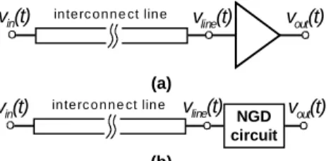
in te rc o n n e ct lin e vin(t) vline(t) vout(t) (a) in te rc o n n e ct lin e vin(t) vline(t) vout(t) NGD circuit (b)
Fig. 1. Interconnect line ended by: (a) a repeater/ (b) an NGD circuit.
To cope with this technological problem, a technique of delay reduction has been introduced in [7-9] using a repeater as schematized in Fig. 1(a). To make more understandable this concept, let us consider a voltage level, V0. Reminding that
according to a threshold level, VT, a repeater consists in
generating an output with either low or high level:
⎩ ⎨ ⎧ ≥ < = T line T line out V t v if V V t v if t v ) ( ) ( 0 ) ( 0 . (1)
Of course, this technique is inadequate when for example, the signal, vline(t) is highly attenuated and lower than VT. For this
reason, the equalization technique using negative group delay (NGD) active circuit (Fig. 1(b)) was proposed [10-13]. As stated in [11], this NGD equalization technique is ideally aimed at generating an output most likely to the input (vout(t)≈vin(t)). In other word, assuming Gline(s) and
GNGD(s), the interconnect- and the NGD- transfer functions
respectively, it enables to fit that one of the whole structure close to unity: 1 ) ( ) ( 1 ) ( / ) (s V s ≈ ⇔ G sG s ≈ Vout in NGD line . (2) It implies that: ) ( / 1 ) (jω G jω GNGD ≈ line , (3) and τNGD(ω)≈1/τline(ω). (4)
Knowing that Gline(jω) <1 and τline(ω)>0, to achieve this
equalization process, the conditions, GNGD(jω) >1 and 0
)
(ω <
τNGD what justifies logically the use of the NGD
active circuit are expected. As seen in Fig. 2, this NGD circuit is composed of a field effect transistor (FET) fed back with an RL series network. To simplify the calculations, the low frequency model of this transistor has been considered.
gmVgs Rds
FET
R L R L
Vgs
FET
Fig. 2. NGD active cell: FET fed back with an RL series network.
According to the circuit and system theory, losses compensation induced by the gain of the active circuit and an
interconnect group delay reduction can be achieved due to the NGD effect.
The remainder of this paper is structured as follows. In section 2, the theory of RC-line model and the proposed NGD active circuit is recalled prior to describing analytically the interconnect equalization. The next section is consecrated to the validation of the presented technique. It explains the design process of the RC-NGD compensator and explores the measured frequency- and time-domain results. The last section concludes this paper.
2. Theoretical Recalls
To simplify the theory and let us consider that interconnects are modeled by RC-lines as illustrated in Fig. 3.
FET vi Rs Rldx Cldx Rldx vo d R L Cldx
Fig. 3. Gate with output resistance, Rs driving an RC-interconnect line
cascaded with an NGD cell.
2.1. RC-line theory
As reported in [7-8], the considered RC-model presents a transfer function given by:
) sinh( ) cosh( ) ( s C R d s C R s C R d R R s G l l l s l l l l RC + = . (5)
Regarding the first order MacLaurin series expansion of the denominator, this quantity will be reduced as follows:
ds C d R R s G l l s RC ) 2 / ( 1 1 ) ( + + = . (6)
This form of transfer function allows considering an equivalent lumped element RC-circuit with a total resistance and capacitance:
RT = Rs + Rld/2, (7)
and CT = Cld. (8)
In this case, the Elmore 50% propagation delay [4] is written as:
TRC = RTCT = (Rs + Rld/2) Cld. (9)
Furthermore, according to the expression (6), this RC-line exhibits a group delay always positive:
2 ) ( 1 ) ( ) ( ω ω ω ω τ RC RC RC RC T T j G + = ∂ ∂∠ − = . (10)
2.2. Recall on the NGD circuit theory
As established in [7], the NGD cell shown in Fig. 1 presents a transfer function expressed as:
Ls R R Ls g R g R s G ds m m ds NGD + + − − = (1 ) ) ( . (11)
It is worth reminding that at very low frequency (ω≈0), this cell exhibits a gain and a group delay defined as:
R R R g R G ds m ds NGD + − = 1 ) 0 ( , (12) ) )( 1 ( ) 1 ( ) ( 0 g R R R R g L j G ds m ds m NGD NGD − + + = ∂ ∂∠ − = ≈ ω ω ω τ .(13)
It means that in base band frequency, losses compensation (GNGD(ω)>1) and NGD (τNGD(ω)<0) can be achieved
under the condition:
R > 2Rds/(gmRds – 1). (14)
2.3. Analytical approach of the proposed RC-line equalization
As stated in [7-8], thanks to the NGD function, interconnect line delay reduction can be realized by considering the configuration shown in Fig. 3. The relevance of this technique is theoretically predicted by the propagation delay expression of this configuration:
] ) 1 [( gmRT ngd TRC T =α + τ + , (15) where 1 ) 1 ( + < + + + = R g R R R R R m T ds ds α . (16)
If τNGD<0, T is undoubtedly lower than the RC-propagation delay described by (9). Moreover, knowing the RC-line parameters Rl, Cl and d, we propose the R- and L-synthesis
formulas in order to realize the equalization of gain and group delay at very low frequency:
1 ) 1 ( 2 − + + = ds m ds m T ds R g R g R R R , (17) 1 ) ( ) )( 1 ( 2 + + + + − = ds T m T ds m RC ds m R R g R R g T R R R g L . (18)
These synthesis formulas lead us naturally to experimental investigation devoted in the next section.
3. Experimental Validation of the Proposed Technique
To validate this equalization technique, prototypes of RC-, NGD- and RCNGD-circuits have been designed and tested
both in frequency- and in time-domains. We underline that along this section, the presented design process and simulations were performed with ADS designer/simulator from Agilent.
3.1. Design Process
To avoid, the eventual disruptions caused by the bias network at low frequency, the FET was biased through application of an improved active-load technique. We use the PHEMT/ATF-34143 from Avago Technology because its characteristics, gm = 226 mS and Rds = 27 Ω which are
extracted from the non-linear model, were well suited for this demonstrator of effects equalization. For the given RC-parameters, the RL NGD-circuit values were synthesized via the expressions (17) and (18). Then, accurate frequency responses are obtained through circuit simulations (lumped components and non linear FET model). A final slight optimization was run with the available lumped component values. The layout of the hybrid planar circuit is printed on a FR4 substrate of permittivity, εr =4.3, and thickness,
h = 800 µm as depicted in Fig. 4. FET drain gate FET gate dr a in
V
d R L Ro Cb Cb Rc C 17 . 00 m m 2 2 . 8 5 m m input output s ubs tr a te F R 4 p e rm it ti v ity : ε r = 4. 3 thi c k nes s : h = 80 0 µ mFig. 4. Layouts of the tested RCNGD-circuit using a PHEMT ATF-34143
(Vgs = 0V, Vd = 3V, Id = 110 mA), for Rc = 33 Ω, C = 680 pF,
and R = 56 Ω, Ro = 10 Ω, L = 220 nH, Cb = 100 nF.
3.2. Experimental Results and Discussions
It is emphasized that the frequency and temporal results examined in this subsection were recorded from an R&S
ZVRE 9kHz-4GHz vector network analyzer and a 2 Gs/s LeCroy digital oscilloscope, respectively.
3.2.1. Frequency Results
(a)
Fig. 5(a). Measured magnitudes of the RC-, NGD- and RCNGD-circuits.
(b)
Fig. 5(b). Measured group delays of the RC-, NGD- and RCNGD-circuits.
As plotted in Fig. 5(a), the measured magnitude, G(f)dB of
the overall circuit is kept within -10 and 0 dB up to 80 MHz and close to 0 up to 40 MHz. It is worth noting that the total magnitude and group delay values are different from the sum of the individual magnitudes because of a possible mismatch between the RC and NGD parts. The group delay of the whole circuit, τ(f), is not fully cancelled (Fig. 5(b)), but it is kept below 4 ns due to the NGD circuit. An absolute higher NGD value could be theoretically obtained, but a compromise between NGD value, NGD bandwidth and gain flatness has to be found to minimize overshoot or ripple in time-domain. 3.2.2. Time Domain Results
SIGNAL GENERATOR DATA sync. 0 0 0 0 0 0 0 0 0 1 0 0 0 0 0 0 0 0 0 0 0 0 0 0 0 0 0 0 0 0 0 0 0 0 0 0 0 0 0 0 0 0 0 0 0 0 0 0 b i n a r y s e q u e n c e DIGITAL OSCILLOSCOPE CH1 CH2 s y n c h r o . s i g n a l input signal cable L1 cable L2 SIGNAL GENERATOR DATA DIGITAL OSCILLOSCOPE CH1 CH2 output signal cable L1 cable L2 sync. (a) (b ) b i n a r y s e q u e n c e 0 0 0 0 0 0 0 0 0 1 0 0 0 0 0 0 0 0 0 0 0 0 0 0 0 0 0 0 0 0 0 0 0 0 0 0 0 0 0 0 0 0 0 0 0 0 0 0 D.U.T s y n c h r o . s i g n a l
Fig. 6. Schematic diagram of the experimental setup: (a) input and (b) output signal recording.
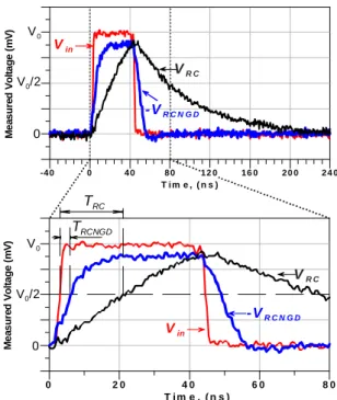
The executed temporal measurement setup is summarized in Fig. 6. Noticed that the square wave pulse is delivered, at the highest rate available, by the baseband data output of a vector signal generator (R&S SMJ 100A). This digital pulse has a 25-Msym/s rate corresponding to a 40-ns width and an amplitude
V0 = 1V. As explained in Fig. 6, to avoid cable and connector
influences, we proceeded systematically in two steps and recorded, at first, the input and then the output signals (connected on CH1) by using the same synchronization reference signal (connected on CH2). We, thus, monitored the input pulse, Vin, the RC- and RCNGD-circuit output ones VRC,
VRCNGD which are resynchronized by using the reference
signal and plotted in Fig. 7. Compared to VRC, the output
VRCNGD waveform is reshaped and less distorted. The
RC-circuit provides a degraded output leading edge with
TRC ≈ 18.50 ns. Hence, the NGD circuit compensation allowed
a reduction of both parameters by leading to trRCNGD ≈ 10 ns
and TRCNGD ≈ 2.50 ns, which means relative reductions of
71.4% (1-trRCNGD/trRC) and 86.5% (1-TRCNGD/TRC). In addition,
as illustrated at the top of Fig. 7, the trailing edge is strongly enhanced. This point is worth being noted when an enhancement of data rate is expected from application of this technique. M e as u red V o lt a g e ( m V) T i m e , ( n s ) V0 2 4 0 2 0 0 1 6 0 8 0 4 0 0 -4 0 Vin VR C -VR C N G D V0/2 0 T i m e , ( n s ) M e as u red V o lt a g e ( m V) 2 0 4 0 0 6 0 8 0 TRC TRCNGD Vin - VR C N G D VR C V0 V0/2 0 1 2 0
Fig. 7. Time-domain responses with an input square pulse (25-Msym/s rate, 2 ns rise- and fall-times) and zoom on two times of the symbol duration.
3.2.3. Remarks between Repeater and NGD Active Circuit It is interesting to underline that as reminded aforesaid, regenerative repeaters characterized by their threshold voltages, VT are sometimes used. Based on the configuration
shown in Fig. 1(a), deeming the degraded voltage, VRC plotted
in Fig. 7, the lowering level of VT would also shortening the
rise time but similarly, it would increase also the fall time. Thus, this proposition is detrimental to the bit duration. So, it is not actually consistent for systems with high data rate. However, to control simultaneously time delay and back/front edges, a dual threshold voltage repeater of course, with a greater complexity could be proposed. Otherwise, another suggestion could be: “why do not simply amplify before switching to the logical level?” This proposal idea allows also the improvement of the raising edge but it contributes to change again the data duration.
4. Conclusions
A new technique of interconnects (restricted to RC-line) effects equalization is investigated and validated. It consists of cascading the line and an NGD active circuit. It is evidenced theoretically and experimentally that this technique allows enhancing the integrity of the signals degraded and especially the reduction of the propagation delay. To achieve a complete validation and to check the efficacy of the theoretical
predictions, the fabricated devices were tested. Indeed, in frequency-domain, the equalization of the RC-circuit magnitude response and the reduction of its group delay were both evidenced. In time-domain, for a 25 Msym/s-rate signal, an excellent reshaping of the degraded signal wave form was obtained. In addition, these measurements confirmed a significant shortening of the rise-time and propagation delay of the distorted signal.
In the continuation of this work, we plan an implementation in MMIC technology. To overcome the eventual difficulty of self integration, investigation on an innovative topology of NGD circuit without inductance is currently in progress.
References
[1] International Technology Roadmap for Semiconductors.
http://www.itrs.net
[2] Rabay, J. M., “Digital Integrated Circuits, A Design
Perspective,” Prentice-Hall (Englewood Cliffs, NJ:1996).
[3] Deutsch, A, “High-Speed Signal Propagation on Lossy Transmission Lines,” IBM J. Res. Develop., Vol. 34, No. 4 (Jul. 1990), pp. 601-615.
[4] Elmore, W. C., “The Transient Reponse of Damped Linear Networks,” J. Appl. Phys. Vol. 19, (Jan. 1948), pp. 55-63. [5] Wyatt, J. L., “Circuit Analysis, Simulation and Design.
North-Holland,” The Netherlands: Elsiever Science (1978).
[6] Kahng, A. B. and Muddu, S., “An Analytical Delay model of RLC Interconnects,” IEEE Trans. Computed-Aided
Design, Vol. 16 (Dec. 1997), pp. 1507-1514.
[7] Adler, V. and Friedman, E. G., “Repeater Design to Reduce Delay and Power in Resistive Interconnect”, IEEE
Trans. Circuits Syst. II, Analog and Digital Signal Processing, Vol. 54, No. 5, (May 1998), pp. 607-616.
[8] Ismail, Y. I. and Friedman, E. G., “Effects of Inductance on the Propagation, Delay and Repeater Insertion in VLSI Circuits,” IEEE Trans. VLSI Sys., Vol. 8, No. 2, (Apr. 2000), pp. 195-206.
[9] Bartolini, M., Pulici, P., Stoppino, P. P. and Campardo, G., “A Reduced Output Ringing CMOS Buffer,” IEEE
Trans. Circuits Syst. II, Exp. Briefs, Vol. 54, No. 2, (Feb.
2007), pp. 102-106.
[10] Solli, D. and Chiao, R. Y., “Superluminal Effects and Negative delays in Electronics and their Applications,”
Phys. Rev. E, Issue 5, (Nov. 2002).
[11] Ravelo, B., “Negative Group Delay Active Devices: Theory, Experimental Validations and Applications,”
Ph.D. thesis, chap. 8, Lab-STICC, UMR CNRS 3192,
University of Brest, France, (Dec. 2008).
[12] Ravelo, B., Pérennec, A. and Le Roy, M., “Equalization of Interconnect Propagation Delay with Negative Group Delay Active Circuits,” 11th IEEE Workshop on SPI, Genova, Italy, (May 2007), pp. 15-18.
[13] Ravelo, B., Pérennec, A. and Le Roy, M., “Application of Negative Group Delay Active Circuits to Reduce the 50% Propagation Delay of RC-Line Model,” 12th IEEE