Vapor Phase Doping: an Atomic Layer Deposition approach to n-type doping
in classical Chemical Vapor Deposition epitaxy
S. Takeuchi*, N. D. Nguyen, F. Leys, R. Loo, T. Conard, W. Vandervorst, and M. Caymax
IMEC, Kapeldreef 75, B-3001 Leuven, Belgium
*
Phone : +32 16 28 7743, Fax : +32 16 28 1706, E-mail : [email protected]
Atomically-controlled processing and modulation doping technology are required for the realization of advanced Si electronic devices such as heterojunction bipolar transistors and three-dimensional or modulation doped field effect transistors. In these cases, the atomic layer deposition (ALD) technique is an efficient way to achieve precisely controlled doping profiles. So far, vapor phase doping (VPD) with boron and phosphorus (P) as the dopant in Si or SiGe epitaxy has been reported by low pressure chemical vapor deposition (LPCVD) [1,2]. In the present work, we performed VPD with P and arsenic (As) with various growth conditions by atmospheric pressure (AP) CVD. Shallower as-deposited dopant profiles are expected at AP. Because P and As have the tendency to easily desorb even at low temperature, as shown here below, a standard thermal anneal step is not suitable to drive the dopants into the substrate. An alternative is the epitaxial incorporation of the dopant atoms under one or more successive monolayers (MLs) of Si. Therefore, we also studied the growth kinetics of Si on the dopant-covered Si. The VPD on blanket 200 mm Si(001) wafers was performed at 400~600oC in 1 bar of N2 using phosphine (PH3) or arsine (AsH3) diluted to 0.1 % in H2 in a standard horizontal cold wall, load-locked, ASM Epsilon
TM 2000 reactor. The PH3 or AsH3/H2 flow condition is 50~200 standard cubic centimeters per minute during 1~100 minutes. A Si cap was subsequently deposited on the dopant-covered Si at 650oC or at 575oC using SiH4 at reduced pressure. The total dose was determined by X-ray photoemission spectroscopy (XPS) and secondary ion mass spectroscopy (SIMS). The electrically active dose was obtained by a four-point-probe (FPP) method combined with well-known carrier mobility data [3].
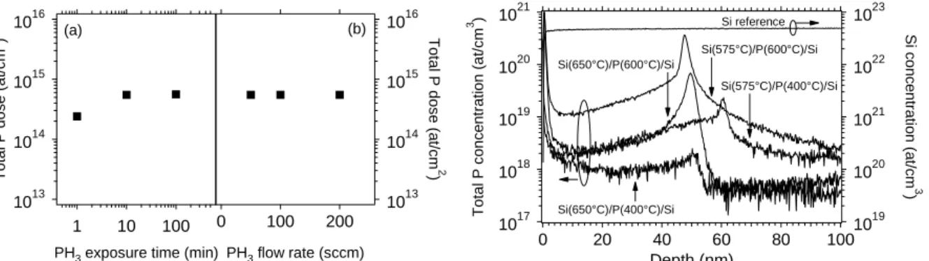
The P doses as function of the PH3 exposure time and flow rate in P/Si-substrate structures are shown in Fig. 1(a) and Fig. 1(b). The P dose saturates to about 1 ML at given conditions and is therefore self-limiting, i.e. perfectly in line with classical ALD. The total and electrically active P doses in Si-cap/P/Si-substrate structures have been studied also as function of the growth conditions. It was found that the temperatures of the VPD step and of the Si-cap have a strong influence on the dopant doses. The Si growth rate on P-covered Si was ~20% lower than that on Si. Figure 2 shows the P SIMS profiles for various growth conditions. The hydrogen coming from dissociative adsorption of PH3 desorbs above 450oC. Therefore, the P dose increases with increasing VPD temperature as shown in Fig. 2 [1]. In contrast, since P tends to desorb above 600oC, a low P peak with the Si-cap grown at 650oC was obtained compared with the Si-cap grown at 575oC. The total and active P doses in the Si-cap(575oC)/P(600o C)/Si-substrate structure were estimated to be 2.6×10¹⁴ and 1.6×1014 cm-2, respectively. Arsenic data will be shown and discussed at the conference.
ALD has been achieved by the VPD process. Present results allow to evaluate the feasibility of our VPD process to fabricate controlled doping profiles.
[1] B. Tillack, Thin Solid Films 318, 1 (1998). [2] J. Murota, M. Sakuraba and B. Tillack, Jpn. J. Appl. Phys. 45, 6767 (2006). [3] S. M. Sze, Physics of Semiconductor Devices 2nd edition, J. Wiley and Sons, 32 (1981).
1017 1018 1019 1020 1021 Total P co nce n tra ti on ( a t/cm 3 )
Fig. 1. Total P dose as function of (a) PH3 exposure time and
(b) flow rate by angle-resolved XPS.
Fig. 2. SIMS profiles of as-deposited P in Si/P/Si structures.
1013 1014 1015 1016 Total P dose (a t/cm 2 ) 200 100 0 PH3 flow rate (sccm) 1013 1014 1015 1016 To tal P dose (a t/cm 2 ) 1 10 100
PH3 exposure time (min)
(a) (b) 20 40 0 De 60 80 100 pth (nm) 1019 1020 1021 1022 1023 Si c o nc en tr a tion (at /c m 3 ) Si(650°C)/P(600°C)/Si Si(650°C)/P(400°C)/Si Si(575°C)/P(600°C)/Si Si(575°C)/P(400°C)/Si Si reference