HAL Id: hal-01069400
https://hal.archives-ouvertes.fr/hal-01069400
Submitted on 29 Sep 2014
HAL is a multi-disciplinary open access
archive for the deposit and dissemination of sci-entific research documents, whether they are pub-lished or not. The documents may come from teaching and research institutions in France or abroad, or from public or private research centers.
L’archive ouverte pluridisciplinaire HAL, est destinée au dépôt et à la diffusion de documents scientifiques de niveau recherche, publiés ou non, émanant des établissements d’enseignement et de recherche français ou étrangers, des laboratoires publics ou privés.
On-chip grating coupler array on the SOI platform for
fan-in/fan-out of multi-core fibers with low insertion loss
and crosstalk
Yunhong Ding, Feihong Ye, Christophe Peucheret, Haiyan Ou, Yutaka
Miyamoto, Toshio Morioka
To cite this version:
Yunhong Ding, Feihong Ye, Christophe Peucheret, Haiyan Ou, Yutaka Miyamoto, et al.. On-chip grating coupler array on the SOI platform for fan-in/fan-out of multi-core fibers with low insertion loss and crosstalk. 40th European Conference on Optical Communication (ECOC 2014), Sep 2014, Cannes, France. paper We.1.1.3, �10.1109/ECOC.2014.6964081�. �hal-01069400�
ECOC 2014, Cannes - France We.1.1.3
On-chip Grating Coupler Array on the SOI Platform for
Fan-in/Fan-out of Multi-core Fibers with Low Insertion
Loss and Crosstalk
Yunhong Ding(1), Feihong Ye(1), Christophe Peucheret(2), Haiyan Ou(1),
Yutaka Miyamoto(3), and Toshio Morioka(1)
(1) DTU Fotonik, Department of Photonics Engineering, Technical University of Denmark,
2800 Kgs. Lyngby, Denmark, yudin@fotonik.dtu.dk
(2) FOTON Laboratory - CNRS UMR 6082, ENSSAT, University of Rennes 1, 22300 Lannion, France. (3) NTT Network Innovation Laboratories, NTT Corporation, Yokosuka, Kanagawa, 239-0847, Japan.
Abstract We design and fabricate a compact multi-core fiber fan-in/fan-out using a fully-etched grating
coupler array on the SOI platform. Lowest coupling loss of 6.8 dB with 3 dB bandwidth of 48 nm and crosstalk lower than -32 dB are demonstrated.
Introduction
The communication capacities of single mode fiber (SMF)-based optical transmission systems have been rapidly pushed towards their theoretical limit1 by the fast growing traffic demand these years. Space-division multiplexing (SDM) based on multi-core fibers (MCFs) has been demonstrated to be a promising technology to further increase the communication capacity over a single fiber. By introducing uncoupled multiple cores in a single fiber, large communication capacities with long transmission distances have been reported 2-6. One important component for MCF based SDM technology is a compact and efficient MCF fan-in/fan-out (FI/FO) device with low coupling loss and large bandwidth. Several FI/FOs schemes have been proposed, including free space based coupler6, three dimensional (3D) waveguides fabricated by ultrafast laser inscription7, physical-contact type FI/FO8, etc.
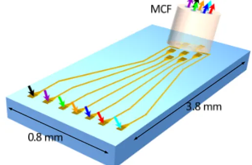
In this paper, we demonstrate a compact on-chip 7-core fiber FI/FO using a fully-etched apodized grating coupler array on the silicon-on-insulator (SOI) platform, as shown in Fig. 1. Coupling loss as low as 6.8 dB with 3 dB bandwidth of 48 nm and less than 3 dB coupling loss variation between spatial channels were achieved. It is a promising technology thanks to its potential for integration of many FI/FO couplers and other functionalities such as switching matrices on the same chip.
Grating coupler design
An SOI chip enabling coupling from 7 standard SMFs (SSMFs) to one 7-core MCF using grating couplers is proposed, as shown in Fig. 1. The grating couplers, identical at both ends of the circuit, are designed and optimized for coupling to SSMFs. A silica-clad fully-etched silicon photonic crystal (PhC) grating coupler with bonded bottom mirror on a silicon carrier wafer is proposed, as depicted in Fig. 2. There are
Fig. 1: Schematic of the grating coupler-based FI/FO.
three advantages for the proposed design. Firstly, the fabrication process can be simplified by using a fully-etched design so that the grating couplers can be simultaneously fabricated with the rest of the circuit9. Secondly, a high coupling
efficiency (CE) can be achieved thanks to the bonded metal mirror. Finally, both upper and lower cladding thicknesses can be precisely optimized by bonding technology. The thickness of the top silicon device layer is 250 nm. In order to achieve an apodized grating coupler diffracting a Gaussian field profile, artificial materials are introduced for the scattering units, with refractive indices ni and lengths of
scattering units li changed along the grating9.
SiO2 is used as upper and lower cladding
material with thicknesses of hu and hd,
Fig. 2: Structure of the grating coupler.
ECOC 2014, Cannes - France We.1.1.3 ni li (n m ) CE CE
Fig. 3: (a) Designed li and ni distributions of the grating
couplers. Simulated coupling efficiency as a function of (b) hd , with hu=1000 nm, and (c) wavelength, with hd=1600 nm,
and hu=1000 nm.
respectively. A 100 nm titanium (Ti) mirror is introduced below the lower cladding. Another layer of SiO2 is introduced beneath the Ti mirror
and is bonded to the silicon carrier wafer using a benzocyclobutene (BCB) layer. The coupling angle is designed to be 15º. The width of the artificial material slots is fixed to be 345 nm, and the scattering strength and coupling angle are tuned by optimizing ni and li. The distributions of
ni and li of the grating coupler are designed, as
shown in Fig. 3(a), so that a Gaussian output field profile with a beam radius of 5.2 µm is synthesized from the grating with a coupling angle of 15º at 1550 nm. PhCs with triangular lattices can then be used for the artificial material slots, and the hole size for the PhCs can be determined by the effective index approximation9. The coupling efficiency of the
transverse electric (TE) mode is then calculated by a 2D eigen-mode expansion method (EME) as a function of hd with hu set to 1000 nm, as
shown in Fig. 3(b). The coupling efficiency depends periodically on hd, and reaches a local
maximum at hd= 1600 nm. With hd=1600 nm
and hu=1000 nm, the coupling efficiency is then
calculated as a function of wavelength, as shown in Fig. 3(c). A peak coupling efficiency of
Fig. 4: (a) Fabricated device. (b) Details of the grating
coupler array for directly coupling with a MCF. (c) Scanning electron microscopy (SEM) image of the apodized PhC
grating coupler.
81% (corresponding to 0.91 dB coupling loss) is predicted with a 3 dB bandwidth of 74 nm.
Device fabrication and characterization
In order to validate our concept, the device was fabricated on a commercial SOI sample with top silicon thickness of 250 nm and buried silicon dioxide (BOX) of 3 μm. A single step of standard SOI processing, including e-beam lithography and inductively coupled plasma (ICP) etching was first used to fabricate the grating coupler and silicon waveguides simultaneously. An 800 nm thick layer of SiO2 was then deposited
on top of the chip. Another 800 nm boro-phosphosilicate (BPSG) glass was deposited and annealed in nitrogen at 950ºC for 30 minutes in order to planarize the chip surface. Afterwards, a 100 nm thick Ti layer was deposited on top of the BPSG. Then, about 2 μm BCB layer was spun on both the sample and silicon carrier wafer. The sample was then flip-bonded on the silicon carrier wafer and thermally cured in an oven. Finally the substrate of the chip was removed by ICP fast etching.
Fig. 4 shows details of the fabricated device. The grating coupler is constructed by PhC based scattering slots with waveguide width of 12 µm, as shown in Fig. 4(c). The layout of the output grating couplers correspond to that of the cores of the MCF, with the same pitch of 49 µm, as shown in Fig. 4(a) and 4(b). In addition, 45º-slants with measured low insertion loss of
Fig. 5: Measurement setup of the grating coupler array-based on-chip MCF FI/FO.
ECOC 2014, Cannes - France We.1.1.3
0.05 dB, are introduced to change the light beam propagation direction so that the 500 µm long taper (from 12 µm for the grating to 450 nm for the silicon single mode waveguide) can be placed outside the grating coupler array, as shown in Fig. 4(b).
The coupling loss from our device to an MCF with core pitch of 49 µm and effective area of 110 µm2 at 1550 nm was measured for each core. Fig. 5 shows the measurement setup. The device was mounted on a rotatable stage. Continuous wave (CW) laser light from a tunable laser source (TLS) was polarization-tuned by a polarization controller (PC), so that the light was launched to the input grating coupler on the TE mode. The MCF was mounted to a fiber holder with input angle of 15º. The stage was then horizontally rotated until all the grating couplers were well aligned with the corresponding cores of the MCF. The output of the MCF was spatially demultiplexed by a free space coupling device10, and the output power from each core was measured by an optical spectral analyzer (OSA). The coupling efficiency of the MCF FI/FO is shown in Fig. 6. It was obtained by subtracting the MCF transmission loss and free space coupling loss from the total link loss (from the grating coupler input to the free space coupling output). A lowest coupling loss of 6.8 dB with 3 dB coupling bandwidth of 48 nm and less than 3 dB coupling loss variation for the different spatial channels were measured. It should be noted that the coupling loss includes the loss of the input grating coupler, propagation loss along the silicon waveguides, insertion loss of the 45º-slant, and loss of the output grating coupler to the MCF. It should also be noted that our alignment method by rotating the stage will lead to non-optimum coupling angle for the MCF, resulting in larger coupling loss. Lower coupling loss can be expected by rotating the MCF instead. In addition, aluminum (Al) can be used instead of Ti for the back mirror to further reduce the coupling loss. Moreover, the effective area of 110 µm2 of each fiber core is larger than that
Couplin
g efficien
cy
(dB
)
Fig. 6: Measured coupling efficiency and crosstalk for the
MCF FI/FO.
of an SSMF, for which the grating coupler was designed, which also results in higher coupling loss. Optimization of the output grating coupler can further reduce the total coupling loss. The crosstalk was also investigated by launching light into input CH1 and detecting light from the
other non-corresponding cores (core 2 to 7) of the MCF. A low crosstalk of -32 dB over a large bandwidth of 100 nm was measured, which is very close to a measured SMF to MCF crosstalk value of -35 dB for the free space coupling device, indicating that the grating coupler array has very low crosstalk.
Conclusions
We have designed and demonstrated a compact MCF FI/FO using a fully-etched grating coupler array on the SOI platform. A lowest coupling loss of 6.8 dB with 3 dB coupling bandwidth of 48 nm and less than 3 dB coupling loss variation between spatial channels were achieved.
Acknowledgement
This work is supported by the Danish Council for Independent Research (DFF–1337-00152 and DFF–1335-00771).
References
[1] T. Morioka, “New Generation Optical Infrastructure Technologies: “EXAT Initiative” Towards 2020 and Beyond,” (invited) Proc. OECC, FT4, Hong Kong (2009). [2] H. Takara et al., “1.01-Pb/s (12 SDM/222 WDM/456
Gb/s) Crosstalk-managed Transmission with 91.4-b/s/Hz Aggregate Spectral Efficiency,” Proc. ECOC, Th.3.C.1, Amsterdam (2012).
[3] B. Zhu et al., “Seven-core Multicore Fiber Transmissions for Passive Optical Network,” Opt. Express, Vol. 18, p. 11117 (2010).
[4] T. Kobayashi et al., “2×344 Tb/s Propagation-direction Interleaved Transmission Over 1500-km MCF Enhanced by Multicarrier Full Electric-field Digital Back-Propagation,” Proc. ECOC, PD3.E.4, London (2013). [5] T. Mizuno et al., “12-core×3-mode Dense Space
Division Multiplexed Transmission over 40 km Employing Multi-carrier Signals with Parallel MIMO Equalization,” Proc. OFC, Th5B.2, San Francisco (2014). [6] J. Sakaguchi et al., “19-core Fiber Transmission of 19 ×
100 × 172-Gb/s SDM-WDM-PDM-QPSK Signals at 305 Tb/s,” Proc. OFC, PDP5C.1, Los Angeles (2012). [7] R. R. Thomson et al., “Ultrafast Laser Inscription of a
121-waveguide Fan-out for Astrophotonics,” Opt. Lett., Vol. 37, p. 2331 (2012).
[8] Y. Abe et al., “Low-loss Physical-contact-type Fan-out Device for 12-core Multicore Fiber,” Proc. ECOC, P.1.7, London (2013).
[9] Y. Ding et al., “Ultrahigh-efficiency Apodized Grating Coupler Using Fully Etched Photonic Crystals,” Opt. Lett., Vol. 38, p. 2732 (2013).
[10] W. Klaus et al., “Free-space Coupling Optics for Multicore Fibers,” IEEE Photon. Technol. Lett., Vol. 24, p. 1902 (2012).
Powered by TCPDF (www.tcpdf.org)