Realizing the diamond annular groove phase masks for the mid
infrared region - five years of successful process development of
diamond plasma etching
Pontus Forsberg*
a, Ernesto Vargas
a, Christian Delacroix
b, Olivier Absil
b, Brunella Carlomagno
b,
Dimitri Mawet
c, Serge Habraken
b, Jean Surdej
b, Mikael Karlsson
aa
Department of Engineering Sciences, Uppsala University, Box 534, 751 21 Uppsala, Sweden;
bDépartement d’Astrophysique, Géophysique et Océanographie, Université de Liège, 17 Allée du
Six Août, B-4000 Liège, Belgium;
cEuropean Southern Observatory Vitacura, Alonso de Cordova
3107, Casilla 19001, Vitacura, Santiago 19, Chile
ABSTRACT
The Annular Groove Phase Mask (AGPM) is a circularly symmetric half wave plate consisting of a circular high aspect ratio sub-wavelength grating. Here we present a method for realizing such structures in diamond. To improve the AGPM performance, antireflective sub-wavelength gratings are etched on the backside of the components, and such gratings are also discussed. Components for the N-band (around 10 µm) and the L-band (around 3.8 µm) have been successfully fabricated. We are currently developing the process further to improve the precision of the gratings and produce an AGPM for the K-band (around 2.2 µm).
Keywords: Gratings, diamond, coronagraphy, microfabrication
1. INTRODUCTION
Diamond is a material with many extreme characteristics. It has a wide transparency window, a high refractive index, is inert to nearly all chemicals and resistant to radiation damage, it is the hardest of all materials, it has the highest thermal conductivity and also a small thermal expansion. Some of these properties make it an interesting material for visible and infrared optics, particularly in challenging environments.
We have been etching optical gratings in diamond for more than a decade and for the past several years have been pushing our processes to achieve the precision required for the annular groove phase mask (AGPM). The AGPM consists of a grating of concentric circular grooves, which acts as a circularly symmetric half-wave plate. Such a component will give rise to an optical vortex, which can be used in a vector vortex coronagraph [1]. For the grating to act as a wave plate and not a diffraction grating it is important that the period is smaller than the light wavelength. Further, very high precision is required in all the grating parameters: depth, line width and wall angles (see figure 1), to unlock the full potential of the grating for coronagraphy. To avoid internal reflections in the diamond substrate, which will otherwise limit the performance of the component, the AGPM also has a sub-wavelength grating on the backside optimized to reduce reflectance.
This paper will first give an overview of sub-wavelength gratings for use as antireflective gratings and wave plates and then describe our fabrication process, with a focus on recent improvements. We will conclude by showing some results and discuss what we hope our latest process development will mean for our next generation of components.
* pontus.forsberg@angstrom.uu.se; phone +46 18 4717235
Advances in Optical and Mechanical Technologies for Telescopes and Instrumentation, edited by Ramón Navarro, Colin R. Cunningham, Allison A. Barto, Proc. of SPIE Vol. 9151, 915119
© 2014 SPIE · CCC code: 0277-786X/14/$18 doi: 10.1117/12.2055475 Proc. of SPIE Vol. 9151 915119-1
Figure 1. Critical grating parameters: period (Λ), width (w) (defined at the top of the grating profile), depth (d) and the sidewall angle (α) (deviation from vertical).
2. SUB-WAVELENGTH GRATINGS
2.1 Gratings in the sub-wavelength regime
When light hits a grating it is usually diffracted, splitting the light into several beams (orders). However, if the period of the grating is small compared to the wavelength of the illuminating light, no diffraction takes place and all the light remains in the zero order (directly transmitted or reflected). The light behaves as if the grating was a continuous medium with optical properties determined by the grating morphology and the properties of the materials making up the grating. By carefully designing the grating, properties such as refractive index and birefringence can be controlled. The grating parameters typically have to be optimized numerically, for example by rigorous coupled wave analysis (RCWA). A cross section of an idealized grating can be seen in figure 1. Determining the proper period (Λ) is simple, it just has to be smaller than the shortest operating wavelength in either material making up the grating (Λ < λ/nmax). The optimal
width (w) and depth (d) have to be calculated numerically and often an error in one can be compensated for (or exacerbated by) the other. Especially the width can be very sensitive and errors of a few tens of nanometers can be deleterious even when the operating wavelength is in the mid-infrared. The sidewalls in a realistic grating are never perfectly vertical. When etching shallow gratings, such as binary antireflective gratings, the effect of the angle (α) is usually small, but when etching deep gratings, for quarter- or half-wave plates, the angle must be known to within a tenth of a degree and accounted for. The walls might not be straight either, but a simple trapezoidal grating like the one in figure 1 is usually a good enough approximation even if the walls are slightly concave or convex.
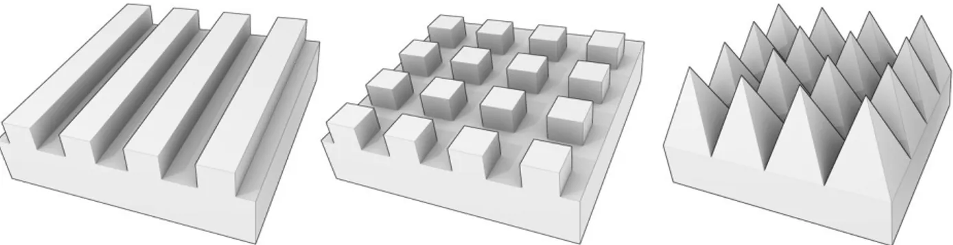
Figure 2. Illustrations of gratings. From left to right: a one dimensional grating, a binary square grating and a pyramidal square grating.
d
Λ w
α
period 4 um, angle 5
1.4
2.2 2.3 2.4 2.5 2.6 2.7 2.8 2.9
width of top (um)
0.995 0.99 0.985 0.98 0.975 0.97 0.965 0.96 0.955 0.95
Figure 3. Illustration of reflections in a film on a substrate. 2.2 Antireflective gratings
Since the refractive index of sub-wavelength gratings can be controlled, they can be used analogously with thin films to reduce the reflectivity of a surface. With the right refractive index (effective refractive index) and film thickness (grating depth), the reflections from the front and back of the film (sub-wavelength grating) can be made to destructively interfere (figure 3), at least for certain incidence angles and wavelengths. Typically square two-dimensional gratings are used for antireflection, to avoid introducing any change of the polarization of the light. The effective refractive index of a sub-wavelength grating lies somewhere in between the refractive indices of the materials making up the grating (here air and diamond). Assuming a simple square binary grating etched in the substrate material (figure 2) and air as the incident medium, the depth of the grating can be calculated from the premise that the two reflected components in figure 3 should be of equal amplitude and opposite phase:
d
=
λ
4 n
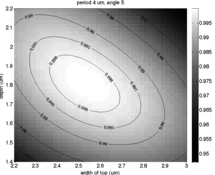
(1)Where λ is the wavelength of light in vacuum and n the refractive index of the substrate material. The width of the raised squares in the grating are not so readily calculated analytically, and if the angle of the sidewall is to be taken into account the depth too can be a little off from equation 1. Figure 4 shows the transmission of 10.6 µm light through a structured air-diamond interface for a range of widths and depths, calculated by RCWA.
Figure 4. RCWA calculations of transmission across an air-diamond interface with a square binary grating. λ=10.6, Λ=4 μm, α=5.
Gratings have two great advantages over thin films for reducing reflection: First, a grating can always be designed with an optimal effective refractive index, whereas a material with a suitable refractive index may not exist for all substrate materials. Second, when a material with a suitable refractive index exists, it may be unsuitable due to poor adhesion, thermal expansion mismatch or even radioactivity (as is the case with thorium tetrafluoride). Since the grating is made from the same material as the substrate, none of these problems occur. A structured surface may however be more prone to fouling and more difficult to clean than a smooth film.
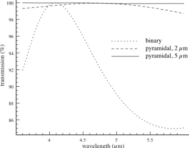
Stepped gratings and sloped structures can be used in the same way as multiple films and gradient refractive indices to improve the bandwidth and incidence angle range for antireflective films. Even for narrow band and normal incidence applications, continuous sloped structures have the advantage of being less sensitive to the grating depth. An optimal continuous structure is deeper than a binary one, thus making it more fragile, but even with a shallow depth a continuous structure can give much better broadband performance than a binary one (figure 5).
Figure 5. RCWA calculations of transmission across a structured air-diamond interface. The grating parameters of the binary grating are Λ=1.5 μm, w=0.975 μm and d=2 μm (with this grating the two reflected components in figure 2 would be 1.5 wavelengths out of phase) and of the pyramidal Λ=1.5 and d=2 or d=5 μm.
2.3 Wave plates
It is intuitively plausible that light polarized parallel to a one-dimensional sub-wavelength grating should experience a different material than light polarized perpendicular to the grating. More generally a two dimensional grating that is not symmetric in the two dimensions, will have different effective refractive indices for the two polarizations (ns and np), and
these can be controlled separately. This ability to tune the birefringence makes sub-wavelength gratings suitable for use as wave plates [2]. The shift in the relative phase between polarizations after passing through such a grating is given by
ΔΦ
s−p= 2
π
d
λ
⎛
⎝
⎜
⎞
⎠
⎟(n
s(
λ
)
− n
p(
λ
))
, (1)An advantage of sub-wavelength gratings as wave plates is that the difference Δn(λ) = ns(λ) – np(λ) can be tuned to be
roughly proportional to the wavelength over a wavelength band, thus making the wave plate quasi-achromatic.
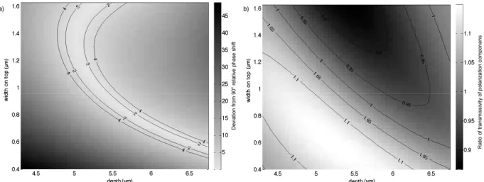
Figure 6a shows the deviation from a quarter wave phase difference between polarizations of 10.6 µm light passing through a one-dimensional grating. As can be seen, there is a continuous arc of possible solutions. A range of solutions is expected since we can control the difference in refractive index and the path through the grating separately by tuning the width and depth. This gives us a chance to optimize something apart from the phase shift; we may for example be concerned with the transmittance for the two polarizations. The ratio between these is mapped in figure 6b.
Ith on top (pm) 90° relative phase shift u, f polarization componens 0.8 0.6 0 .5 5.5 depth (pm) 20 E 3 15 0.8 0.6 0.4 6.5 4.5 o E 0.95 2 0.9 0.66 0.65 0.64 0.63 0.62 0.61 o 3 0.6 0.59 0.58 0.57 4.9 5 5.1 depth (um) 5.2 5.3 5.4 5.5
Figure 6. RCWA results for a quarter wave plate in diamond for 10.6 µm wavelength. (a) The deviation (in degrees) from a quarter wave relative phase shift between polarizations. (b) The ratio of transmitted flux between polarizations. Λ=4 μm, α=2.75.
2.4 The AGPM
A distinct advantage of sub-wavelength gratings as wave plates is that the direction of the grating can be varied freely across a surface, allowing for components that might otherwise be very difficult to produce. The Annular Groove Phase Mask (AGPM) is one such component. By etching the grating as concentric circles, a circularly symmetric half wave plate is formed. This gives rise to an optical vortex with a singularity at its center, which can be used attenuate starlight in a vector vortex coronagraph. The null depth (N) of such a coronagraph, defined as the ratio of the signal intensity when the input beam is centered on (Icoro) and off (Ioff) the coronagraph, is given by
N(
λ
)
= I
coroI
off=
(1− q(
λ
))
2+
ε
(
λ
)
2q(
λ
)
(1+ q(
λ
))
2 , (1)where ε is the phase error (relative to π) and q is the flux ratio between polarization components [3]. An optimal AGPM should minimize the null depth over a given wavelength band. Figure 7 shows the mean null depth mapped for a range of grating widths and depths. As can be seen, there is a range of reasonably good solutions along a diagonal in the map. This will be important for the fabrication, as we will see in the next section. For now, we can note that the precision required in width is around ten times greater than in depth.
Figure 7. AGPM null depth map. Averaged over the L-band, 3.4-4.15 µm. Λ=1.42 µm, α=3.15°. RCWA calculation.
\,
-. ItCttifil
Iffrffm
g 3. FABRICATION PROCESS
Our fabrication process can be divided into the following steps: pattern drawing on silicon wafer, deposition of masking layers on diamond substrate, replication of pattern to top of masking layers, etching of mask layers and etching of diamond. Finally, remaining mask material is removed in strong acids. This is illustrated in figure 8. Control and measurement steps are also required, particularly between etching the mask and etching the diamond. For components etched on both sides, a protective film is deposited on the grating before the process is repeated on the backside of the substrate. The process has been described in some detail in [4], so the focus here will be on recent improvements.
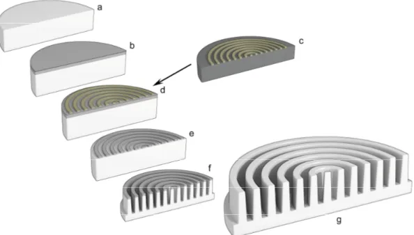
Figure 8. Fabrication process flow. a) diamond substrate, b) masking layers deposited, c) patterned master wafer, d) pattern transferred to the diamond, e) mask etched, f) diamond etched, g) remaining mask stripped, grating finished.
3.1 Pattern design and master wafer fabrication
When designing the pattern to be written on the master wafer, it is important to know how much the lines or squares might shrink or grow during the processing, so that this can be compensated for. Previously, when producing components for the N-band and also for the first L-band components, we have had shrinkages of around 300 nm in line width, partly from the pattern transfer step and partly from the mask etching. To compensate for these we designed the master pattern with lines that were 300 nm wider than the target width. This was obviously not possible when going to shorter wavelengths, there just was not enough room between the lines to allow for that much extra width. With recent improvements to the processing however (see the respective sub-sections), shrinkage has been minimized and the master can be designed with the exact pattern we want to etch in the diamond.
Once designed, the master pattern is produced with e-beam lithography or, for larger grating periods, laser writing, in polymer resist approximately 500 nm thick.
3.2 Masking layer deposition
Metal masking layers are deposited by magnetron sputtering. For deep gratings, such as the AGPM, three layers of mask is used: A thick Al layer, a Si layer and a thinner Al layer on top. For the L-band AGPM the layer thicknesses are around 800 nm, 300 nm and 100 nm respectively. For shallower gratings, like binary antireflective gratings, a single Al layer is used, usually around 200 nm thick.
3.3 Replicating the pattern from the master to the diamond
E-beam lithography is a slow and expensive process. To avoid having to write the pattern on every substrate, we have chosen to replicate it from a master wafer instead. Previously we have used nanoimprint lithography to replicate the pattern on the master wafer. This worked well for the N-band, but we had difficulties when working with finer gratings. Due to the small size and less than perfect smoothness (there can be steps of a few tens of nm between diamond grains) of the diamond substrates, we chose to use a soft stamp. In the finer gratings we have noticed that this gave rise to a reduction in line width and that some variations in width were common, especially around the center of the component. Recently we have started working with a solvent assisted micro molding (SAMIM) technique adapted from [5]. This method is somewhat more time consuming than nanoimprinting and can certainly do with some further tuning, but we have achieved very good fidelity in the replicated patterns with nearly no difference in line widths compared to the master pattern.
3.4 Etch processes
All our etching is done using inductively coupled plasma in a system from PlasmaTherm. The first Al layer is etched using chlorine chemistry with a gas mixture of Cl2 and BCl3. The Si layer is then etched using a mixture of SF6, C4F8 and
Ar. By adding C4F8 to the plasma Si can be etched with nearly no etching. Previously we have used some
under-etching in the Si etch to remove small defects and tune the line width. While this worked well for larger patterns, fluctuations in etch rate made it too difficult to control the amount of under-etching for finer gratings. The new Al-etch recipe is also much less aggressive to the thin Al mask, so that the top masking layer can now be made even thinner. Alternating steps of Cl2/BCl3 plasma and oxygen plasma are used to etch the thick Al mask. The oxygen plasma step
oxidizes the sidewalls, giving a much more vertical profile to the etching. This vertical mask profile is important to avoid direct redeposition of mask material during diamond etching.
After the mask has been etched, it is studied using SEM to measure the line width. As can be seen in figure 7, the optimal etch depth depends strongly on the line width. By carefully measuring the width of the Al mask, the proper etch depth can be determined for every sample.
Diamond is etched in an O2/Ar plasma. A high capacitively coupled power during this etching gives a lot of high-energy
ions impacting the surface. Together with the Ar in the gas mixture, this leads to a strong physical component of the etching, necessary for achieving a high etch rate in diamond. Because the etch rate in diamond depends strongly on the width and depth of the etched grooves, two test pieces patterned with the same grating are etched before the component to determine the etching time.
During diamond etching material is sputtered from the sides of the mask and deposited on the opposite side of the groove (figure 9). Particularly when etching gratings with small periods, this redeposition contributes to higher sidewall angles in the diamond. We are currently exploring ways of reducing this redeposition, to allow deeper gratings to be etched. As noted in section 2.2 above, structures with a continuous profile can be useful for broadband antireflective gratings. To fabricate gratings like these we have also developed processes for producing more sloped sidewalls in diamond, mainly by adding some SF6 to the plasma during diamond etching. This increases the etch rate in the Al mask while inhibiting
redeposition. As the mask slowly withdraws, a more pyramidal structure is formed. This is described in detail in [6].
Figure 9. Cross section of an AGPM grating for the L-band before and after stripping the remaining mask and redeposited material. The redeposition sticks close to the top of the groove and slowly closes it, restricting the maximum etch depth.
4. RESULTS AND CONCLUSIONS
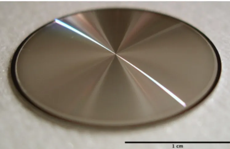
Already we can make gratings with great precision in all parameters. The sidewalls in our current gratings are around 3° off vertical, less for larger period gratings and a more for small period ones, but the variations are within a couple of tenths of a degree. The error in line width can typically be kept within 50 nm. The precision in depth depends on how deep the grating is, but the error is within 1-2% or less. Since the target depth can be chosen after the mask is etched and the line width known, error in width is not as critical to the function of the AGPM as it might otherwise be. We have etched gratings with good homogeneity across diamond surfaces 2 cm in diameter (figure 10).
Figure 10. Photo of a 2 cm diameter AGPM grating. The picture is taken before removing the remaining Al mask after etching.
So far we have successfully produced working AGPM components for the L- and N-band (around 3.5-4.1 µm and 11-13.2 µm respectively). A cross section of an L-band grating can be seen in figure 9 and figure 11 shows some views of an N-band grating. The optical performance has been good [3, 7], but particularly for the L-band we are confident that we can improve the performance further. Internal reflections in the component remain a problem and improved antireflective gratings will reduce those. Since a few nanometers difference in line widths of the AGPM grating can
N
affect the performance of the component, an element of chance will always remain in the processing. The improvements to the processing described above are chiefly aimed at greater reproducibility in mask line width, reducing the error from around ±50 nm to ±20. This should greatly improve the yield of good components and thereby increase the likelihood of producing an excellent one.
Figure 11. Views of AGPM gratings for the N-band. On the left a view of the center, inclined 18°, and on the left a cross section.
ACKNOWLEDGEMENTS
The research leading to these results has received funding from the European Research Council under the European Union's Seventh Framework Programme (ERC Grant Agreement n.337569) and from the French Community of Belgium through an ARC grant for Concerted Research Actions. O.A. is a Research Associate of the F.R.S.-FNRS (Belgium).
REFERENCES
[1] Mawet D., Riaud P., Absil O., and Surdej J., The Astrophysical Journal. 633, 1191-1200 (2005).
[2] Delacroix C., Forsberg P., Karlsson M., Mawet D., Absil O., Hanot C., Surdej J., and Habraken S., Applied Optics 51, 5897-5902 (2012).
[3] Delacroix C., Absil O., Forsberg P., Mawet D., Christiaens V., Karlsson M., Boccaletti A., Baudoz P., Kuittinen M., Vartiainen I., Surdej J., and Habraken S., Astronomy & Astrophysics 553, A98 (2013).
[4] Forsberg P. and Karlsson M., Diamond & Related Materials 34, 19-24 (2013).
[5] Kim E., Xia Y., Zhao X.-M., and Whitesides G. M., Advanced Materials 9, 651-654 (1997). [6] Forsberg P. and Karlsson M., Optics Express 21, 2693-2700 (2013).
[7] Mawet D., Absil O., Delacroix C., Girard J. H., Milli J., O’Neal J., Baudoz P., Boccaletti A., Bourget P., Christiaens V., Forsberg P., Gonte F., Habraken S., Hanot C., Karlsson M., Kasper M., Lizon J.-L., Muzic K., Olivier R., Peña E., Slusarenko N., Tacconi-Garman L. E. , and Surdej J., Astronomy and Astrophysics 552, L13 (2013).