HAL Id: hal-01913677
https://hal.archives-ouvertes.fr/hal-01913677
Submitted on 6 Nov 2018
HAL is a multi-disciplinary open access
archive for the deposit and dissemination of
sci-entific research documents, whether they are
pub-lished or not. The documents may come from
teaching and research institutions in France or
abroad, or from public or private research centers.
L’archive ouverte pluridisciplinaire HAL, est
destinée au dépôt et à la diffusion de documents
scientifiques de niveau recherche, publiés ou non,
émanant des établissements d’enseignement et de
recherche français ou étrangers, des laboratoires
publics ou privés.
Quantitative Error Analysis in Near-Field Scanning
Microwave Microscopy
Kamel Haddadi, Petr Polovodov, Didier Theron, Gilles Dambrine
To cite this version:
Kamel Haddadi, Petr Polovodov, Didier Theron, Gilles Dambrine.
Quantitative Error
Anal-ysis in Near-Field Scanning Microwave Microscopy.
2018 International Conference on
Ma-nipulation, Automation and Robotics at Small Scales (MARSS), Jul 2018, Nagoya, France.
�10.1109/MARSS.2018.8481160�. �hal-01913677�
Quantitative Error Analysis in
Near-Field Scanning Microwave Microscopy
Kamel Haddadi, Petr Polovodov, Didier Théron and Gilles Dambrine University Lille, CNRS, UMR 8520 - IEMN
F-59000 Lille, France [email protected]
Abstract—Near-field scanning microwave microscopy
(NSMM) has to face several issues for the establishment of traceable and quantitative data. In particular, at the nanoscale, the wavelength of operation in the microwave regime appears disproportionate compared to the size of the nano-object under investigation. Incidentally, the microwave characterization results in poor electrical sensitivity as the volume of the wave/material interaction is limited to a fraction of the wavelength. In addition, the definition of nanoscale microwave impedance standards requires accurate knowledge of the material and dimensional properties at such scale. In this effort, a quantitative error analysis performed on micrometric metal oxide semiconductor (MOS) structures is proposed. In particular, atomic force microscopy (AFM) image together with the magnitude and phase-shift images of the complex microwave reflection coefficient using a KeysightTM’s LS5600 AFM
interfaced directly with a vector network analyzer, without electrical matching strategy, are performed around 9.5GHz. From a detailed analysis of the raw data, completed with a FEM-based electromagnetic modeling, quantitative capacitances extraction and system limitations are exemplary shown.
Keywords—near-field scanning microwave microscopy (NSMM), vector network analyzer (VNA), metal oxide semiconductor (MOS), vector calibration.
I. INTRODUCTION
The introduction of scanning microwave microscopy (SMM) tools have pioneered many applications, notably including mapping and quantitative measurement of the electrical properties of materials and devices at micro and nano scale [1]-[5]. Basically, the scanning microwave microscope (SMM) consists of an atomic or scanning tunneling microscope combined with a vector network analyzer (VNA) [6]-[8]. The tip scans across the sample, emitting a microwave signal scattered by the material, altering its amplitude or/and phase properties.
The main difficulty of NSMM methods lies in the measurement traceability. Indeed, as such nanoscale, several sources of errors affect the measurement accuracy rendering the data interpretation and incidentally the establishment of quantitative results difficult [9]-[12]. First, there is a natural mismatch between the size of nanodevices and the wavelength of operation in the order of the cm in the microwave regime. Consequently, the electrical sensitivity of the microwave
signal of interest, i.e. the reflected wave at the tip/sample interface, is limited by many factors such as parasitic capacitance of the body cantilever, non-systematic errors inherent to the VNA (source phase noise, IQ receiver noise, limitation of the analog-to-digital conversion), environment variations (temperature, hygrometry). In addition, the probe tip deteriorates during scanning operation leading to non-controlled electrical imaging resolution.
The objective of this work is to provide a detailed analysis of the factors impacting the measurement quality. A
verification kit developed by KeysightTM and
MC2-TechnologiesTM that consists of MOS capacitors is used for
the experiments. This latter has found wide acceptance by the NSMM community and it thus constitutes an excellent test vehicle for further inter-comparison campaigns. In Section II, a measurement set-up using a direct connection between the AFM and the vector network analyzer is proposed to yield the intrinsic electrical sensitivity/accuracy. In addition, the capacitances verification kit is presented with a tentative FEM-based electromagnetic modeling. AFM and SMM imaging is discussed in Section III. The microwave images of the magnitude and phase-shift of the reflection coefficient are analyzed. A calibration modeling is proposed for the determination of the capacitance values using a modified Short─Open─Load (SOL) calibration method.
II. MATERIALS AND METHODS
The set-up of the NSMM consists of a KeysightTM LS5600
AFM interfaced with a KeysightTM PNA series network
analyzer E8362B [11].
The verfication kit used here was developed by KeysightTM
and MC2-TechnologiesTM. It consists of MOS capacitors the
values of which range from 0.1 fF to 4 fF. The MOS capacitors are composed of circular gold electrodes evaporated on silicon dioxide deposited on a P-type silicon substrate of resistivity 1–3 Ωcm. The calibration kit is depicted in Fig. 1. In order to vary the capacitances values, the diameter of the upper gold pad varies from 1 to 4 μm and the
SiO2 thickness ranges from 50 to 300 nm with about 80 nm
(a)
(b)
Fig. 1. (a) RMN® SMM probe. (b) Verification kit based on scaled MOS capacitances.
The impedance of the MOS structures measured at the tip apex of the probe is modeled by a series model consisting of an oxide capacitance Cox and a depletion capacitance Cdepl. Both capacitances
can be described by the parallel plate capacitor formalism. The resulting capacitance CTOT is given by
TOT ox depl
⁄
ox depl.
(1)The capacitance Cox is calculated from the areas of the gold
pads A and the SiO2 thicknesses dox.
C
ox= A
ε εrSi02ox
(2) The silicon dioxide is assumed to have a relative dielectric
constant of εrSi02 = 3.9. The thickness and areas of the
capacitors were estimated from the AFM topography measurements [Fig. 2(b)] to take into account any deviations in geometry induced by the fabrication process of the
calibration kit. The measured thicknesses dox of the SiO2
layers were 41 nm, 127 nm, 220 nm, and 301 nm. The
measured areas A were 1.4 μm2, 4.7 μm2, 9.0 μm2, and
15.6 μm2. The charge stored on the capacitor is distributed
across a certain depth that adds the depletion series
capacitance Cdepl in series to Cox. The capacitance was
estimated to be proportional to the area A of the metallic electrode and inversely proportional to the depleted zone depth ddepl according to
C
depl= A
εd0εrSidepl (3)
with ddepl = 2ε0εrΨ qNA and where = 12 is the
relative permittivity of the silicon bulk substrate, Ψ represents the interface band bending at the Si/SiO2 interface and is set to
200 mV, q is the charge of the electron (1.6 10-19 C), N A is the doping level of the silicon bulk around 81015/cm-3. From
relations (1) to (3), we derive in TABLE I the theoretical capacitances data for respectively the smallest area of the gold pad (1.4 µm2) and the largest one (15.6 µm2). In particular, C
ox
is also calculated by finite element modeling using
COMSOLTM to take into account the deviation from ideal
capacitance induced by the fringing fields.
TABLE I THEORETICAL REFERENCES CAPACITANCES OF THE MOS CALIBRATION SAMPLE.
dox (nm) Capacitances
Cox, eq. (2) / Cox,COMSOL⎯ Cdepl [fF] CTOT [fF]
A = 1.4 µm2 41 1.18/1.28 ⎯ 0.47 0.34 127 0.38/0.48 ⎯ 0.47 0.24 220 0.22/0.32 ⎯ 0.47 0.19 301 0.16/0.26 ⎯ 0.47 0.17 A = 15.6 µm2 41 13.14/13.48 ⎯ 5.19 3.74 127 4. 24/4.58 ⎯ 5.19 2.43 220 2.45/2.79 ⎯ 5.19 1.81 301 1.79/2.13 ⎯ 5.19 1.51 III. MEASUREMENTS
The measurements were performed around 9.95 GHz using a 25PT300A AFM tip from Rocky Mountain
NanotechnologyTM. The RF power source is set to 0 dBm and
the intermediate frequency bandwidth (IFBW) of the VNA is
100 Hz. The images were scanned over a 5050 μm2 with
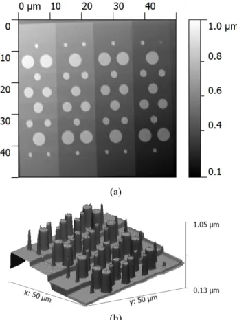
256 pixels at a scan rate of 0.625 line/s. In addition to the topography image (Fig. 2), the NSMM provides both magnitude and phase images of the complex reflection coefficient Γ.
(a)
(b)
Fig. 2. NSMM topography image in (a) 2D view and (b) 3D view.
After data leveling using GwyddionTM software, tilt effects are
corrected. Topography images for the smallest capacitors are given in Fig. 3. Although the capacitors are located on the upper and lower parts of the verification kit (Fig. 1), good agreement in the measured topography is noticed. Furthermore, the thicknesses of the SiO2 are identical at the
different Y-locations.
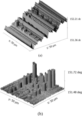
Fig. 3. 1D topography X-scans for the smallest capacitors. The microwave image of the magnitude of the reflection is given in Fig. 4(a). The raw data shows a linear drift only for the Y-direction. This latter is mainly attributed to the VNA measurement configuration that is resynchronized with the topography image line by line. Consequently, a step line correction is applied to resynchronize the data [Fig. 4(b)]. Same findings are obtained for the phase-shift image, i.e. phase-jumps in synchronization can be corrected (Fig. 5). Second step was to verify a possible correlation of the signals fluctuations between topography and microwave data. As illustrated in Fig. 6, the 1D scan regarding the capacitor indicated non-correlated fluctuations between topography and microwave signals. Therefore, fluctuations on the microwave signals are mainly attributed to the source and receiver noises of the VNA. No matching strategy is considered in this study, resulting in relatively poor measurement sensitivity. Indeed, fluctuations in the microwave signals become predominant for the smallest capacitors.
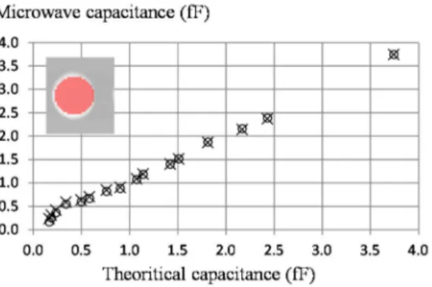
Third step was to apply a vector calibration technique based on a modified SOL technique [11]. To that end, three theoretical capacitance values, obtained from FEM simulation, are considered as capacitances standards to derive the capacitance values at the tip apex of the probe. To lower the measurement uncertainty, the measured capacitance values for each case are obtained as the average capacitance calculated on the whole capacitor surface (see inset of Fig. 7). The calibrated capacitances are given in Fig. 7 as a function of their theoretical counterparts. From these data, we demonstrate that capacitance values down to 500aF can be measured accurately without matching network between the VNA and the probe. To lower the measurement uncertainty, the microwave path should be kept as low less as possible.
(a)
(b)
Fig. 4. 3D Image of the magnitude of the complex reflection coefficient Γ (a) before and (b) after step line correction – F = 9.95GHz.
(a)
(b)
Fig. 5. 3D Image of the phase of the complex reflection coefficient Γ (a) before and (b) after step line correction – F = 9.95GHz.
Fig. 6. 1D scan of a 2µm-wide capacitor. (a) Topography. (b) Magnitude and (c) Phase of the reflection coefficient Γ - F = 9.95GHz.
Fig. 7. Microwave capacitance as a function of the
theoretical values – F = 9.95GHz. Two set of capacitances standards are considered.
IV. CONCLUSION
Atomic force microscopy (AFM) image together with the magnitude and phase-shift images of the complex microwave reflection coefficient using a KeysightTM’s LS5600 AFM interfaced directly with a vector network analyzer, without electrical matching strategy, are performed around 9.5GHz. From a detailed analysis of the raw data, quantitative capacitances extraction indicates a limitation around 500aF. Above 500 aF, noise effects are predominant and must be reduced. Strategies to enhance the measurement accuracy will be discussed in the final version of the paper.
ACKNOWLEDGMENT
This work is performed under EMPIR Planarcal project (http://www.planarcal.ptb.de). This work used the facilities within the EQPX ExCELSiOR (www.excelsior-ncc.eu) funded by the National Research Agency (ANR).
REFERENCES
[1] S. M. Anlage, V. V. Talanov, and A. R. Schwartz, “Principles of near-field microwave microscopy,” Scanning Probe Microscopy: Electrical
and Electromechanical Phenomena at the Nanoscale, S. Kalinin and A. Gruverman, Eds. New York, Springer Sci., pp. 215–253, Aug. 2007.
[2] S. Fabiani, D. Mencarelli, A. Di Donato, T. Monti, G. Venanzoni, A Morini, T. Rozzi, and M. Farina, “Broadband Scanning Microwave Microscopy investigation of graphene”, Proc. IEEE MTT-S
International Microw. Symp., pp. 1-4, June 2011.
[3] G. Gramse, M. Kasper, L. Fumagalli, G. Gomila, P. Hinterdorfer and F. Kienberger, “Calibrated complex impedance and permitivity measurements with SMM,” Nanotechnology, vol. 25, no. 14, p. 8, 2014. [4] Agilent Technologies, Inc., “Scanning Microwave Microscopy (SMM)
Mode”, Datasheet, 2013.
[5] Oxford Instruments, Inc., “Scanning Microwave Impedance Microscopy (sMIM)”, Datasheet, 2014.
[6] A. Imtiaz, T. M. Wallis and P. Kabos, "Near-Field Scanning Microwave Microscopy: An Emerging Research Tool for Nanoscale Metrology”,
IEEE Microwave Magazine, vol.15, no.1, pp.52-64, Jan. 2014.
[7] Olaf C. Haenssler et al, “Integration of a Scanning Microwave Microscope and a Scanning Electron Microscope: Towards a new instrument to imaging, characterizing and manipulating at the nanoscale”, (3M-NANO), 2014 International Conference on. IEEE, 2014. p. 39-43.
[8] Olaf C. Haenssler and S. Fatikow, “Manipulating and characterizing with nanorobotics: In-situ SEM technique for centimeter and millimeter waves”, In : Infrared, Millimeter, and Terahertz waves (IRMMW-THz),
2015 40th International Conference on. IEEE, 2015. p. 1-2.
[9] Zhang, Lan, et al. "Microwave atomic force microscopy imaging for nanometer-scale electrical property characterization." Review of
Scientific Instruments 81.12 (2010): 123708.
[10] K. Haddadi, D. Glay and Tuami Lasri, A 60 GHz scanning near-field microscope with high spatial resolution sub-surface imaging, IEEE
Microw. Wirel. Compon. Lett., 21, no. 11, pp. 625-627, 2011.
[11] T. Dargent, K. Haddadi, T. Lasri, N. Clément, D. Ducatteau, B. Legrand, H. Tanbakuchi, and D. Théron, “An interferometric scanning microwave microscope and calibration method for sub-fF microwave measurements”, Rev. Sci. Instrum., vol. 84, no.12, pp. 123705-123705-7, Dec. 2013.
[12] H. Happy, K. Haddadi, D. Théron, T. Lasri and G. Dambrine, “Measurement techniques for RF nanoelectronic devices : new equipment to overcome the problems of impedance and scale mismatch”,
IEEE Microwave Magazine, vol. 15, no. 1, pp. 30-39.