HAL Id: hal-00707524
https://hal.archives-ouvertes.fr/hal-00707524
Submitted on 12 Jun 2012
HAL is a multi-disciplinary open access
archive for the deposit and dissemination of
sci-entific research documents, whether they are
pub-lished or not. The documents may come from
teaching and research institutions in France or
abroad, or from public or private research centers.
L’archive ouverte pluridisciplinaire HAL, est
destinée au dépôt et à la diffusion de documents
scientifiques de niveau recherche, publiés ou non,
émanant des établissements d’enseignement et de
recherche français ou étrangers, des laboratoires
publics ou privés.
Direct Observation of Massless Domain Wall Dynamics
in Nanostripes with Perpendicular Magnetic Anisotropy
Jan Vogel, Marlio Bonfim, Nicolas Rougemaille, Olivier Boulle, Ioan Mihai
Miron, Stéphane Auffret, Bernard Rodmacq, Gilles Gaudin, J. C. Cezar,
Fausto Sirotti, et al.
To cite this version:
Jan Vogel, Marlio Bonfim, Nicolas Rougemaille, Olivier Boulle, Ioan Mihai Miron, et al..
Di-rect Observation of Massless Domain Wall Dynamics in Nanostripes with Perpendicular
Mag-netic Anisotropy.
Physical Review Letters, American Physical Society, 2012, 108, pp.247202.
�10.1103/PhysRevLett.108.247202�. �hal-00707524�
Perpendicular Magnetic Anisotropy
J. Vogel,1, ∗ M. Bonfim,1, 2 N. Rougemaille,1 O. Boulle,3 I.M. Miron,3 S. Auffret,3
B. Rodmacq,3 G. Gaudin,3 J.C. Cezar,4 F. Sirotti,5 and S. Pizzini1, †
1
Institut N´eel, CNRS and UJF, BP166, 38042 Grenoble, France
2
Departamento de Engenharia El´etrica, Universidade do Paran´a, CEP 81531-990, Curitiba, Brazil
3
SPINTEC, UMR 8191, CEA/CNRS/UJF/Grenoble-INP, INAC, 38054 Grenoble Cedex, France
4
ESRF, BP200, 38043 Grenoble, France
5
Synchrotron SOLEIL, L’Orme des Merisiers, Saint-Aubin, 91192 Gif-sur-Yvette, France Domain wall motion induced by nanosecond current pulses in nanostripes with perpendicular magnetic anisotropy (Pt/Co/AlOx) is shown to exhibit negligible inertia. Time-resolved magnetic
microscopy during current pulses reveals that the domain walls start moving, with a constant speed, as soon as the current reaches a constant amplitude, and no or little motion takes place after the end of the pulse. The very low ‘mass’ of these domain walls is attributed to the combination of their narrow width and high damping parameter α. Such a small inertia should allow accurate control of domain wall motion, by tuning the duration and amplitude of the current pulses.
The interaction between conduction electron spins and local magnetization leads to a wealth of fascinating phe-nomena that have been extensively studied over the last fifteen years. This interaction allows, for instance, ma-nipulating magnetic domain walls in nanostructures us-ing current pulses [1, 2]. The temporal response of do-main walls to the exciting current pulse is a key point for a better understanding of the interactions. It was recently shown that important transient effects can ex-ist for domain walls in in-plane magnetized nanostripes, leading to a delayed domain wall motion with respect to the current pulse [3, 4]. These transient effects, giv-ing rise to domain wall ‘inertia’ or an effective domain wall ‘mass’ [5], are caused by deformations of the do-main wall internal structure when a current or magnetic field is applied [6–8]. Thomas et al. [4] have shown that in the case of vortex domain walls these deformations can lead to a delay of several nanoseconds of the domain wall motion with respect to the current pulse and tran-sient displacements of the order of 1.5 µm. Besides fun-damental interest, such inertial effects potentially limit the use of domain walls in fast logic or memory devices, and transient times give an upper value of the excita-tion frequency. In this sense, domain walls with no in-ertia, i.e. that react instantaneously to an excitation, are highly desirable. Massless domain walls have been predicted theoretically in cylindrical magnetic nanowires with small diameter (below 50 nm) [9]. The cylindri-cal symmetry should allow the magnetization direction inside the domain wall to rotate around the wire axis without changing the demagnetizing energy and without deformation of the domain wall structure. However, fab-rication and experimental studies of such nanowires are difficult. In this paper, we will show that a very good ap-proximation of massless domain walls can be obtained in more conventional magnetic nanostripes with perpendic-ular magnetic anisotropy and Bloch-type domain walls. Using time-resolved magnetic imaging, we show that in
Pt/Co/AlOx nanostripes the domain walls move with
constant velocity, without transient effects at both the beginning and the end of the pulses. We attribute this absence of inertial effects to the combination of a nar-row domain wall width and a high damping parameter α, leading to a large decrease of domain wall deforma-tions with respect to N´eel-type walls in nanostripes with a planar magnetization.
Current-induced domain wall motion (CIDM) has been studied by magnetic microscopy and electrical measure-ments [10–16], which have allowed determining the po-sition and the internal structure of domain walls before and after the application of current pulses. Direct, micro-scopic observations of domain wall motion during current pulses have been largely elusive until now. These obser-vations are, however, essential for an unambiguous deter-mination of inertial effects in domain wall motion. In this paper, we use time-resolved photoemission electron mi-croscopy combined with x-ray magnetic circular dichro-ism (XMCD-PEEM) [17, 18] to study current-induced motion of domain walls in Pt/Co/AlOxnanostripes with
perpendicular anisotropy. The domain wall position was imaged during the application of 10-100 nanoseconds long current pulses. Our measurements show, in a direct way, that in these nanostripes the transient motion of the do-main walls, which are expected to be of Bloch type in this material, is smaller than about 20 nm both at the beginning and at the end of the pulses, and thus much smaller than the displacements observed for N´eel-type walls [3, 4].
Nanostructures based on asymmetric stacks of Pt/Co/AlOx are promising for new spintronic devices
based on the manipulation of magnetization using cur-rent pulses [19–22]. The Rashba interaction, induced by the structural inversion asymmetry, leads to a high spin-torque efficiency and very high domain wall mobilities in this system [21].
mag-2
netron sputtering on resistive Si, were patterned into twenty parallel 500 nm wide and 10 µm long stripes by e-beam lithography and Ion Beam Etching. Ti/Au electri-cal contacts were fabricated by UV lithography. A Scan-ning Electron Microscopy image of the sample is shown in Fig. 1. XMCD-PEEM measurements were performed at the TEMPO beamline of the SOLEIL synchrotron, us-ing a Focus IS-PEEM. The magnetic contrast in the Co layer was optimized by subtracting two consecutive im-ages collected at the Co L3 absorption edge (778.1 eV)
with 100% left and right circularly polarized x-rays re-spectively. For each circular polarization, 60 images of 0.5 s were averaged, after correcting for possible image drifts. Temporal resolution was obtained by synchroniz-ing the nanosecond current pulses applied to the sam-ple with the x-ray pulses of the synchrotron single-bunch mode, where photon bunches reach the sample at a rep-etition rate of 846 kHz. The temporal evolution of the domain wall position in the nanostripes was obtained by recording images for different delays between the current and photon pulses [17, 23]. If events are reproducible for each current pulse, the temporal resolution of this pump-probe technique is limited only by the duration of the photon pulses (about 50 ps) and the jitter between pump and probe (about 100 ps). The total acquisition time of 1 minute for each XMCD image implies that se-quences of about 5 × 10⁷ current (pump) and photon
(probe) pulses were averaged.
FIG. 1. Scanning Electron Microscopy image showing part of the twenty nanostripes connected in parallel to a pulsed voltage source. The Pt/Co/AlOx pads and lines show up in
light grey, while the silicon substrate is dark grey. The gold contacts for current injection are schematically indicated with the dashed boxes.
In order to obtain a well-defined, reproducible initial domain wall position before each current pulse, the fol-lowing procedure was used : i) starting from a saturated state, a 10 µs field pulse was applied perpendicular to the sample plane to create a domain wall in several nanos-tripes; ii) using a sequence of current pulses, the do-main walls were driven to the top exit of the nanostripes, where the increasing cross section inhibits further motion in the up direction; iii) bipolar current pulses with the same positive and negative amplitudes but a longer pos-itive pulse were then applied for the stroboscopic
mea-surements. The domain wall motion was studied during the negative part of the bipolar pulses, which drive the domain walls into the stripes, while the longer positive part of the pulses was used to reset the domain walls to their initial position. The measurements were car-ried out for several time delays, before, during and af-ter the negative driving pulse, with time steps of 5-20 ns. Measurements were performed for current densities J1 = 7.7 × 10¹¹ A/m2 and J2 = 1.3 × 10¹²A/m2. The
driving (reset) current pulse was 120 ns (160 ns) for J1
and 30 ns (40 ns) for J2. The risetime was of the order
of 4 ns for all pulses.
In a PEEM microscope, the image of the sample is formed using the photoelectrons extracted from the sam-ple surface. In order to obtain a sharp image, the poten-tial between the focussing lens and the sample has to be adjusted accurately. Since the sample potential is mod-ified during the current (voltage) pulses, upon scanning the delay between photon and current pulses it can be easily detected when they arrive on the sample at the same time, with an accuracy of about 100 ps. During the current pulses a potential drop is present between the extremities of the stripes (about 3 V for the images of Fig. 2). This implies that the image cannot be well-focussed over the whole length of the stripes. This po-tential drop, and thus the image deformation, increases with increasing current density.
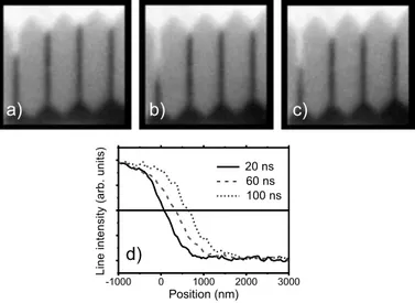
FIG. 2. Time-resolved XMCD-PEEM images taken during current pulses with a current density of 7.7 × 10¹¹
A/m2
, for delays of 20 ns (a), 60 ns (b) and 100 ns (c) after the beginning of the pulse. Line scans of the XMCD intensity averaged over the three stripes on the right are given in (d). The zero position in this graph corresponds to the initial position of the domain walls at the top entrance of the stripes.
Figure 2 shows XMCD-PEEM images for a selection of the twenty nanostripes present in our sample. The three images were taken during current pulses with a current density of J1= 7.7 × 10¹¹A/m
2
ns and 100 ns after the onset of the drive current pulse. The images are corrected for the deformations induced by the voltage drop over the stripe length. In three of the four stripes shown in Fig. 2 the domain wall positions are well-defined for each delay, and the domain walls move reproducibly from up to down [24] in the direction oppo-site to the electron flow [25]. The behavior of the domain wall in the left stripe is much more stochastic, probably due to some strong pinning sites in the middle of the stripe, where the DW sometimes stays blocked for a cer-tain time. This anomalous behavior was observed only in this stripe, while the dynamical behavior of the other lines was very similar, allowing data averaging to improve data quality.
The domain wall position for each time delay was ob-tained from the linescans of the XMCD intensity along each nanostripe. The domain wall displacement was de-fined with respect to the domain wall position before the driving pulse, corresponding to the top entrance of the stripes. The line scans averaged over the three rightmost stripes in Fig. 2(a)-(c) are given in Fig. 2(d). The cor-responding domain wall displacements for all measured delays, with time steps of 5-10 ns, are given in Fig. 3. The driving current pulse is shown in the same figure. The first important information provided by the time-resolved measurements is that the averaged domain wall displacement during the current pulse is linear in time, i.e. the DWs move at a constant average velocity. The velocity, obtained from a linear fit to the data, is 7 ± 1 m/s. Inertial effects should show up as a ‘delay’ of the beginning of the constant velocity regime with respect to the beginning of the pulse [4]. The fit crosses y = 0 at 4.4 ± 2.9 ns from the beginning of the pulse. If we con-sider that the motion during the 4 ns risetime of the pulse is negligible, the motion starts thus within 0.4 ± 2.9 ns from the onset of the ‘plateau’ of constant current den-sity. The maximum time delay (including the error bar) of about 3 ns corresponds to a maximum displacement delay of 3 ns × 7 m/s = 21 nm [26].
We also measured the DW displacements for a 30 ns driving pulse with current density J2= 1.3 × 10¹²A/m2.
Due to the higher voltage drop on the sample, the de-formation of the images used to obtain these data was larger, leading to larger error bars. The average DW velocity obtained from the linear fit of the data points taken during the pulse is 45 ± 10 m/s, with a delay with respect to the beginning of the current pulse of 0.8±5 ns. Transient effects are therefore small also for this higher current density.
In our previous work [21], we have shown that for cur-rent densities smaller than 2 × 10¹² A/m2
the domain wall motion in Pt/Co/AlOxnanostripes is influenced by
thermally activated depinning and can be described by the so-called creep law. Note that this thermally assisted depinning does not influence the domain wall speed av-eraged over a large number of displacements, but it leads
FIG. 3. (color online) The domain wall displacements, aver-aged over the three stripes on the right of the images in Fig. 2, as a function of time (black squares, left axis). The driving pulse with a current density of 7.7 × 10¹¹
A/m2
is also shown (continuous line, right axis). The dashed line is a linear fit to the data points taken during the current pulse. The slope gives a domain wall velocity of 7 ± 1 m/s. The error bars are determined by the spread in displacement values for the three stripes, the error bar on the time is less than the width of the points.
to a distribution of domain wall positions that becomes wider when the average displacement is larger [19]. This is reflected in the increase of the error bar as a function of time in Fig. 3. The domain velocities of 7 ± 1 m/s for J1 and 45 ± 10 m/s for J2obtained here are in good
agreement with the ones we obtained on similar samples with Kerr microscopy [19, 21], where the average domain wall velocities were extracted from the slope of the dis-placement versus pulse duration.
Our data directly show that the transient motion of the domain walls is very small both at the onset and at the end of the current pulses, corresponding to a very small effective domain wall mass. According to Thiaville et al. [8], the domain wall internal structure is modified under the action of a field or current pulse, and the transient displacement depends on the change of generalized angle, δφ : δq = −∆
α(1 − β
α)δφ. In this formula, δq is the change
in domain wall position, ∆ the domain wall width at rest, α the damping parameter and β the non-adiabatic parameter [7, 27]. For a Bloch wall in a nanostripe, φ corresponds to the tilt angle of the magnetization in the center of the wall with respect to the wall plane, in the direction parallel to the nanostripe. Above an angle φ of 45◦, the DW transforms into a N´eel wall, then in a
Bloch wall with opposite chirality (the so-called Walker limit). For the current densities used here, we have shown previously that the domain wall motion in our samples should be in the regime below the Walker breakdown [21], and the maximum value φ can take during domain wall propagation is thus 45◦.
One situation possibly leading to negligible transient effects (δq ≈ 0) is when β ≈ α. However, previous exper-iments have shown that βα ≈ 2 in our samples [28], with
4
α ≈ 0.5 and β ≈ 1, leading to (1 −αβ) ≈ −1. The
max-imum transient displacement, for φ = 45◦, would thus
be 0.25π
α × 5 nm ≈ 8 nm, where 5 nm is the
approxi-mate DW width ∆ [21]. This is in good agreement with our experiments. Since the transient motion is propor-tional to ∆, it is expected to be smaller in systems with perpendicular anisotropy with Bloch-type domain walls, which are in general a factor ten to hundred narrower than N´eel-type domain walls in in-plane systems. How-ever, the small transient motion in our system is favored also by the relatively large value of α : for a damping parameter α = 0.02 (typical for permalloy) and βα = 2, the maximum transient motion would be about 200 nm, much larger than our experimental observation. Finally, the angle φ and thus the transient motion should be re-duced by the s-d mediated Rashba field [21].
In conclusion, we have used time-resolved magnetic imaging to directly reveal the absence of transient ef-fects during current-induced domain wall motion in Pt/Co/AlOx nanostripes with perpendicular anisotropy.
We attribute the negligible domain wall mass to the com-bination of a narrow domain wall width, a large value of the damping parameter α and the s-d mediated Rashba field transverse to the nanostripes. Added to the large domain wall velocities obtained in these systems [21] and the good reproducibility of the domain wall displace-ments, such a small domain wall inertia should allow a fast and accurate control of domain wall motion at high repetition rate, by tuning the duration, frequency and amplitude of the current pulses. Our measurements also show the extreme robustness of these Pt/Co/AlOx
nanostripes, since many billions of pulses with current densities higher than 1 × 10¹²A/m2
could be applied at high frequencies without changing their physical proper-ties.
We acknowledge the invaluable technical and exper-imental help of E. Wagner, D. Lepoittevin, L. Delrey, Z. Ishaque and A. Hrabec, as well as O. Fruchart for dis-cussions. Nanofabrication was performed at the Institut N´eel/CNRS ‘Nanofab’ facility in Grenoble. This work was partially supported by the Agence National de la Recherche through projects ANR-07-NANO-034 ‘Voice’ and ANR-11-BS10-008 ‘Esperado’, and by the Fondation Nanosciences.
∗ jan.vogel@grenoble.cnrs.fr † stefania.pizzini@grenoble.cnrs.fr
[1] L. Thomas and S.S.P. Parkin in Handbook of Magnetism and Advanced Magnetic Materials, John Wiley & Sons, Ltd. (2008).
[2] O. Boulle, G. Malinowski, and M. Kl¨aui, Mater. Sci. Eng. R-Rep. 72, 159 (2011).
[3] J.-Y. Chauleau, R. Weil, A. Thiaville, and J. Miltat, Phys. Rev. B 82, 214414 (2010).
[4] L. Thomas, R. Moriya, C. Rettner, and S.S.P. Parkin, Science 330, 1810 (2010).
[5] E. Saitoh, H. Miyajima, T. Yamaoka, and G. Tatara, Nature 432, 203 (2004).
[6] Z. Li and S. Zhang, Phys. Rev. B 69, 134416 (2004). [7] A. Thiaville, Y. Nakatani, J. Miltat, and Y. Suzuki,
Eu-rophys. Lett. 69, 990 (2005).
[8] A. Thiaville, Y. Nakatani, F. Pi´echon, J. Miltat, and T. Ono, Eur. Phys. J. B 60, 15, (2007).
[9] M. Yan, A. K´akay, S. Gliga, and R. Hertel, Phys. Rev. Lett. 104, 057201, (2010).
[10] A. Yamaguchi, T. Ono, S. Nasu, K. Miyake, K. Mibu, and T. Shinjo, Phys. Rev. Lett. 92, 077205 (2004). [11] M. Kl¨aui, P.O. Jubert, R. Allenspach, A. Bischof,
J.A.C. Bland, G. Faini, U. R¨udiger, C.A.F. Vaz, L. Vila, and C. Vouille, Phys. Rev. Lett. 95, 026601 (2005). [12] J.-P. Adam, N. Vernier, J. Ferr´e, A. Thiaville, V. Jeudy,
A. Lemaˆıtre, L. Thevenard, and G. Faini, Phys. Rev. B 80, 193204 (2009).
[13] S. Pizzini, V. Uhl´ıˇr, J. Vogel, N. Rougemaille, S. Laribi, V. Cros, E. Jim´enez, J. Camarero, C. Tieg, E. Bonet, M. Bonfim, R. Mattana, C. Deranlot, F. Petroff, C. Ulysse, G. Faini, and A. Fert, Appl. Phys. Express 2, 023003 (2009).
[14] V. Uhl´ıˇr, S. Pizzini, N. Rougemaille, J. Novotn´y, V. Cros, E. Jim´enez, G. Faini, L. Heyne, F. Sirotti, C. Tieg, A. Bendounan, F. Maccherozzi, R. Belkhou, J. Grollier, A. Anane, and J. Vogel, Phys. Rev. B 81, 224418 (2010). [15] M. Hayashi, L. Thomas, Y. B.Bazaliy, C. Rettner, R. Moriya, X. Jiang, and S. S. P. Parkin, Phys. Rev. Lett. 96, 197207 (2006).
[16] H. Tanigawa, T. Koyama, G. Yamada, D. Chiba, S. Ka-sai, S. Fukami, T. Suzuki,N. Ohshima, N. Ishiwata, Y. Nakatani, and T. Ono, Appl. Phys. Express 2, 053002 (2009).
[17] J. Vogel, W. Kuch, M. Bonfim, J. Camarero, Y. Pen-nec, F.Offi, K.Fukumoto, J. Kirschner, A. Fontaine, and S. Pizzini, Appl. Phys. Lett. 82, 2299 (2003).
[18] G. Sch¨onhense, H. J. Elmers, S. A. Nepijko, and C. M. Schneider, in Advances in Imaging and Electron Physics 142, Elsevier Academic Press Inc., San Diego, USA, 159 (2006).
[19] T. A. Moore, I. M. Miron, G. Gaudin, G. Serret, S. Auf-fret, B. Rodmacq, A. Schuhl, S. Pizzini, J. Vogel, and M. Bonfim, Appl. Phys. Lett. 93, 262504 (2008). [20] I. M. Miron, G. Gaudin, S. Auffret, B. Rodmacq,
A. Schuhl, S. Pizzini, J. Vogel, and P. Gambardella, Na-ture Mater. 9, 230 (2010).
[21] I. M. Miron, T. A. Moore, H. Szambolics, L. Buda-Prejbeanu, S. Auffret, B. Rodmacq, S. Pizzini, J. Vogel, M. Bonfim, A. Schuhl, and G. Gaudin, Nature Mater. 10, 419 (2011).
[22] I. M. Miron, K. Garello, G. Gaudin, P.-J. Zermatten, M. Costache, S. Auffret, S. Bandiera, B. Rodmacq, A. Schuhl, and P. Gambardella, Nature 476, 189 (2011). [23] V. Uhl´ıˇr, S. Pizzini, N. Rougemaille, V. Cros, E. Jim´enez, L. Ranno, O. Fruchart, M. Urb´anek, G. Gaudin, J. Ca-marero, C. Tieg, F. Sirotti, E. Wagner, and J. Vogel, Phys. Rev. B 83, 020406 (2011).
[24] See supplemental material at
http://prl.aps.org/supplemental/PRL/v108/i24/e247202,
or the web pages of the Institut N´eel
(http://neel.cnrs.fr/spip.php?article3238), for a movie of the image series.
[25] T. A. Moore, I. M. Miron, G. Gaudin, G. Serret, S. Auf-fret, B. Rodmacq, A. Schuhl, S. Pizzini, J. Vogel, and M. Bonfim, Appl. Phys. Lett. 95, 179902 (2009). [26] Note that the current direction of our driving pulse is
opposite to the one in the reset pulse, meaning that the current direction reversed at the beginning of eah driv-ing pulse. In Ref. [21] it was shown that a reversal of the current direction is associated to a change of chi-rality of the Bloch domain wall, since the s-d mediated Rashba field switches direction. For a current density of
1.4 × 10¹²
A/m2
, a delay in motion of 20 nm was ob-served, corresponding to a delay time of 0.2 ns at the corresponding DW velocity of 100 m/s. This delay time is well within the error bar of about 3 ns in the present experiment.
[27] S. Zhang and Z. Li, Phys. Rev. Lett. 93, 127204 (2004). [28] I. M. Miron, P.-J. Zermatten, G. Gaudin, S. Auffret, B. Rodmacq, and A. Schuhl, Phys. Rev. Lett. 102, 137202 (2009).

![[Progress of the two ITAES approaches]](data:image/gif;base64,R0lGODlhAQABAIAAAP///wAAACH5BAEAAAAALAAAAAABAAEAAAICRAEAOw==)